行政院國家科學委員會專題研究計畫 期中進度報告
包覆磁性合金碳奈米結構陣列在奈米解析度垂直記錄媒體
之應用
計畫類別: 整合型計畫 計畫編號: NSC93-2120-M-009-003- 執行期間: 93 年 08 月 01 日至 94 年 07 月 31 日 執行單位: 國立交通大學材料科學與工程學系(所) 計畫主持人: 郭正次 共同主持人: 潘扶民,吳宗信 計畫參與人員: 林兆焄、陳柏林、王威翔、張志忠、林貞君、莊必愷、劉祐君、 鄧伊茹、彭玉容、周欣怡、許國賢、陳德銘、張凱鈞等人 報告類型: 精簡報告 報告附件: 出席國際會議研究心得報告及發表論文 處理方式: 本計畫可公開查詢中 華 民 國 94 年 6 月 1 日
行政院國家科學委員會補助專題研究計畫成果報告
※※※※※※※※※※※※※※※※※※※※※※※※※※
※ ※
※ (計畫名稱) ※
※ ※
※※※※※※※※※※※※※※※※※※※※※※※※※※
計畫類別:□個別型計畫 ■整合型計畫
計畫編號:NSC 93-2120-M-009-003-
執行期間:2004 年 8 月 1 日至 2005 年 7 月 31 日
計畫主持人:郭正次
共同主持人:吳宗信、潘扶民
計畫參與人員:林兆焄、陳柏林、王威翔、張志忠、林貞君、莊必愷、
劉祐君、鄧伊茹、彭玉容、周欣怡、許國賢、陳德銘、張凱鈞等人
本成果報告包括以下應繳交之附件:
□赴國外出差或研習心得報告一份
□赴大陸地區出差或研習心得報告一份
□出席國際學術會議心得報告及發表之論文各一份
□國際合作研究計畫國外研究報告書一份
執行單位:國立交通大學 材料科學與工程學系、機械工程學系
中 華 民 國 94 年 5 月 31 日
行政院國家科學委員會專題研究計畫成果報告
奈米解析度記錄媒體及其他應用之包覆合金碳奈米結構陣列,其製
造、機械/熱性質及製程特徵之研究子計畫一(2/3)-包覆磁性合金碳
奈米結構陣列在奈米解析度垂直記錄媒體之應用
Fabrication and characterizations of the alloy-encapsulated carbon
nanostructures for applications in nano-resolution storage media and
others
計畫編號:NSC 93-2120-M-009-003
執行期限:2004 年 8 月 1 日至 2005 年 7 月 31 日
主持人:郭正次 國立交通大學 材料科學與工程學系
共同主持人:吳宗信 國立交通大學 機械工程學系
共同主持人:潘扶民 國立交通大學 材料科學與工程學系
中文摘要 為了達成將相變化合金鑲埋於開口端 碳奈米管 (carbon nanotubes, CNTs)的頂部 孔洞作為奈米解析度儲存媒體之用,首 先,以氫氣與甲烷為氣源,由電子迴旋共 振化學氣相沉積法,以鈷觸媒輔助成長 CNTs。之後,將剛成長出的 CNTs 在氫電 漿環境中作後處理,可將覆蓋觸媒的碳層 去除,緊接著浸泡在 0.25 M 的硝酸溶液 中,則頂端的觸媒可被移除。擁有碗狀頂 部的開口端 CNTs 接著以濺鍍製程,被覆 蓋一層 200 nm 的 Ge2Sb2Te5相變化合金, 之後再於真空中熱處理 30 分鐘,可將 CNTs 管壁周圍的相變化材料修整去除,以得到 管端鑲埋合金之 CNTs。主要的製程參數包 括觸媒厚度、氫氣與甲烷比例、氫電漿後 處理時間、化學蝕刻時間和熱處理溫度。 各個製程步驟的結構與性質分析是以掃描 電子顯微技術、穿透電子顯微技術、歐傑 電子頻譜技術以及場發射量測法完成。 關鍵詞:碳奈米管、迴旋共振化學氣相沈 積、相變化合金、奈米解析度儲存媒體 AbstractIn order to cap the tip cavities of the open-ended carbon nanotubes (CNTs) with
the phase-change alloy for potential applications as the nano-resolution storage media, the Co-assisted CNTs were first synthesized by electron cyclotron resonance chemical vapor deposition (ECR-CVD) with H2 and CH4 as the gas sources. Then, the as-grown CNTs were post-treated in H-plasma atmosphere to remove the carbon layers covered on catalysts, and subsequently immersed in 0.25 M HNO3 solution to remove the catalysts from the tips. The open-ended CNTs with a bowl-like-shape tips were followed by coating with a phase-change alloy layer of Ge2Sb2Te5 (200 nm in thickness) via sputtering process, and then heat treated in vacuum (10-3 Torr) for 30 minutes to trim the alloy off from the sidewalls of CNTs to obtain the alloy-ended CNTs. The main processing parameters include catalyst thickness, H2/CH4 ratio, time of H-plasma post-treatment, chemical etching time and heat-treating temperature. The structures and properties in each processing step were characterized by scanning electron microscopy (SEM), transmission electron microscopy (TEM), Auger electron spectroscopy (AES) and field emission measurements.
Keywords: Carbon nanotubes; Cyclotron
resolution storage media
1. Introduction
Carbon is a very interesting element found in large quantities on the earth. Several carbonaceous structures such as diamond, amorphous carbon film, fullerene (C60), and carbon nanotubes (CNTs), et al. have been discovered. Since Dr. Ijima discovered CNTs [1], numerous research groups all over the world have investigated their growth mechanisms, structures, morphologies, and applications. CNTs have some unique properties so many applications have been proposed, such as electron field emitters [2], structures for storing hydrogen [3], AFM tips [4], and single electron transistors [5], among others. The synthesis of open-ended CNTs has recently been examined because they have properties that differ remarkably from those of close-ended CNTs. Evidences reveals that opening the CNTs tips improves field emission performance and hydrogen storage [6]. Hollow, open-ended CNTs can also be filled with various materials, and so can be used in applications such as magnetic recording and nanothermometry [7] and [8]. Therefore, several methods of fabricating open-ended CNTs, and the corresponding mechanisms, have been proposed in recent years, including oxidation [9], plasma etching [10], electrochemical etching [11] treatment with nitric acid [12] and others. However, most such methods suffer from poor reproducibility and serious structural damage to the CNTs. This work proposes a process for yielding well-aligned open-ended CNTs with a large area, using ECR-CVD combined with post-treatment processes, such H-plasma etching and chemical etching.
So far the phase-change alloys have been commercially used for optical storage applications in rewritable digital versatile disks (DVD). Users require high data storage density. However, its storage capacity is so limited (< 35 Gbyte/in2). In order to increase the storage capacity, the alloy-ended carbon nanostructures were successfully developed to fabricate the nano-resolution phase-change type storage media by coating proper
constituents of phase-change alloys on tips of open-ended CNTs.
2. Experimental
The Co catalyst with a thickness of 10 nm was first deposited on round silicon wafers with a diameter of 4 in. by sputtering process and subsequent pretreatment by a H-plasma in ECR-CVD system. The pretreatment conditions were: microwave power, 800 W; magnetic field, 875 G; H2 flow rate, 15 sccm; substrate temperature, 630 °C; substrate bias, - 150 V; chamber pressure, 10- 3 Torr, and treatment time, 15 min. The well-aligned and close-ended CNTs with large areas were then synthesized using Co-assisted ECR-CVD with a mixture of methane and hydrogen as source gases. The conditions of deposition of the CNTs were: H2/CH4 , 10/20 sccm/sccm; pressure, 10- 3 Torr; substrate temperature, 655 °C; bias, - 150 V, and deposition time, 15 min.
H-plasma post-treatment was used to remove carbon layers from the catalyst of the as-grown CNTs tips to fabricate open-ended CNTs. The etching temperature was varied by changing the treatment time of the H-plasma. The other parameters of H-plasma post-treatment were bias, - 200 V; magnetic field, 875 G; pressure, 10- 3 Torr; microwave power, 575 W, and H2 flow rate, 10 sccm. The H-plasma-post-treated CNTs then underwent chemical etching post- treatment by immersion in nitric acid solution (HNO3:0.25 M) for 3 min. They were then rinsed in deionized water for approximately 1 min, and then dried out on a hot plate at 150 °C for 5 min. Post-treatments were performed under six different conditions (Con1 6), as presented in Table 1. The specimens were subsequently coated with a Ge2Sb2Te5 layer of 200 nm in thickness, and then followed by heat-treatment for 30 min (400℃, 420℃, 440℃).
3. Results and Discussion
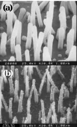
In the first processing step, well-aligned CNTs were fabricated over a large area on a
silicon wafer by ECR-CVD, and the SEM morphology of the as-grown CNTs was as presented in Fig. 1. Fig. 2 and Fig. 3 present the corresponding TEM and HRTEM images, respectively. The close-ended, tubular and Co-encapsulated CNTs had a diameter of 120 nm. The graphite layers in the axial direction presented in Fig. 3 reveal that the CNTs do not comprise nanofibers. The H2/CH4 ratio and substrate bias dominate the morphology of the carbon nanostructures. An excess concentration of carbon in the gas phase may generate rattan-like CNTs surrounded by carbon sheets. The TEM image in Fig. 2 reveals that the tip catalyst particles of the highly aligned tubes were covered with ultra-thin carbon layers that were approximately 3 5 nm thick. Experimental data herein show that the as-grown CNTs cannot easily be etched chemically to remove the catalysts from the tips, because they are protected by the carbon layer on the catalyst surface. This fact was shown experimentally by chemically etching the as-grown CNTs in 0.25 M HNO3 acid solution for 30 min without performing H-plasma etching post- treatment beforehand. The findings reveal that the catalysts could not be removed from the CNTs, which were partly detached from the substrate. Accordingly, H-plasma post- treatment under appropriate conditions can be conducted to remove the carbon layers but without damaging the stems of the CNTs.
Figs. 4(a)–(d) present the SEM images following H-plasma etching post-treatments after etching times of 1, 4, 7 and 10 min, respectively (Con2, Con4, Con5 and Con6), indicating that increasing etching time slowly reduces the number density of the tube and increases the number of destroyed CNTs. The structures of the stems of CNTs are severely damaged after etching for 10 min, as shown in Fig. 4(d). Restated, a particular etching time of, for example 1 min must be used, is required to enable the carbon layers to be removed from the catalyst surface, while maintaining the structural integrity of the CNTs, as presented in Fig. 4(a), with a corresponding TEM image in Fig. 5. The effect of etching can be altered by varying the parameters, such as the microwave power,
the applied bias, the etching time of H-plasma, and the H2 flow rate. Chemical etching can then be used to remove further the carbon layer-stripped CNTs with exposed catalysts.
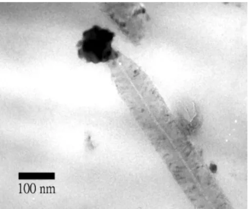
The carbon layer-stripped CNTs were further immersed in 0.25 M HNO3 for 3 min to remove the catalysts from the tips. Fig. 6 and Fig. 7 present the corresponding SEM and TEM images after chemical etching, respectively. The figures demonstrate that the catalysts at the tips can be completely removed, yielding open-ended CNTs. In conclusion, two-step post-treatment that comprises a 1 min H-plasma process and 3 min 0.25 M HNO3 chemical etching was optimal in this case for fabricating open-ended CNTs with high structural integrity and reproducibility.
An attempt was made to remove the catalysts directly from the tip by immersing them into HNO3 for longer but it was useless because the carbon film strongly resisted acid etching. Therefore, the plasma etching procedure must be conducted to remove the carbon film and enable the catalysts to be etched effectively by the following etching procedure.
Table 2 lists the field emission properties of as-grown CNTs following each processing step. Fig. 8 presents J-E plots for CNTs following post-treatment under various conditions. The results indicate that the open-ended CNTs (Con3 in Table 2, Curve 3 in Fig. 8) may behave better than the as-grown tubular CNTs (Con1 in Table 2, Curve 1 in Fig. 8) because the local aspect ratio is higher around open-ended tips, where their structural integrity is maintained during H-plasma post-treatment. However, the field emission properties of the carbon layer- stripped CNTs (Con2 in Table 2, Curve 2 in Fig. 8) are less favorable than those of as-grown CNTs because the exposed catalysts without carbon layer protection are oxidized. If H-plasma post-treatment, with an etching time of approximately 10 min, (Con6 in Table 2, Curve 4 in Fig. 8), destroys the structural integrity, then the field emission properties will be the worst possible. Well- aligned open-ended CNTs with high
structural integrity are thus determined to have better field emission properties. CNTs have better emission properties at a higher turn-on voltage and a lower field emission current density because the heavy plasma in the ECR-CVD system produces defects.
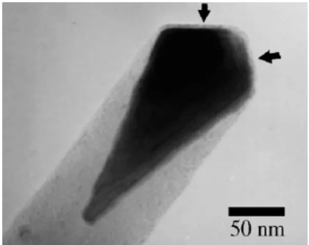
SEM images of open-ended CNTs covered with 200 nm phase-change alloy, and then heated at 420℃ for 30 min are shown in Figs. 9(a) and (b), respectively. Fig. 10 is the corresponding TEM images of Fig. 9(b). It represents the alloy-coated open-ended CNTs can be heat treated to trim off the alloys from their sidewalls in vacuum at 420oC for 30 min to become an alloy-ended CNTs. Furthermore, the Auger analysis of phase- change alloy on CNTs (Fig. 11) shows that the sputtering process must be modified to obtain the required composition of phase- change alloy after being capped on the tips of CNTs, where the compositions of the phase- change alloys may be changed from Te-rich to Ge-rich due to the faster evaporation rates of Sb and Te (Sb and Te have lower melting point and heat of vaporization than Ge).
4. Conclusions
The work presents a flexible and reproducible method for producing well- aligned open-ended CNTs over a large area, with good structural integrity, on a 4-inch Si wafer. The process comprises catalyst- assisted CNTs growth, H-plasma post- treatment and chemical etching. The etching effect is easily optimized to generate open- ended CNTs with good structural integrity. Other advantages of the process are its simplicity, reproducibility and potential application for mass-production. The process has several other adjustable parameters to improve performance, including microwave power, applied bias, etching time with H-plasma, H2 flow rate and others. The results indicate that the as-grown CNTs can be further processed to alter their tip configuration to improve their field emission properties. The tip configuration includes the numerical density of the tubes, the aspect ratio of the tips. The purpose of capping open-ended CNTs tips with phase-change
alloy can be carried out by alloy sputtering process and followed by proper heating.
References
[1] S. Iijima, Nature 354 (1991), p. 56.
[2] A.G. Rinzler, J.H. Hafber, P. Nikolaev, L. Lou,
S.G. Kim, D. Tomanek, P. Norlander, D.T. Colbert and R.E. Smalley, Science 269 (1995), p. 1550.
[3] C. Liu, Y.Y. Fan, M. Liu, H.T. Cong, H.M.
Cheng and M.S. Dresselhaus, Science 286 (1999), p. 1127.
[4] H.J. Dai, J.H. Halfner, A.G. Rinzler, D.T.
Colbert and R.E. Smalley, Nature 384 (1996), p. 147.
[5] Y.T. Tan, T. Kamiya, Z.A.K. Durrani and H.
Ahmed, J. Appl. Phys. 94 (2003), p. 633.
[6] H. Lee, Y.S. Kang, S.H. Kim and J.Y. Lee, Appl.
Phys. Lett. 80 (2002), p. 577.
[7] J. Bao, Q. Zhou, J. Hong and Z. Xu, Appl. Phys.
Lett 81 (2002), p. 4592.
[8] Y. Gao, Y. Bando and D. Golberg, Appl. Phys.
Lett. 81 (2002), p. 4133.
[9] S.H. Tsai, C.W. Chao, C.L. Lee and H.C. Shiha,
Appl. Phys. Lett. 74 (1999), p. 3462.
[10] S.J. Chung, S.H. Lim and J. Jang, Thin Solid
Films 383 (2001), p. 73.
[11] N. Wang and B.D. Yao, Appl. Phys. Lett. 78 (2001), p. 4028.
[12] S.C. Tsang, Y.K. Chen, P.J.F. Harris and M.L.H. Green, Nature 372 (1994), p. 159.
Table 1: Conditions for H-plasma and chemical etching post-treatments of as-grown CNTs.
Table 2: Field emission properties of as-grown CNTs following various post-treatments
Fig.1: Typical SEM micrograph of typical as-grown CNTs.
Fig. 2: TEM micrograph of as-grown CNTs with carbon layers on the catalyst.
Fig. 3: HRTEM micrograph of the tip of as-grown CNTs showing graphite layers in the direction of growth.
Fig. 4: Typical SEM micrographs of the as-grown CNTs following H-plasma post-treatment for various durations: (a) 1, (b) 4, (c) 7 and (d) 10 min.
Fig. 5: TEM micrograph of as-grown Co-assisted CNTs following H-plasma post-treatment, showing removal of carbon layers on the catalyst surface (Con2).
Fig. 6: SEM morphology of as-grown CNTs following post-treatment (Con3) showing the open-ends.
Fig. 7: TEM micrograph, corresponding to Fig. 6.
Fig. 8: J-E curves of the as-grown CNTs after post-treatment under various conditions. Curves 1 to 4 correspond to Con1 to Con3 and Con6, respectively.
Fig. 9: SEM images of open-ended CNTs covered with 200 nm phase-change alloy (a), and then heated at 420℃ for 30 min (b).
(a)
Fig. 10: the corresponding TEM images of Fig. 9(b). 0 200 400 600 800 1000 1200 4200C for 30 min Si C Sn O Ge dN/dE Electron Energy(eV)
Fig. 11: Auger analysis of phase-change alloy on CNTs.
行政院國家科學委員會專題研究計畫成果報告
奈米解析度記錄媒體及其他應用之包覆合金碳奈米結構陣列,其
製造、機械/熱性質及製程特徵之研究子計畫三(2/3)-電子迴旋
共振化學汽相沉積反應腔體中電漿製程模擬 (Plasma flow
simulation for nanostructure formation in ECR-CVD chamber)
計畫編號:NSC 93-2120-M-009-002
執行期限:2004 年 8 月 1 日至 2005 年 7 月 31 日
主持人:吳宗信 國立交通大學機械工程學系
中文摘要 在本研究計劃,吾人將以數值方法, 模擬用來製造奈米碳管等相關製程的電子 迴旋共振化學氣相沈積電漿源腔體,內部 中甲烷/氫氣混合氣體電漿流場。在第二年 中,延續第一年建制之軟、硬體,吾人已 成功建立電漿流場模擬中,諸多重要的原 始程式碼也已陸續開發完成測試,如下列 所示:平行帶電粒子與中性原子間蒙地卡 羅碰撞法,和三維馬克思威爾方程程式 碼 , 將 在 本 報 告 中 說 明 。 另 外 , 整 合 Poisson’s equation 及 PIC/MCC 之平行程式 也將以 DC- 及 RF-discharge 電漿來驗証其 正確性。最後,未來一年的工作規畫也將 提出報告。 關鍵詞:奈米碳管、迴旋共振化學氣相沈 積、Poisson 方程式、向量 Poisson 方程式、 馬克思威爾方程程式、PIC/MCC。 AbstractIn this project, we intend to simulate the plasma flow using methane/hydrogen gases as the precursors in an ECR-CVD (electron cyclotron resonance) chamber, which is used to manufacture nanotube-like structure in other related projects. In the second year, following the tasks in the first year, we have successfully completed the coding and test of several important portions of the simulation tool. These include the particle-in-cell (PIC) coupled with Monte Carlo collision (MCC), which considers the collision of charged particle with the background neutral gas, and the 3-D Maxwell equation solver using
edge-based finite element method. Completed parallel PIC/MCC is verified by two cases including quasi-1D DC-discharge and RF-discharge of argon gas. At the end, the tasks in the third year are outlined and discussed.
Keywords: plasma flow, edge-based finite
element, Poisson equation, Maxwell’s equation, particle in cell, Monte Carlo collision.
1. INTRODUCTION
In the other related project [1], ECR-CVD chamber has been used to manufacture nanostructures that can be potentially applied in higher-area-density magnetic recording media. The success of the materials processing forming nanostructures in this direction more or less depends upon trials-and-errors method. No systematic theoretical or modeling study has been conducted. To optimize the materials processing in forming nanostructures, fundamental understanding of the plasma flow inside the ECR-CVD chamber is inevitable, although it is very complicated in essence. In this project, we have aimed at simulating the complicated plasma flow features inside the ECR-CVD chamber within 3-year project.
Materials processing plasmas have been modeled numerically using either the fluid model [2] or the particle model [3]. The fluid model is computationally much more efficient if mobility and diffusion coefficients are provided in advance. The fluid model is
valid when the electron density distribution is close to the Maxwellian. If the deviation cannot be neglected, the particle method has to be used for simulating the plasma. The particle method is a solution method for solving the Boltzmann equation. The particle method is a realization of this stochastic process using uniform random numbers (Monte Carlo simulation).
Advantages of the particle method include the justified application to low-pressure plasma as in the ECR-CVD chamber, energy distribution functions of electrons and ions as part of the solution, and unnecessary evaluation of mobilities, diffusion coefficients, and relaxation times for various values of reduced electric field, driving frequency and magnetic field.
The study was planned to be able to model the full-scale methane/hydrogen plasma flow inside the ECR-CVD chamber at the end of the three-year project. In this report, we describe briefly the preliminary results developed in the second year and also the future tasks in the third year.
2. NUMERICAL METHOD
In this section, we will describe respectively the numerical methods employed for solving related governing equations. In the first-year report, we have described the progress and details of the numerical method for the Poisson’s equation for electrostatics, vector Poisson’s equation for magnetostatics and collisionless PIC method. Also in the first-year report, parallel processing on unstructured mesh using graph-partitioning technique has been presented. In this second-year report, we will only describe the details of the PIC with Monte Carlo collisions and 3D Maxwell’s equation solver using edge-based finite element method.
2.1 PIC/MCC method
The PIC method [4] was originally designed for collisionless charged particle simulations. It models the movement of charged particles under the influence of Lorentz force (F =q(E+v×B), q: particle charge, E: electric field, B: magnetic field) and solves the field equations (Maxwell or
Poisson equation) due to redistribution of charge density (ρ) and charge current (J) at each time step. A mesh is introduced to sample the space charge and current distributions that enter the field equation. The sampling is performed by appropriate charge
assignment from the particle locations to the
grid points. Afterwards, the computed fields (E & B) from field equations at grid points are interpolated back to the charge-particle positions. Then, charged particles are moved to their new positions using the concept of
Boris rotation [3] without actually computing
the forces explicitly. This process repeats itself to obtain the self-consistent solution during the simulation. This is the so-called particle-in-cell (PIC) method.
In order to reproduce plasmas, one has to inevitably resolve the smallest time scale, i.e., electron time scale. It is estimated that electrons are the fastest particle in the plasma, with their velocities in the range of 105-106 m/s. Thus, this requires an electron time step of 10-10-10-9 s to properly model the electron trajectories in the presence of magnetic field. Thus, the time steps of ion and electron would be very much different to obtain the correct physics.
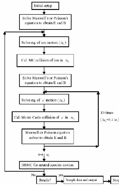
In addition, the so-called PIC/MCC method is to include the MC collisions, in the PIC method, between charged particles, and neutral particles and charged particles under the circumstances of weakly ionized plasma. This concept can be clearly shown in Fig. 1. The collisions between charged particles (or Coulomb collisions) are often neglected if low plasma density is concerned, as is the case in the bulk plasma region in DC-magnetron sputtering chamber. Only the collisions between charged particle and neutral particle will be taken into account in the current proposed study. In dealing with these collisions using Monte Carlo method, reliable cross section data are required.
2.2 3-D Maxwell
equation solver
2.45GHz microwave is used to deposit power from the top into the plasma. Thus, solution of 3D Maxwell’s equation at each simulation time step is required to self-consistently solve the instantaneous EM field due to the motion of charged particles and imposed microwave field. One of the most important and challenging tasks in the second year is to develop a 3D Maxwell equation solver using edge-based finite element method. Related developments are reported in the following.
Original Maxwell’s equations are presented in the following form.
where D =εE, B =µH , J =σE in which
e, µ and s is the permittivity, permeability &
conductivity of the medium, respectively. They are then combined into the following form as, by eliminating H ,
and related BC conditions as n×E(r,t)=0 for perfect conductor. Once the electric field is obtained from the above wave equation, magnetic field can then be derived from the Farady’s law directly.
In the current study, we have used edge-based Galerkin finite element method for discretizing the electric-field wave equation in spatial coordinates. Expanding the electric field as
) ( ) ( ) , ( 1 r N r E j N j j t u t
∑
= =whern Nj(r) is the vector shape function. In the current study, linear shape function is used throughout the current study. We then can obtain the matrix equation written as
[ ]
{ }2 ([ ] [ ]) { } [ ]{ } { } {0} 2 = + + + + S u f dt u d Q R dt u d T where [ ] [ ][
]
∫∫
∫∫∫
∫∫∫
∫∫
∫∫∫
∫∫∫
⋅ ⋅ ⋅ ⋅ ⋅ ⋅ + ∂ ∂ = × ∇ × ∇ = × × = = = S i i i i V i j ij S i j ij j V i ij j V i ij dS t dV t t f dV S dS n n Y Q dV R dV T ) , ( ) ( ) , ( ) ( ) ( ) ( 1 )] ( ˆ [ ) ( ˆ ) ( ) ( ) ( ) ( r U r N r J r N r N r N r N r N r N r N r N r N V µ σ εNow Newmark-β method with γ=1/2 and
β=0.25 is employed for discretizing temporal direction. Resulting algebraic matrix equation is rearranged as
The above matrix equation is then solved using complex conjugate gradient method [5] at each time step.
3. RESULTS AND DISCUSSIONS 3.1 Parallel coupled PIC/MCC solver
Completed parallel PIC/MCC code is verified by computing two examples: 1D gas discharge with direct current (DC) source and radio frequency (RF) source. Both voltage sources are used throughout the study. However, only the case of RF voltage source is shown for clarity. Corresponding results and discussions are presented in the following.
RF discharge
Argon gas with 50 mtorr is used as the background gas having a RF voltage source with amplitude of 500 volts and frequency of 13.56 MHz applied at the cathode, while the anode is grounded. Distance between parallel plates is 20 mm without considering the
(Faraday's law) (Ampere's law) ? (Gauss's law) 0 (Gauss's law-magnetic) ? (equa B E t D H J t B J t
D
∂ ∇× = − ∂ ∂ ∇× = + ∂ ∇ = ∇ = ∂ ∇ = − ∂⋅
⋅
⋅
tion of continuity) 2 2 ( , ) 1 ( , ) ( , ) ( , ) i t t t t e s µ t t t ∂ ∂ ∂ ∇× ∇× + + = − ∂ ∂ ∂ J r E r E r E r { } { } { } 1 2 2 1 2 1 2 (1 2 ) 1 [ ] [ ] [ ] [ ] [ ] ( 2 )[ ] 2 ( ) ( ) 1 1 1 [ ] [ ] ( )[ ] 2 ( ) n n s s n s ? ? T T ß S n T T ? ß S n t t t t ? T T ? ß S n t t + − + + = − − − + − ∆ ∆ ∆ ∆ − −∆ − ∆ + − + 1 1 1 1 { } ( 2 ){ } ( ){ } 2 2 [ ] [ ] [ ] n n n s ß f ? ß f ? ß f where T R Q + − − + + − + − + = +secondary electron emission since the major mechanism for maintaining the plasma is due to the oscillation of the RF field. In addition, directions transverse to the direction of the gap are all set to be Neumann condition since our code is three-dimensional in essence.
In the simulation ∆t=5×10⁻¹¹sec, 400 cells in the gap direction. Total number of elements is about 14,000 (~2800 nodes). Data presented below are averaged from the sample after running for at least 200 RF cycles, which should safely remove transient effects. Total number of particles is in the range of 0.4-0.5 millions, with approximately 20 particles for ions and electrons. 2000 time steps are used to resolve one period of the RF source.
Figs. 2a-2f show the simulation results with the test and simulation conditions as described in the above. Fig. 2a illustrates the four instantaneous distributions (t=0, 1/4T, 1/2T, T) of potential distribution, while Fig. 2b presents the corresponding distributions of electrical field. Since this is a symmetric RF gas discharge, no DC bias at the cathode can be found. Averaged plasma potential in the bulk is about 250 volts, while the electrical field in the bulk is nearly zero at all times during a complete RF cycle. Sheath thickness is about 3 mm on each electrode.
Fig. 2c shows the corresponding averaged distribution of number density for argon ion and electron. Ion and electron number densities are nearly the same in the plasma bulk region with the highest value of 1.5E16 m-3, while the ion number density is higher than electron number density in the sheath, which makes the sheath positively charged on the average. Fig. 2d illustrates the corresponding distribution of averaged ion and electron energy. Electron energy is slightly less than 3 eV in the bulk, while it begins at 5 mm from the electrode to decrease to zero at the electrode. The ion energy can be as high as 20 eV near the electrode, while it is nearly zero in the plasma bulk since its mass is too large to respond to the oscillation of the RF source. This large ion energy near the electrode plays an important role in plasma materials processing.
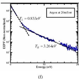
Fig. 2e shows the non-normalized electron energy probability function (EEPF) at argon pressure of 50 mttor, which is considered to be high in the current study. Slightly bi-Maxwellian distribution can be found by fitting the electron temperature at low- and high-energy range. Resulting low and high electron temperatures are 1.58 eV and 2.58 eV, respectively. In addition, Fig. 2f illustrates similar data as in Fig. 2f at lower gas pressure of 20 mtorr, in which bi-Maxwellian distribution is more pronounced. Resulting low and high electron temperatures are 0.833 eV and 3.264 eV, respectively. These two values compare reasonably to those obtained previously in the literature under similar conditions. This further validates the current parallel PIC/MCC code.
3.2 3-D Maxwell’s equation solver
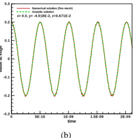
Since the interested ECR-CVD chamber is in cylindrical shape, a cylindrical cavity resonance test case with analytical solution is chosen to test the 3D Maxwell’s equation solver. Test conditions (Fig. 3) include: initial TM001 mode, ε0=8.854*1012 H/m, µ0=1.257*10-6 F/m, σ=0. S/m, f=1.983 GHz,
∆t=5.042*10-12 s, T=100∆t for one cycle, diameter=0.12 m and height=0.12 m. The cylindrical wall is considered as a perfect conductor. Only Ez component is nonzero in this test case.
Fig. 3a and Fig. 3b compare the time evolution of Ez (~ 4 cycles) at some point in the cylinder with analytical solution using coarse and fine mesh, respectively. Results show that the excellent agreement with analytical solution is found even with the use of coarse mesh.
Figs. 4a-4c, respectively, compare the spatial distribution of the computed Ez, Hx and Hy with those of analytical solutions at z=0 plane. Note that both data resulting from the coarse and fine meshes are included for comparison purpose. Results show that with this initial TM001-mode wave, only Ez component can sustain afterwards. Resulting Hx and Hy are found to be orthogonal to each other in Fig. 4b and Fig. 4c, as it should be. In general, computational results of the
spatial field distribution agree very well with analytical solution. The above validate the current development of the 3D Maxwell’s equation solver using edge-based finite element method.
4. CONCLUSIONS
In the second year of the current project, we have developed and verified a parallel PIC/MCC method using both 1D DC and RF argon gas discharge. Comparing to previous studies validates the current PIC/MCC code. In addition, a 3D Maxwell equation solver using edge-based finite element method is developed and verified by excellent agreement with analytical solution. Several works planned in the very near future are briefly summarized as follows:
1. To parallelize the Maxwell’s equation solver based on the previous experience in parallelization of the Poisson’s equation solver.
2. To include the Maxwell’s equation solver into the parallel PIC/MCC module.
3. To apply the above completed code to compute the methane/hydrogen plasma in the mid of the third year of the project.
References
1. 郭 正 次 : Fabrication and
characterizations of the alloy-encapsulated carbon nanostructures for applications in nano-resolution storage media and others. NSC 92-2120-M-009-001. 2. T. Makabe, Research Report 2000-2001,
Lab. Plasma Electronics, Keio University.
3. K. Nanbu, IEEE Plasma Science, Vol. 28 (2000), pp. 971-990.
4. Birdsall, C.K. and Langdon, A.B., Plasma Physics via Computer
Simulation, McGraw-Hill, New York, NY, USA, 1985.
5. Saad, Yousef, Iterative Methods for Sparse Linear Systems, PWS Publishing Company, International Edition, 1996.
Figure 1 Typical computational procedures for a
PIC/MCC simulation
(b)
(c)
(d)
(e)
(f)
Figure 2 Simulated property distribution of RF gas
discharge (50 mtorr, 500 V, 20 mm, 13.56 MHz). (a) Potential (b) electric field (c) number density (d) average kinetic energy (e) EEDF (f) EEDF (20 mtorr).
X -0.05 0 0.05 Y -0.05 0 0.05 z 0 0.05 0.1
Figure 3 Unstructured tetrahedral mesh for the
simulation of cylindrical cavity resonance (TM010,
f=1.983 GHz, perfect conductor wall) (coarse: 40238 elements, fine: 227603 elements)
time v a lu e a t e d g e
0 5E-10 1E-09 1.5E-09 2E-09
-1 -0.8 -0.6 -0.4 -0.2 0 0.2 0.4 0.6 0.8 1
Numerical solution (coarse mesh) Analytic solution x= 8 2.73E-02, y=0.0, z=3.469E-02
time v a lu e a t e d g e
0 5E-10 1E-09 1.5E-09 2E-09
-0.3 -0.2 -0.1 0 0.1 0.2 0.3
Numerical solution (fine mesh) Analytic solution x= 0.0, y= -4.918E-2, z=6.671E-2
(b)
Figure 4 Comparison of time evolution of electric
field in the x-direction between simulation and analytical solution. (a) coarse mesh (b) fine mesh.
X -0.06 -0.04 -0.02 0 0.02 0.04 0.06 Y -0.06 -0.04 -0.02 0 0.02 0.04 0.06 1 44 1 7 2 3 5 11 7 2 2 5 8 2 7 4 7 6 3 5 5 7 3 11 1 1 2 7 3 7 9 4 4 4 4 1 1 7 9 5 4 8 2 9 8 2 8 7 4 4 5 4 5 6 9 1 1 9 1 1 1 2 3 1 3 6 6 4 6 4 4 5 1 8 1 1 8 1 2 2 5 3 8 2 7 7 4 4 8 7 2 4 6 2 1 4 1 5 3 2 2 3 3 4 5 Level Ez 9 0.3000 8 0.2650 7 0.2300 6 0.1950 5 0.1600 4 0.1250 3 0.0900 2 0.0550 1 0.0200 LevelREz 9 0.3000 8 0.2650 7 0.2300 6 0.1950 5 0.1600 4 0.1250 3 0.0900 2 0.0550 1 0.0200 Green Line----Analytic solution
Blue Line----Numerical line (fine mesh, 22410 nodes)
Red Line----Numerical line (coarse mesh, 8226 nodes)
(a) X -0.06 -0.04 -0.02 0 0.02 0.04 0.06 Y -0.06 -0.04 -0.02 0 0.02 0.04 0.06 8 7 11 8 10 9 9 11 4 5 5 4 2 4 6 1 2 5 1 2 3 55 3 2 4 6 1 4 10 7 11 1 0 7 11 9 8 10 10 11 8 7 11 Level Hx 11 0.0014 10 0.0011 9 0.0008 8 0.0006 7 0.0003 6 -0.0000 5 -0.0003 4 -0.0006 3 -0.0008 2 -0.0011 1 -0.0014 LevelRHx 11 0.0014 10 0.0011 9 0.0008 8 0.0006 7 0.0003 6 -0.0000 5 -0.0003 4 -0.0006 3 -0.0008 2 -0.0011 1 -0.0014 Green Line----Analytic solution
Blue Line----Numerical line (fine mesh, 22410 nodes)
Red Line----Numerical line (coarse mesh, 8226 nodes)
(b) X -0.06 -0.04 -0.02 0 0.02 0.04 0.06 Y -0.06 -0.04 -0.02 0 0.02 0.04 0.06 3 1 4 5 3 2 11 1 0 7 7 1 010 8 7 9 7 9 8 6 5 3 4 5 4 1 4 8 10 6 9 11 2 3 6 6 5 5 3 2 6 7 11 11 Level Hy 11 0.0014 10 0.0011 9 0.0008 8 0.0006 7 0.0003 6 -0.0000 5 -0.0003 4 -0.0006 3 -0.0008 2 -0.0011 1 -0.0014 Level Rhy 11 0.0014 10 0.0011 9 0.0008 8 0.0006 7 0.0003 6 -0.0000 5 -0.0003 4 -0.0006 3 -0.0008 2 -0.0011 1 -0.0014 Green Line----Analytic solution
Blue Line----Numerical line (fine mesh, 22410 nodes)
Red Line----Numerical line (coarse mesh, 8226 nodes)
(c)
Figure 5 Comparison of spatial distribution between
simulation and analytical solution for the cylindrical
行政院國家科學委員會專題研究計畫成果報告
奈米解析度記錄媒體及其他應用之包覆合金碳奈米結構陣列,其
製造、機械/熱性質及製程特徵之研究子計畫三(2/3)-奈米結構
沉積製程與積體電路製程之整合
計畫編號:92-2120-M-009-008-
執行期限:2004 年 08 月 01 日至 2005 年 07 月 31 日
主持人:潘扶民 國立交通大學材料科學與工程研究所
中文摘要 我們本計畫的第二年度內的主要研究 內容為:(1) 以製作陽極氧化鋁(anodic aluminum oxide, AAO)自組裝奈米孔洞陣列結構做為版模,在矽基材製作 TiO2奈米 點三極體結構;(2)以 AAO 奈米孔洞陣列 結構做為版模開發奈米碳管(carbon nanotube, CNT) 選區成長與控制碳管濃度 製程技術。利用奈米點作為電子發射源製 作場效發射三極體元件,此場效發射三極 體擁有 45 伏特之低閘極啟始電壓,且在 120 伏特的閘極電壓下,場效發射電流密 度高達 25 毫安培/平方公分。此奈米點之 電子發射源具有低製成溫度與極佳的均勻 性等優點,將可滿足大面積場效發射顯示 器之製程需求。奈米碳管的成長受到奈米 孔洞的限制與外加偏壓或電漿自我偏壓的 影響,因此具有極佳的垂直準直性。藉由 調整甲烷與氫氣之反應氣體比例即可有效 地控制奈米碳管成長出奈米孔洞外之管束 密度。 關鍵詞:陽極氧化鋁、碳奈米管、場效發 射三極體、啟始電壓 Abstract
We have carried out two research tasks in the second project year: (1) fabrication of triode-type field emission structure using the titanium oxide nanodot arrays on silicon substrate using the AAO as the template; (2) tunable tube density of CNTs grown from the AAO nanopores. A field emission triode device using the self-organized nanodot arrays as electron emission source was
proposed and fabricated. The field emission triodes exhibited a low gate turn-on voltage of 45 V and high emission current density of 25 mA/cm2 at 120 V. The desirable electric properties and easily controllable fabrication process of the nanodot triodes show potential for application in field emission displays and vacuum microelectronics. Ordered arrays of CNTs were prepared by using the AAO films as templates and the segments of CNTs stretching out of the AAO nanopores still maintain relatively good alignment. We have also demonstrated that the tube number density of aligned CNTs grown over the AAO template can be directly controlled by adjusting the CH4/H2 feed ratio during the CNT growth.
Keywords
anodic aluminum oxide (AAO), carbon nanotube (CNT), field emission triode, turn-on voltage
1. Introduction
Cold-cathode field emitter arrays (FEAs) have been the subject of intense research, primarily because of potential applications for many technologies, such as field emission flat panel displays, cold-cathode microwave devices, and electron guns in the x-ray tubes. For practical applications, FEAs must have a low turn-on voltage, high emission current density, high current stability, and a long lifetime. In the past decade, numerous nanostructured materials, including carbon nanotubes (CNTs),1-3
carbon nanoparticles (CNPs),4 IrO2
nanorods,5 ZnO nanowires,6,7 MoS2
17
studied to achieve the goal.
In our previous studies, we used nanoporous anodic aluminum oxide (AAO) films as the mask for local anodic oxidation of metal films to fabricate nanodot arrays of metal oxides.9,10By using the AAO mask as
the anodization template for metallic thin films, one can produce ordered arrays of oxide nanodots with a very high packing density (as high as 1010 cm-2) and a uniform
size distribution. In addition, the thus fabricated nanodots of metal oxides provide stable chemical and microstructure properties, whereas metallic FEAs (e.g., molybdenum and niobium tips) have shown increasing tendency to oxidation under normal operation conditions, resulting in emission current fluctuation.11,12Tatarenko et
al.13have demonstrated that oxide nanodots
with a high geometrical enhancement have a high field emission efficiency. In order to study the feasibility of integration of the nanodot arrays into conventional integrated circuit (IC) process technology for field emission applications, we have fabricated the triode-type field emission structure using the titanium oxide nanodot arrays as the cold cathode.
The second part of our work is to use CNTs as another field electron emitter material. For field mission display application, it is necessary to grow vertically aligned CNT arrays on a large area with suitable tube density and tube dimensions. In recent years, template methods, such as AAO nanotemplates in particular, have been widely introduced to produce well aligned and monodispersed CNT arrays.14 We report
that the tube density of the cobalt-catalyzed CNTs on the AAO template can be controlled by regulating the flow rate ratio of methane (CH4) to hydrogen (H2) precursor gases during the CNT growth, and thereby field emission characteristics of CNTs can be adjusted.
2. Experimental
(1) Triode-type field emission structure using the titanium oxide nanodot arrays
Figure 1 illustrates the fabrication process of nanodot-based field emission triodes. Figs. 1a-1c show the preparation steps of the nanodot emitter, and Figs. 1d-1i show the fabrication steps of the triode structure. At first, as-deposited Al/Ti film stack are oxidized by electrochemical anodization. The AAO templated nanodots have an average diameter of about 40 nm and an average height of about 30 nm and then annealed at 450oC in a high vacuum furnace for 2 hour. A dielectric layer of tetraethoxysilane (TEOS) oxide layer and a titanium layer were directly deposited onto the nanodot array respectively. The gate aperture array with a diameter of 20 µm was defined on the titanium layer with a photolithography system and etched by Reactive ion etching (RIE). After the RIE, the sample was dipped into a dilute HF solution for a few seconds to sweep away the residual TEOS oxide on nanodots in the triodes. In the final step, the photoresist was removed by acetone (Fig. 1i) and fabrication of the nanodot triodes was completed. The field emission properties of the triode devices were characterized by electrical microprobes equipped in a FE-SEM system with a base pressure of 10-7Torr.
(2) Tunable tube density of CNTs grown from the AAO nanopores
Ordered AAO pore channel arrays were prepared by two-step anodization and the Co
catalyst for the CNT growth was
electrochemically deposited at the pore bottom. The CNT growth was carried out in the electron cyclotron resonance chemical deposition (ECR-CVD) system. The gas mixture of CH4 and H2 was used as the carbon source carbon source and the total gas flow rate was kept constant at 22 sccm. The CH4 concentration in the gas precursor was varied from 9% to 91% in order to investigate the influence of the CH4/H2 ratio on the CNT growth.
The field emission measurements were conducted by the simple diode configuration and performed in a vacuum about 10-6 Torr. The anode is a platinum wire with a
18
hemispherical tip 1 mm in diameter. The distance between the CNTs and the anode was about 100 µm.
3. Results and Discussion
(1) Triode-type field emission structure using the titanium oxide nanodot arrays
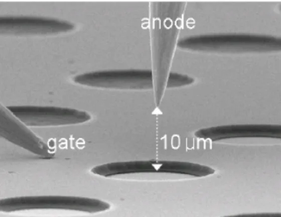
In order to study the feasibility of integration of the nanodot arrays into conventional integrated circuit (IC) process technology for field emission applications, we have fabricated the triode-type field emission structure using the titanium oxide nanodot arrays as the cold cathode. A side-view SEM image of the triode arrays is shown in Figure 2a. The triode sample contains 16×16 arrays of gated cathode cells. Fig. 2b shows a higher magnification image of the nanodot emitter arrays inside the gate aperture. The SEM image clearly shows that the titanium oxide nanodot arrays maintain their geometrical configuration without discernable damage after the dilute HF dip and the RIE processes. This demonstrates the feasibility of fabrication of nanodot-based field emission devices using standard microfabrication techniques. The microprobes can be manipulated by piezo-driven linear nanomotors with a minimum step size of 10 nm in the x-y-z directions. Figure 3 is the in situ SEM image showing the configuration of field emission measurement for a triode using tungsten microprobes. The cathode (nanodot emitters) was grounded and the gate electrode was connected to the microprobe with the positive bias sweeping from 0 to 120 V. The field emitted electrons were collected by a microprobe (anode), which was about 10 µm away from the gate aperture and biased with +50 V. Since the triode cells were well separated, this measurement configuration allowed us to measure the field emission properties of individual gated cathode cells by the microprobes. The supply of the dc bias and field emission measurement were performed with high voltage
source-measurement units (Keithley 237). Figure 4 shows the gate-voltage dependence of the emission current of the nanodot triodes. The electron emission started at the gate voltage of about 45 V, and the anode current exceeded 80 nA when the gate voltage was increased to 120 V. Because the measured anode current was mainly provided by one single cathode cell (gate aperture) under the anode probe, the anode current of 80 nA measured at a gate voltage of 120 V corresponds to an emission current density of 25 mA/cm2(one aperture area ~
3×10⁻⁶cm2). As compared the field emission
result of the cathode cells with one another, little difference was observed, suggesting an excellent distribution uniformity of nanodot emitters in the triodes. The F-N plot of the anode current shown in the inset of Fig. 4 also exhibits a linear F-N fit, confirming that the field emitted electrons extracted by the gate bias was responsible for the measured anode current. Although the titanium oxide nanodots in the triodes show satisfactory field emission characteristics, the current leakage from the emitters to the gate electrodes was large. The measured gate current is about 50% of the anode current as shown in Fig. 4. The detection of the high gate current is owing to that the whole 16×16 arrays of gated cathode cells are biased by the same gate electrode, and leakage currents of all the cathode cells were, therefore, measured simultaneously. In contrast, the anode current was practically measured from only one cathode cell.
(2) Tunable tube density of CNTs grown from the AAO nanopores
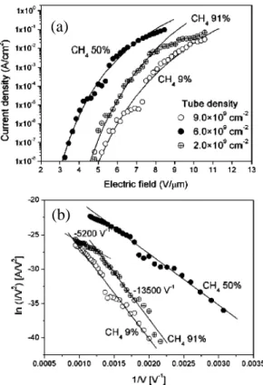
Figures 5(a)–5(c) show the side-view SEM of the AAO templated CNTs grown at CH4 concentrations of 9%, 50%, and 91%, respectively. At the CH4 concentration of 9% (see Fig. 5(a)), the tube density of CNT is as high as 9.0×10⁹tubes/cm2, indicating a
pore-filling ratio of about 82%, which is defined as the density ratio of the nanotubes to the AAO pores. At an extremely high CH4 concentration of 91% (see Fig. 5(c)), the
19
tube density decreases significantly to about 2.0×10⁹ tubes/cm2, corresponding to a
pore-filling ratio of about 18%. The inset in Fig. 5(b) shows the transmission electron microscopy (TEM) image of the CNTs. It clearly shows that a Co catalyst particle is encapsulated at the tube tip and covered by graphitic cap, suggesting that the CNT growth is via the tip-growth mechanism.15
During the CNT growth in the CH4/H2 plasma, the a-C by-product is concurrently deposited on the AAO template, and the a-C deposition seems to play an important role in control of the tube density of CNTs on the AAO template whereas it can be quickly etched away by reactive hydrogen species in the plasma.16 At a high CH
4/H2 feed ratio, the a-C deposition overwhelms the etch reaction, resulting in steady growth of the
a-C.17 The a-C layer will gradually cover up
the AAO nanopores and prevent nanotubes from growing out of the nanopores. As shown in the inset of Fig. 5(c), some short nanotubes marked by white arrows are buried inside the nanopores. Those CNTs which have already grown out of the nanopores can continuously grow up since the CNT growing site is at the tip of the nanotubes stip-growth mechanismd. At the CH4 concentration of 91%, only about 18% of CNTs grew out of the AAO nanopores. On the other hand, at a low CH4/H2 feed ratio, the AAO surface is almost free from the a-C layer (see the inset of Fig. 5(a)) since it was quickly etched away by hydrogen species, leading to efficient CNT growth and thus a very high tube density. Figure 5(d) shows that the tube density is inversely proportional to the CH4 concentration. In addition to the tube density, the CNTs grown at CH4 concentration of 91% are shorter than those grown at 50% and 9% as shown in Figs. 5(a)-(c). This is probably due to that the a-C layer may also be deposited on the CNT, which can hinder reactive carbonaceous species from reaching the Co catalyst, hence reducing the CNT growth rate.
4. Conclusions
In summary, field emitter arrays of titanium oxide nanodots were prepared on the silicon wafer by electrochemical anodization of the titanium thin film in terms of AAO templation. Fabrication of the field emission triodes is compatible with conventional IC technology. Field emission properties of individual gated cathode cells have been studied using electrical microprobes in an FE-SEM system, and a low gate turn-on voltage of 45 V and considerably high emission current density of 25 mA/cm2 at 120 V were measured. The tube number density of aligned CNTs grown over the nanoporous AAO template can be directly controlled by adjusting the CH4/H2 feed ratio during the CNT growth. A high CH4 concentration leads to the heavy deposition of an a-C deposit on the AAO surface. Although the a-C can effectively decrease the CNT density on the AAO template, thereby decreasing the field-screening effect and increasing the field enhancement, it notably deteriorates the electron field emission property of the CNTs. The nonlinearity of the F–N plot of the CNTs is ascribed to the deposition of the
a-C overlayer on the CNT tip. The CNTs
grown at 50% CH4 show the best field emission property.
References
1. Walt A. de Heer, A. Châtelain, and D. Ugarte, Science, 270, 1179 (1995).
2. Yahachi Saito and Sashiro Uemura, Carbon, 38, 169 (2000).
3. Jean-Marc Bonard, Jean-Paul Salvetat, Thomas Stöckli, Walt A. de Heer, László Forró, and André Châtelain, Appl. Phys. Lett., 73, 918 (1998).
4. Kyung Ho Park, Hyung Jun Han, Seungho Choi, Kyung Moon Lee, Soonil Lee, and Ken Ha Koh, J. Vac. Sci. Technol. B, 21, 562 (2003).
5. Reui-San Chen, Ying-Sheng Huang, Ya-Min Liang, Chim-Sung Hsieh, Dah-Shyang Tsai, and Kwong-Kau Tiong, Appl. Phys. Lett., 84, 1552 (2004).
20
6. Yung-Kuan Tseng, Chorng-Jye Huang, Hsin-Min Chen, I-Nan Lin, Kuo-Shung Liu, and I-Cherng, Adv. Funct. Mater., 13, 811 (2003).
7. S. H. Jo, J. Y. Lao, Z. F. Ren, R. A. Farrer, T. Baldacchini, and J. T. Fourkas, Appl. Phys. Lett., 83, 4821 (2003).
8. Y. B. Li, Y. Bando, and D. Golberg, Appl. Phys. Lett., 82, 1962 (2003).
9. Po-Lin Chen, Cheng-Tzu Kuo, Tzeng-Guang Tsai, Bo-Wei Wu, Chiung-Chih Hsu, and Fu-Ming Pan, Appl. Phys. Lett., 82, 2796 (2003).
10. Po-Lin Chen, Cheng-Tzu Kuo, Fu-Ming Pan, and Tzeng-Guang Tsai, Appl. Phys. Lett., 84, 3888 (2004).
11. S. Itoh, T. Niiyama, and M. Ykoyama, J. Vac. Sci. Technol. B, 11, 647 (1993). 12. B. R. Chalamala, R. M. Wallace, and B. E. Gnade, J. Vac. Sci. Technol. B, 16, 2859 (1998).
13. N. I. Tatarenko, V. A. Solntsev, and A. N. Rodionov, J. Vac. Sci. Technol. B, 17, 647 (1999).
14. J. Li, C. Papadopoulos, J. M. Xu, and M. Moskovits, Appl. Phys. Lett. 75, 367 (1999). 15. R. T. K. Baker, Carbon 27, 315 (1989). 16. Olivier M. Küttel, Oliver Groening, Christoph Emmenegger, and Louis Schlapbach, Appl. Phys. Lett. 73, 2113 (1998).
17. K. B. K. Teo, M. Chhowalla, G. A. J. Amaratunga, W. I. Milne, G. Pirio, P. Legagneux, F. Wyczisk, J. Olivier, and D. Pribat, J. Vac. Sci. Technol. B 20, 116 (2002).
21
Figure 1. Fabrication steps for the TiO2 nanodot-based field emission triodes. (a) Ti and Al deposition, (b) anodization, (c) AAO removal and vacuum annealing, (d) TEOS oxide deposition, (e) Ti deposition, (f) photoresist pattern formation, (g) dry etching of Ti, (h) dry etching of TEOS oxide, and (i) lift-off the photoresist.
Figure 2. (a) Side-view FE-SEM image of the
nanodot-based field emission triode array. The inset shows the enlarged image of a triode. (b) Side-view FE-SEM image of the TiO2 nanodot emitters in the triode.
Figure 3. FE-SEM image of the field emission
measurement configuration for a triode device. The tip of anode microprobe is about 10 µm away from the gate electrode.
Figure 4. Gate-voltage dependence of the
anode and gate current of the triode. The inset shows the corresponding Fowler-Nordheim plot of the anode current.
Figure 5. Side-view SEM images of the AAO
templated CNTs grown at CH4 concentrations of (a) 9%, (b) 50%, and (c) 91%. The insets in (a) and (c) are the cross-sectional view of the CNTs. The inset in (b) is the TEM image of the
22
CNT. (d) The tube density of CNTs grown over the AAO nanopores as a function of the CH4 concentration.
Figure 6. (a) Field emission current density (J)
as a function of electric field (E) for the CNTs grown on the AAO template with the three different tube densities shown in Figs. 5(a)–(c). The solid curves are F–N fits using the low current/field regions which do not show saturation. (b) Corresponding F–N plots of data. The slopes of the F–N plot for the CNTs grown at 91% CH4 are also indicated in the figure
(a)