國
立
交
通
大
學
應用化學研究所
博
士
論
文
奈米結構增強之有機電激發光二極體材料及元
件研究
Nano-Structure Enhanced Organic Light Emitting
Materials and Devices
研 究 生:陳奎百
指導教授:許千樹 教授
奈米結構增強之有機電激發光二極體材料及元件研究
Nano-Structure Enhanced Organic Light Emitting Materials
and Devices
研究生:陳奎百 Student : Kuei-Bai Chen 指導教授:許千樹 教授 Advisor : Prof. Chain-Shu Hsu
國立交通大學
應用化學研究所
博士論文
A Thesis
Submitted to Insitute of Applied Chemistry National Chiao Tung University
in Partial Fulfillment of the Requirements for the Degree of Ph.D.
in
Applied Chemistry September 2005
Hsinchu, Taiwan, Republic of China
奈米結構增強之有機電激發光二極體材料及元件
研究
研究生:陳奎百 指導教授:許千樹 教授
國立交通大學應用化學研究所
摘要
本研究主要目的在於探討導入不同之奈米粒子於發光分子中,在有機 發光二極體元件中之表現。藉由化學鍵結之方式與奈米粒子結合,並利用 奈米粒子之特性來增進元件之效率。本研究依不同之奈米粒子分成三部份 加以探討,第一部份為導入多面體矽氧烷之奈米粒子,第二部份則導入金 奈米粒子,第三部份則導入硒化鎘/硫化鋅奈米晶粒。 第一部份合成出八種發光基單體,其中兩種為 OPV 衍生物的螢光分子 (C-1 ~ C-2);一種為銥錯合物的磷光分子(C-3) ; 五種為高分子(P1~P5)。相 較於發光基單體,以 POSS 為中心核的星狀發光結構可以改善材料之熱性 質,使熱穩定性增加,並降低分子鏈的移動。星狀發光材料的 UV-PL 光譜 及電化學性質皆與發光基單體相似,並不會因 POSS 引入的影響而造成光色 的偏移,且於不同媒介下,星狀材料之光色穩定度較發光單體佳。此外, 由室溫~200℃的溫度下進行迴火(annealing)實驗,其研究結果顯示,星狀發 光材料 POSS1~POSS3 及 POSSP1~POSSP5 之吸收及放射光譜皆明顯較發光 單體 C-1~C-3 及 P1~P5 穩定。WAXD 的結果顯示,中心核 POSS 之晶格結 構因發光單體的引入而有些許改變(d-spacing 變大),不過星狀發光材料仍因 含有 POSS 而具有奈米尺寸的晶格結構。 POSS1~POSS3 屬於藍綠~黃綠的發光材料。由於其具有一定的成膜 性,故可直接以旋轉塗佈的方式製成元件。將此星狀發光材料製成單層的有機電激發光元件,POSS 1、POSS 2 混入 PVK:PBD 的元件亮度分別為 1102 cd/m2及 1468 cd/m2,效率接近 1 cd/A;POSS 3 以 CPB 為主體,LiF 做為陰 極修飾層,亮度可達 1458 cd/m2。將 POSS 3 元件加入 TPBI 做為電洞阻擋 層後,效率可增加至 3.99 cd/A。此外,星狀發光材料之元件於不同電壓下 皆仍維持穩定的 EL 光譜。而 POSSP1~POSSP5 亦由於含有 POSS 中心核, 其亮度及效率皆有所提升。 第二部份則合成一含硫醇之發光單體(S-1),並利用金奈米粒子含量之 不同合成出 Au-1 及 Au-2。利用 FT-IR,NMR 及 TGA 可確定發光單體已成 功的鍵結於金奈米粒子上。實驗結果顯示其溶液狀態下最大吸收波長為 431nm,最大放射波長為 497nm,和發光單體相同。其螢光發光效率由 0.32 提升至 0.47 在 Au-1 及 0.53 在 Au-2。 在元件之製作上,其元件架構為 ITO/PEDOT/Au-n/Ca/Al,並分別製作 發光分子摻混金奈米粒子及發光分子鍵結金奈米粒子兩種元件,在掺混元 件中,發光基團選用不含硫醇基團但具有相同發光基團之 C-2,避免不必要 之化學反應,實驗中最好之掺混比例為 1:0.0625(C-2:Au),其亮度可到達 1071 cd/m2,效率可到達 0.67 cd/A。隨著掺混比例之增加,其效率反而降低。 Au-1 之最大亮度可提升至 2010cd/m2,最大效率可提升至 1.4cd/A,同樣隨 著金奈米粒子導入量之增加,Au-2 效率反而下降至 0.39cd/A。而比較兩種 元件,可發現發光分子鍵結金奈米粒子有較好之元件表現。 第三部份則合成三種含 sulfide 基團之發光高分子(S1PPV~S3PPV),並 利用 ligand exchange 來包覆 CdSe/ZnS 奈米晶粒。並利用 FT-IR,GPC,TEM 及 TGA 來確定發光分子已成功的包覆於 CdSe/ZnS 上。這些發光高分子之 放射波長大約介於 540~555nm 間,且包覆上奈米晶粒後,其光色並沒有改 變。測量其循環伏安計量,發現其能階亦同樣並不因奈米晶粒的導入而有 所改變。 在元件之製作上,分別製作單純發光分子,發光分子摻混 CdSe/ZnS 奈 米晶粒及發光分子包覆 CdSe/ZnS 奈米晶粒三種。在 S1PPV 之系列中,其 最大亮度約為 8285 cd/m2,最大效率為 0.79 cd/A,在掺混 CdSe/ZnS 之元件
中為 8158 cd/m2,最大效率為 0.86 cd/A。當包覆 CdSe 後,其最大亮度可增 加為 15960 cd/m2,最大效率為 1.47cd/A。在 S2PPV 中,經由包覆 CdSe/ZnS, 亮度可由 3225 cd/m2到達 14470 cd/m2,效率可由 0.95 cd/A 到達 1.85 cd/A。 在 S3PPV 中亮度可由 6073 cd/m2到達 13390 cd/m2,效率可由 0.82 cd/A 到 達 2.25 cd/A。而比較三種元件,可發現利用包覆 CdSe/ZnS 之發光材料,可 得到最好之元件表現。
Nano-Structure Enhanced Organic Light Emitting
Materials and Devices
Student:Kuei-Bai Chen Advisor:Prof. Chain-Shu Hsu
Institute of Applied Chemistry
National Chiao Tung University
Abstract
The goal of this research is to study the performance of organic light emitting diodes via incorporating different kinds of nanoparticles. We incorporate the nanoparticles by using chemical bonding and enhance the device performance via the character of nanoparticles. Three kinds of nanoparticles are chosen for this study. The first part of this study was focused on the synthesis of light emitting materials using Polyhedral Oligomeric Silsesquioxane(POSS) as a core. The second part of this study was focused on chromophore bonding with gold nanoparticle. The third part of this study was focused on PPV type polymers incorporating with CdSe/ZnS nanocrystals.
In the first part of this study, we have synthesized eight novel light emitting materials (POSS1~POSS3, POSSP1~POSSP5), which utilize polyhedral oligomeric silsesquioxanes (POSS) as the core to link the chromophore, where the chromophores can be fluorescence (C-1,C-2), phosphorescence (C-3) dyes and polymer (P1~P5). Compared with the corresponding chromophores, the incorporation of the silsesquioxane core could enhance the thermal stability and reduce the chain mobility. POSS1~POSS3 and POSSP1~POSSP5 have similar absorption and photoluminescent spectra. The silsesquioxane core does not
affect the energy gap of light emitting materials. The annealing experiments show that the PL spectral stabilities of star-like light emitting materials are better than those of chromophores. These results show that the incorporation of the silsesquioxane core could enhance the thermal and luminescent stabilities. WAXD results show that although the crystal structure of the silsesquioxane core is affected by the chromophores, POSS1~POSS3 and POSSP1~POSSP5 still keep nanoscale crystal structures.
POSS1~POSS3 emit blue-green to yellow-green light. The star-like light emitting materials show good film forming property. Therefore they can be used to fabricate devices by a spin coating process. The single-layer LED devices (ITO/PEDOT/POSSn:PVK:PBD/Ca/Al) of POSS 1, POSS 2 show maximum
brightness of 1102 cd/m2 and 1468 cd/m2 respectively; maximum quantum
efficiency is 1 cd/A. The maximum brightness of the device
(ITO/PEDOT/POSS3:CBP/LiF/ Ca/Al) is 1458 cd/m2. After blending TPBI as
the hole blocking material, the maximum quantum efficiency can be increased up to 3.99 cd/A. In addition, the EL spectra are stable even at high voltages. POSSP1~POSSP5 also show higher luminance and quantum efficiency because they contain POSS as cores.
In the second part of this study, a thiol containing chromophore (S-1) was synthesized. The chromophore S1 was linked with different amounts of gold nanoparticles via thiol group to form the gold nanoparticle containing chromophore Au-1 and Au-2. Both Au-1 and Au-2 were measured by FT-IR, NMR, and TGA to make sure that chromophore S1 was linked with the gold nanoparticles. The Au-1 and Au-2 show an UV absorption peak at 431 nm and a PL emission peak at 497 nm. Both values are the same with those of chromophore S-1. However, the PL quantum efficiencies of Au-1 and Au-2 are enhanced to reach 0.47 and 0.53 respectively.
PEDOT/Au-n/Ca/Al. The Au-1 devices shows the maximum luminance of 2010
cd/m2 and maximum EL quantum efficiency of 1.4 cd/A while Au-2 device
exhibits the maximum luminance of 896 cd/m2 and EL quantum efficiency of
0.39 cd/A. For comparison, we also fabricate the devices using C-2 blending with gold nanoparticle as the emitting layer. The reason we choused C-2 is it contains the same chromophore and no thiol group to prevent any chemical
reaction. The best device shows the luminance of 1071 cd/m2 and maximum
quantum efficiency of 0.67 cd/A. In this device, the weight ratio of C-2 and gold nanoparticles is 1:0.0625. The results demonstrate that the chromophore linked with the gold nanoparticles has much better EL device performance than the chromophore blending with gold nanoparticles.
In the third part of this study, three sulfide group-containing light emitting polymers (S1PPV-S3PPV) were synthesized. The sulfide group-containing polymers were used to tether the CdSe/ZnS nanocrystals via ligand exchange reaction. The obtained CdSe/ZnS nanocrystal and SnPPV composites were characterized by FT-IR, NMR, GPC, TGA and TEM. The results demonstrate that CdSe/ZnS nanocrystals are uniformly dispensed in the SnPPV matrix. The PL emissions of these composites reveal in the range from 540~550 nm which is similar to those of the original SnPPV. The cyclic voltametry measurements also show that the energy band gaps of the composites are the same with those of their corresponding SnPPV polymers.
Three kinds of devices based on the original SnPPV, SnPPV-CdSe composite and blending of CdSe/ZnS and SnPPV have been fabricated. The
S1PPV device show the maximum luminance of 8285 cd/m2 and maximum
yield of 0.79 cd/A. For the blending device, its maximum luminance and yield
are 8185 cd/m2 and 0.86 cd/A respectively. For S1PPV-CdSe composite device,
both maximum luminance and yield increase dramatically to reach 15960 cd/m2
systems. The maximum luminance and yield of S2PPV and S3PPV are 3225
cd/m2 and 0.95 cd/A, and 6073 cd/m2 and 0.82 cd/A respectively. However, the
S2PPV-CdSe and S3PPV-CdSe composite devices exhibit the maximum luminance and yield of 14470 cd/m2 and 1.85 cd/A and 13390 cd/m2 and 2.25 cd/A. All these results demonstrated that the device based on the SnPPV-CdSe composite have much better EL performance than those of the original SnPPV and blending of SnPPV with CdSe/ZnS nanocrystals.
謝誌
首先,最應該感謝的,就是我的指導教授許千樹教授,老師於五 年多來的研究其間孜孜不倦的給予我指導與教誨,尤其是對於我人生 方向的指引更是讓我受益良多。 特別感謝周卓輝教授、陳文章教授、韋光華教授、孟心飛教授對 於我論文的不吝指教,使得這篇論文更趨完整。 在這個充滿溫馨的實驗室,感謝勝雄學長在各方面的一路扶持, 如果沒有他的幫助,我也沒有這些實驗的成果。感謝亮仁學長在有機 合成方面知識的協助,感謝智文、阿慶及君豪於博愛蒸鍍實驗的幫 忙,不過也希望阿慶不要再碎碎唸了。感謝助理小燕在實驗室生活中 的幫助,感謝羅比、大楠及軍浩總是帶動實驗室歡樂的氣氛,讓我的 研究生活不感到苦悶。不過軍浩,下次講故事,還是講重點比較好, 以免大家都聽不懂。銘慧(大 pay)、佩萱(小 pay)及又加學妹幸虧有了 妳們,在這個以男生居多的實驗室裡增添了溫柔的氣氛。尤其是銘慧 這位”美女”,感謝你在實驗上的幫忙。感謝永鑫、敏碩、晉彥、永明、 韋伯、建宏、chetan 在研究期間給予的協助,實驗室的新成員迪迪、 小毛、怡碩看你們認真的投入研究中,感覺到實驗室充滿了希望。可 是小毛,在牙套還沒拿下來前,還是不要用正臉和人說話,以免口水 又噴到別人了。至於已經畢業的阿太、志偉、鐘毅、敏華、興銓、育 南、月泙、建呈、建凱、弘益、湘盈、杰修、信嵐,感謝你們在我研 究上的幫助,祝你們在事業上都有優秀的發展,尤其感謝月泙和弘 益,論文中有一部份也是和你們一起努力的成果。當然,最應該感謝 的,是每天幫我買飯的欣怡,要不是她,我大概早就餓死了吧。 最後感謝一路對我不離不棄支持我、陪伴我的家人,謹以此論文 獻給我所敬愛的父母親。目 錄
頁次 審定書 授權書 中文摘要 ……… i 英文摘要 ……… iv 謝誌 ……… viii 目錄 ……… ix Scheme 目錄 ……… xiii 表目錄 ……… xiv 圖目錄 ……… xv 第一章 緒論……… 1 1.1 有機電激發光元件之基本原理簡介……… 1 1.2 有機電激發光機制……… 5 1.3 對苯二乙烯衍生物於光化學上的應用……… 7 1.4 磷光元件之發展……… 8 1.5 聚對苯乙烯(poly(p-phenvylene vinylene))於發光元件上之應 用……… 10 1.6 聚芴(polyfluorene)於發光元件上之應用……… 12 1.7 奈米粒子之簡介……… 14 1.8 奈米材料在有機發光二極體元件上的應用……… 18 1.9 多面體矽氧烷寡聚物(POSS)材料的發展……… 19 1.10 金奈米粒子的發展及特性……… 21 1.11 硒化鎘奈米粒子的發展及特性……… 23 第二章 研究動機……… 28 第三章 實驗部份……… 29 3.1 試藥……… 29 3.2 測試儀器……… 293.2.1 核磁共振光譜儀( Nuclear Magnetic Resonance,NMR )…… 29
3.2.2 微差掃描卡計( Differential Scanning Calorimeter,DSC )…… 29
3.2.3 熱重分析儀( Thermal Gravimetric Analyzer,TGA )………… 29
3.2.4 傅立業紅外光光譜儀 (Fourier Transform Infrared Spectroscopy,FTIR)……… 30 3.2.5 凝膠滲透層析儀( Gel Permeation Chromatography,GPC )… 30
3.2.6 紫外線與可見光譜儀 ( UV-Vis Spectrophotometer )……… 30
3.2.7 螢光光譜儀(Luminescence Spectrophotometer)……… 30
3.2.8 循環伏安計量儀( Cyclic Voltammetry,CV )……… 31
3.2.9 OLED 元件性質的量測……… 31
3.2.10 掃描式電子顯微鏡(Scanning Electron Microscopy,SEM)… 31 3.2.11 廣角 X 光繞射儀(Wide Angle X-ray Diffraction,WAXD)… 31 3.2.12 薄膜測厚儀(surface profile,α-step) ……… 31 3.3 合成部分……… 32 3.3.1 發光單體 C-1 ~ C-3 的合成……… 32 3.3.2 星 狀 分 子 P O S S 1 ~ P O S S 3 , P O S S P 1 ~ P O S S P 5 的 合 成……… 40 第四章 結果與討論……… 57 4.1 單體合成部份……… 57 4.1.1 螢光單體 C-1 和 C-2……… 57 4.1.2 磷光單體 C-3……… 57 4.2 星狀分子合成部份……… 58 4.3 星狀分子的結構鑑定……… 59 4.3.1 傅立業紅外光光譜儀鑑定……… 59 4.3.2 1H-NMR 鑑定……… 63 4.3.3 GPC 量測……… 64 4.4 熱性質分析……… 65
4.4.1 熱重分析儀 TGA(Thermal Gravimetric Analyzer)……… 65
4.4.2 微差熱分析儀 DSC(Differential Scanning Calorimeter)……… 65
4.5 光學性質……… 67 4.5.1 溶劑及薄膜的影響……… 67 4.5.2 PL 量子效率的量測……… 79 4.5.3 濃度的影響……… 79 4.5.4 迴火(annealing)的影響……… 82 4.6 電化學性質……… 95 4.6.1 循環伏安計量(Cyclic voltammetry) ……… 95 4.7 有機發光二極體元件製作與光電性質量測……… 106 4.7.1 ITO pattern 的製作……… 106 4.7.2 發光元件的結構……… 107 4.7.3 螢 光 星 狀 分 子 發 光 元 件 的 結 構 與 光 電 性 質 ( P O S S 1 及 POSS2)……… 108 4.7.4 磷 光 星 狀 分 子 發 光 元 件 的 結 構 與 光 電 性 質 (POSS3)……… 115 4.7.5 高 分 子 星 狀 分 子 發 光 元 件 的 結 構 與 光 電 性 質
(POSSP1~POSSP5)……… 123 4.8 星狀分子之奈米結構探討……… 133 4.8.1 廣角 X 光繞射儀……… 134 4.9 星狀分子之元件壽命測試……… 137 第五章 結論……… 140 第六章 研究動機……… 142 第七章 實驗部份……… 143 7.1 試藥……… 143 7.2 測試儀器……… 143 7.3 合成部分……… 143 7.3.1 發光單體 S-1 的合成……… 143 7.3.2 發光金奈米粒子 Au-1 及 Au-2 的合成……… 147 第八章 結果與討論……… 150 8.1 單體合成部份……… 150 8.1.1 螢光單體 S-1……… 150 8.1.2 發光金奈米粒子合成部份……… 150 8.2 金奈米粒子之結構鑑定……… 150 8.2.1 傅立業紅外光光譜儀鑑定……… 150 8.2.2 1H-NMR 鑑定……… 151 8.3 熱性質分析……… 151
8.3.1 熱重分析儀 TGA(Thermal Gravimetric Analyzer)……… 151
8.4 光學性質……… 154
8.4.1 紫外可見光譜與螢光光譜分析……… 154
8.5 電化學性質……… 157
8.5.1 循環伏安計量(Cyclic voltammetry) ……… 157
8.6 金奈米粒子之奈米結構探討……… 161
8.6.1 掃描式電子顯微鏡 (Scanning Electron Microscopy, SEM) ……… 161 8.7 有機發光二極體元件製作與光電性質量測……… 162 8.7.1 ITO pattern 的製作及發光元件的結構……… 162 8.7.2 光電性質……… 162 第九章 結論……… 169 第十章 研究動機……… 171 第十一章 實驗部份……… 172 11.1 試藥……… 172 11.2 測試儀器……… 172 11.3 合成部分……… 172 11.3.1 發光單體 M-1 之合成……… 172
11.3.2 發光高分子 S1PPV~S3PPV,S1PPV-CdSe ~S3PPV-CdSe 之 合成……… 174 第十二章 結果與討論……… 179 12.1 發光高分子合成部份……… 179 12.1.1 發光高分子 S1PPV~S3PPV 的合成……… 179 12.1.2 發光高分子 S1PPV-CdSe~S3PPV-CdSe 的合成……… 179 12.2 發光高分子之結構鑑定……… 181 12.2.1 1H-NMR 鑑定……… 181 12.2.2 傅立業紅外光光譜儀鑑定……… 182 12.2.3 GPC 量測……… 184 12.2.4 穿透式電子顯微鏡(TEM)分析……… 186 12.3 熱性質分析……… 188
12.3.1 熱重分析儀 TGA(Thermal Gravimetric Analyzer)……… 188
12.3.2 微差熱分析儀 DSC(Differential Scanning Calorimeter)……… 191
12.4 光學性質……… 191 12.4.1 紫外可見光譜與螢光光譜分析……… 191 12.5 電化學性質……… 196 12.5.1 循環伏安計量(Cyclic voltammetry) ……… 196 12.6 有機發光二極體元件製作與光電性質量測……… 201 12.6.1 ITO pattern 的製作及發光元件的結構……… 201 12.6.2 光電性質……… 201
12.6.3 Hole only 及 electon only 元件的製作及結構……… 209
12.6.4 Hole only 及 electon only 元件之結果與討論……… 209
第十三章 結論……… 212
第十四章 參考文獻……… 214
Schemes 目 錄
Scheme 3.1 Synthesis of C-1……… 45
Scheme 3.2 Synthesis of C-2……… 46
Scheme 3.3 Synthesis of C-3……… 47
Scheme 3.4 Syntheses of POSS1~POSS3……… 48
Scheme 3.5 Synthesis of POSSCHCl……… 49
Scheme 3.6 Synthesis of POSSBr……… 50
Scheme 3.7 Syntheses of P1 and P2……… 51
Scheme 3.8 Synthesis of P3……… 52
Scheme 3.9 Synthesis of P4……… 53
Scheme 3.10 Synthesis of P5……… 54
Scheme 3.11 Syntheses of POSSP1 and POSSP2……… 55
Scheme 3.12 Syntheses of POSSP3~POSSP5……… 56
Scheme 7.1 Synthesis of S-1……… 148
Scheme 7.2 Syntheses of Au-1 and Au-2……… 149
Scheme 11.1 Synthesis of M-1……… 177
Scheme 11.2 Syntheses of S1PPV~S3PPV……… 178
Scheme 11.3 Syntheses of S1PPV-CdSe~S3PPV-CdSe……… 178
表 目 錄
Table 1.1 奈米粒子中所含的原子數以及表面原子所佔的比例(%)…… 18
Table 4.1 POSS1~POSS3 及 POSSP1~POSSP5 之分子量及分子量分 佈……… 64
Table 4.2 POSS1~POSS3 及 POSSP1~POSSP5 之 TGA 及 DSC 數 據……… 66 Table 4.3 發光單體C-1~C-3 及星狀發光分子 POSS1~POSS3 之光學性 質……… 67 Table 4.4 發光分子 P1~P5 及星狀發光分子 POSSP1~POSSP5 之光學 性質……… 68 Table 4.5 發光單體 P1~P5 及星狀發光分子 POSSP1~POSSP5 之能階 數據……… 96
Table 4.6 POSS1~POSS2 於 Device I 的元件性質……… 109
Table 4.7 POSS1~POSS2,C-1~C-2 於 Device II 的元件性質……… 109
Table 4.8 POSS3 於不同濃度及比例下的元件性質比較……… 116
Table 4.9 POSS3 與 C-3 於 Device I 結構的元件性質比較……… 116
Table 4.10 POSS3:CBP 於不同陰極結構的元件性質比較……… 117
Table 4.11 POSS3:CBP 於不同 TPBI%下之元件性質比較……… 118
Table 4.12 POSSP1 ~ POSSP5,P1~P5 之元件性質……… 124
Table 4.13 POSS 之六方體系結晶體……… 134
Table 4.14 星狀分子與 POSS 之 d-spacing 比較……… 135
Table 8.1 發光金奈米分子S-1,Au-1, Au-2 之熱重分析結果……… 152
Table 8.2 發光單體S-1 及發光金奈米分子 Au-1,Au-2 之光學性質…… 155
Table 8.3 發光基團S-1,Au-1 及 Au-2 之能階數據……… 158
Table 8.4 C-2 掺混不同比例之金奈米粒子之元件性質……… 164
Table 8.5 C-2,Au-1 及 Au-2 之元件性質……… 164
Table 12.1 S1PPV~S3PPV,S1PPV-CdSe~S3PPV-CdSe 之分子量及分子 量分佈……… 186 Table 12.2 發光高分子S1PPV~S3PPV 及 S1PPV-CdSe~S3PPV-CdSe 之 熱重分析及微熱分析結果……… 190 Table 12.3 S1PPV~S3PPV 及 S1PPV-CdSe~S3PPV-CdSe 之光學性質… 192 Table 12.4 S1PPV~S3PPV 及 S1PPV-CdSe~S3PPV-CdSe 之能階數據… 197 Table 12.5 S1PPV~S3PPV 及 S1PPV-CdSe~S3PPV-CdSe 之元件數據… 203
圖 目 錄
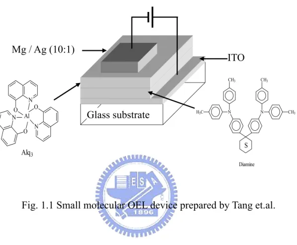
Fig. 1.1 Small molecular OEL device prepared by Tang et.al.………… 2
Fig. 1.2 Structures of some common small molecules……… 3
Fig. 1.3 Structures of some common polymer materials……… 4
Fig. 1.4 Structure of a multilayer device……… 5
Fig. 1.5 激發分子的釋能機制……… 7
Fig. 1.6 The structure of Iridium complex materials……… 9
Fig. 1.7 The synthetic route of precursor approach in PPV……… 11
Fig. 1.8 The structure of PPV derivates……… 11
Fig. 1.9 Polymer structures (a)unsubstituted PPP(b)substituted PPP(c)C9 position substituted Polyfluorene……… 12
Fig. 1.10 The fluorene based copolymers……… 13
Fig. 1.11 材料的維度(dimension):(a)零維、(b)一維、(c)二維 奈米材 料……… 15
Fig. 1.12 電子與電洞在奈米材料內形成自組的穩定態……… 16
Fig. 1.13 金屬與半導體之塊材及奈米材料的能帶結構圖……… 17
Fig. 1.14 Structures of sisesquioxanes……… 20
Fig. 1.15 The structure of T8……… 21
Fig. 1.16 半導體奈米材料的尺寸與發光波長變化圖。由左而右分別代 表InAs、InP、CdSe 奈米晶粒,尺寸愈小發光波長愈短。…… 27
Fig. 4.1 Synthesis of dimmer……… 57
Fig. 4.2 The mechanism of hydrosilylation(Chalk-Harrod’s) ………… 58
Fig. 4.3 FT-IR spectra of POSS-SiH,C-1 and POSS1……… 59
Fig. 4.4 FT-IR spectra of POSS-SiH,C-2 and POSS2……… 60
Fig. 4.5 FT-IR spectra of POSS-SiH,C-3 and POSS3……… 60
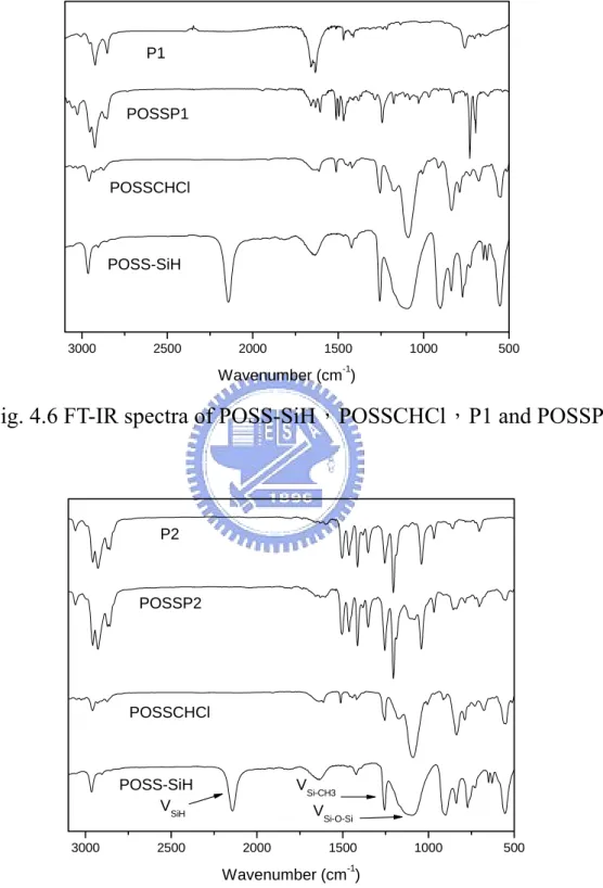
Fig. 4.6 FT-IR spectra of POSS-SiH,POSSCHCl,P1 and POSSP1…… 61
Fig. 4.7 FT-IR spectra of POSS-SiH,POSSCHCl,P2 and POSSP2…… 61
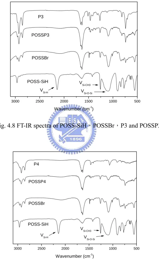
Fig. 4.8 FT-IR spectra of POSS-SiH,POSSBr,P3 and POSSP3…… 62
Fig. 4.9 FT-IR spectra of POSS-SiH,POSSBr,P4 and POSSP4…… 62
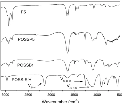
Fig. 4.10 FT-IR spectra of POSS-SiH,POSSBr,P5 and POSSP5…… 63
Fig. 4.11 UV and PL of C-1 in different solution and film states……… 69
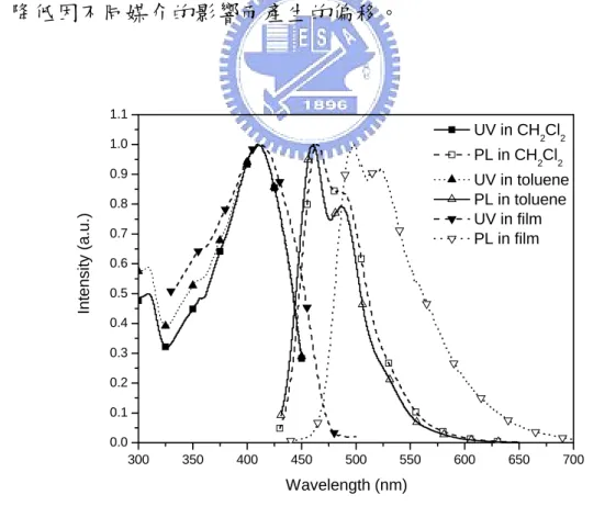
Fig. 4.12 UV and PL of POSS1 in different solution and film states…… 70
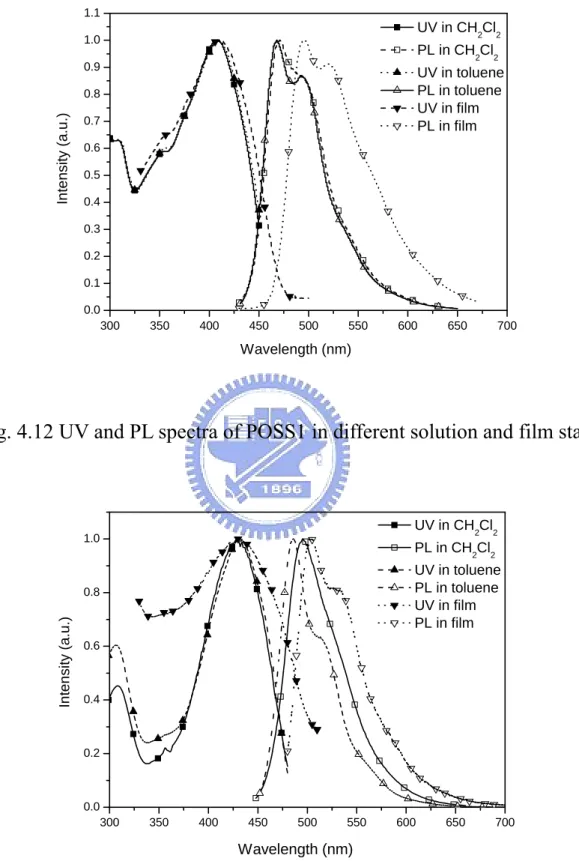
Fig. 4.13 UV and PL of C-2 in different solution and film states……… 70
Fig. 4.14 UV and PL of POSS2 in different solution and film states…… 71
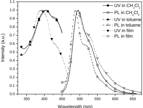
Fig. 4.15 UV and PL of C-3 in different solution and film states……… 71
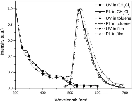
Fig. 4.17 UV and PL of P1 in different solution and film states………… 72
Fig. 4.18 UV and PL of POSSP1 in different solution and film states… 73
Fig. 4.19 UV and PL of P2 in different solution and film states………… 73
Fig. 4.20 UV and PL of POSSP2 in different solution and film states… 74
Fig. 4.21 UV and PL of P3 in different solution and film states………… 74
Fig. 4.22 UV and PL of POSSP3 in different solution and film states… 75
Fig. 4.23 UV and PL of P4 in different solution and film states………… 75
Fig. 4.24 UV and PL of POSSP4 in different solution and film states… 76
Fig. 4.25 UV and PL of P5 in different solution and film states………… 76
Fig. 4.26 UV and PL of POSSP5 in different solution and film states… 77
Fig. 4.27 SEM figure of POSS 1……… 77
Fig. 4.28 SEM figure of POSS 2……… 78
Fig. 4.29 SEM figure of POSS 3……… 78
Fig. 4.30 PL spectra of P1 and POSSP1 under different concentration… 80
Fig. 4.31 PL spectra of P2 and POSSP2 under different concentration… 80
Fig. 4.32 PL spectra of P3 and POSSP3 under different concentration… 81
Fig. 4.33 PL spectra of P4 and POSSP4 under different concentration… 81
Fig. 4.34 PL spectra of P1 and POSSP5 under different concentration… 82
Fig. 4.35 Normalized UV-Vis absorption and photoluminescence (PL)
spectra of C1 and POSS1 spin-coated film after the following treatment: (a) fresh film and annealed at (b)100 (c)150 (d)200 °C for 1h each……… 85
Fig. 4.36 Normalized UV-Vis absorption and photoluminescence (PL)
spectra of C2 and POSS2 spin-coated film after the following treatment: (a) fresh film and annealed at (b)100 (c)150 (d)200 °C for 1h each……… 86
Fig. 4.37 Normalized UV-Vis absorption and photoluminescence (PL)
spectra of C3 and POSS3 spin-coated film after the following treatment: (a) fresh film and annealed at (b)100 (c)150 (d)200 °C for 1h each……… 87
Fig. 4.38 Normalized UV-Vis absorption and photoluminescence (PL)
spectra of P1 and POSSP1 spin-coated film after the following treatment: (a) fresh film and annealed at (b)100 (c)150 (d)200 °C for 1h each……… 88
Fig. 4.39 Normalized UV-Vis absorption and photoluminescence (PL)
spectra of P2 and POSSP2 spin-coated film after the following treatment: (a) fresh film and annealed at (b)100 (c)150 (d)200 °C for 1h each……… 89
Fig. 4.40 Normalized UV-Vis absorption and photoluminescence (PL) spectra of P3 and POSSP3 spin-coated film after the following treatment: (a) fresh film and annealed at (b)100 (c)150 (d)200
°C for 1h each……… 90
Fig. 4.41 Normalized UV-Vis absorption and photoluminescence (PL) spectra of P4 and POSSP4 spin-coated film after the following treatment: (a) fresh film and annealed at (b)100 (c)150 (d)200 °C for 1h each……… 91
Fig. 4.42 Normalized UV-Vis absorption and photoluminescence (PL) spectra of P5 and POSSP5 spin-coated film after the following treatment: (a) fresh film and annealed at (b)100 (c)150 (d)200 °C for 1h each……… 92
Fig. 4.43 FT-IR spectra of P3 and POSSP3 film after baking at 100, 150,200°C for 1 hr. The spectra shows the magnified C=O stretching mode at 1721cm-1……… 93
Fig. 4.44 FT-IR spectra of P4 and POSSP4 film after baking at 100, 150,200°C for 1 hr. The spectra shows the magnified C=O stretching mode at 1721cm-1……… 93
Fig. 4.45 FT-IR spectra of P5 and POSSP5 film after baking at 100, 150,200°C for 1 hr. The spectra shows the magnified C=O stretching mode at 1721cm-1……… 94
Fig. 4.46 Energy level of POSS1~POSS3……… 97
Fig. 4.47 Energy level of POSSP1~POSSP5……… 97
Fig. 4.48 Cyclic voltammetry curve of C-1……… 98
Fig. 4.49 Cyclic voltammetry curve of POSS1……… 98
Fig. 4.50 Cyclic voltammetry curve of C-2……… 99
Fig. 4.51 Cyclic voltammetry curve of POSS2……… 99
Fig. 4.52 Cyclic voltammetry curve of C-3……… 100
Fig. 4.53 Cyclic voltammetry curve of POSS3……… 100
Fig. 4.54 Cyclic voltammetry curve of P1……… 101
Fig. 4.55 Cyclic voltammetry curve of POSSP1……… 101
Fig. 4.56 Cyclic voltammetry curve of P2……… 102
Fig. 4.57 Cyclic voltammetry curve of POSSP2……… 102
Fig. 4.58 Cyclic voltammetry curve of P3……… 103
Fig. 4.59 Cyclic voltammetry curve of POSSP3……… 103
Fig. 4.60 Cyclic voltammetry curve of P4……… 104
Fig. 4.61 Cyclic voltammetry curve of POSSP4……… 104
Fig. 4.62 Cyclic voltammetry curve of P5……… 105
Fig. 4.64 L-V-Yield curve for the device ITO/PEDOT/POSS1/Ca/Al… 109
Fig. 4.65 L-V-Yield curve for the device ITO/PEDOT/POSS2/Ca/Al… 110
Fig. 4.66 L-V curve for the device ITO/PEDOT/POSS1:PVK:PBD/
Ca/Al with different contents of PBD……… 110
Fig. 4.67 Yield-V curve for the device ITO/PEDOT/POSS1:PVK:PBD/ Ca/Al with different contents of PBD……… 111
Fig. 4.68 L-V curve for the device ITO/PEDOT/POSS2:PVK:PBD/ Ca/Al with different contents of PBD……… 111
Fig. 4.69 Yield-V curve for the device ITO/PEDOT/POSS2:PVK:PBD/ Ca/Al with different contents of PBD……… 112
Fig. 4.70 L-V curve for the device C-1 and POSS 1……… 112
Fig. 4.71 Yield-V curve for the device C-1 and POSS 1……… 113
Fig. 4.72 EL curve of C-1 and POSS1……… 113
Fig. 4.73 L-V curve for the device C-2 and POSS 2……… 114
Fig. 4.74 Yield-V curve for the device C-2 and POSS 2……… 114
Fig. 4.75 EL curve of C-2 and POSS2……… 115
Fig. 4.76 L-V curve for the device ITO/PEDOT/POSS3:CBP/Ca/Al with different concentration and wt%……… 118
Fig. 4.77 Yield-V curve for the device ITO/PEDOT/POSS3:CBP/Ca/Al with different concentration and wt%……… 119
Fig. 4.78 L-V curve for the device C-3 and POSS3……… 119
Fig. 4.79 Yield-V curve for the device C-3 and POSS3……… 120
Fig. 4.80 EL curves of C-3 and POSS3……… 120
Fig. 4.81 L-V curve for the device ITO/PEDOT/POSS3:CBP:TPBI/ Cathode with different cathodes……… 121
Fig. 4.82 Yield-V curve for the device ITO/PEDOT/POSS3:CBP:TPBI/ Cathode with different cathodes……… 121
Fig. 4.83 L-V curve for the device ITO/PEDOT/POSS 3:CBP:TPBI/ Cathode with different TPBI wt%……… 122
Fig. 4.84 Yield-V curve for the device ITO/PEDOT/POSS 3:CBP:TPBI/ Cathode with different TPBI wt%……… 122
Fig. 4.85 L-V curve for the devices of POSSP1 and P1……… 125
Fig. 4.86 Yield-V curve for the devices of POSSP1 and P1……… 125
Fig. 4.87 EL curves of POSSP1 and P1……… 126
Fig. 4.88 L-V curve for the devices of POSSP2 and P2……… 126
Fig. 4.89 Yield-V curve for the devices of POSSP2 and P2……… 127
Fig. 4.90 EL curves of POSSP2 and P2……… 127
Fig. 4.91 L-V curve for the devices of POSSP3 and P3……… 128
Fig. 4.93 EL curves of POSSP3 and P3……… 129
Fig. 4.94 L-V curve for the devices of POSSP4 and P4……… 129
Fig. 4.95 Yield-V curve for the devices of POSSP4 and P4……… 130
Fig. 4.96 EL curves of POSSP4 and P4……… 130
Fig. 4.97 L-V curve for the devices of POSSP5 and P5……… 131
Fig. 4.98 Yield-V curve for the devices of POSSP5 and P5……… 131
Fig. 4.99 EL curves of POSSP5 and P5……… 132
Fig. 4.100 Schematic of hexagonally packed POSS molecules……… 133
Fig. 4.101 WAXD of POSS and POSS1~POSS3……… 136
Fig. 4.102 WAXD from 5 deg to 15 deg of POSS and POSS1~POSS3… 136 Fig. 4.103 WAXD of POSS and POSSP1~POSSP5……… 137
Fig. 4.104 Life time curve of POSS1 and C1……… 138
Fig. 4.105 Life time curve of POSS2 and C2……… 138
Fig. 4.106 Life time curve of POSS3 and C3……… 139
Fig. 8.1 FT-IR spectra of S-1,Au-1 and Au-2……… 151
Fig. 8.2 TGA curve of S-1……… 152
Fig. 8.3 TGA curve of Au-1……… 153
Fig. 8.4 TGA curve of Au-2……… 153
Fig. 8.5 UV and PL spectra of S-1 in solution and film states………… 155
Fig. 8.6 UV and PL spectra of Au-1 in solution and film states……… 156
Fig. 8.7 UV and PL spectra of Au-2 in solution and film states……… 156
Fig. 8.8 Luminance decay curve of S-1, Au-1 and Au-2……… 157
Fig. 8.9 Energy level of S-1,Au-1 and Au-2……… 158
Fig. 8.10 Cyclic voltammetry curve of Au-1……… 159
Fig. 8.11 Cyclic voltammetry curve of Au-1 and S-1……… 159
Fig. 8.12 Cyclic voltammetry curve of Au-2……… 160
Fig. 8.13 Cyclic voltammetry curve of Au-2 and S-1……… 160
Fig. 8.14 SEM figure of Au-2……… 161
Fig. 8.15 L-V curve for the devices C-2,C-2:Au(1:0.0625), C-2:Au(1:0.11),C-2:Au(1:0.5) ……… 165
Fig. 8.16 C-V curve for the devices C-2,C-2:Au(1:0.0625), C-2:Au(1:0.11),C-2:Au(1:0.5) ……… 165
Fig. 8.17 L-V curve for the devices of C-2,Au-1 and Au-2……… 166
Fig. 8.18 C-V curve for the devices of C-2,Au-1 and Au-2……… 166
Fig. 8.19 EL figure for the device of C-2……… 167
Fig. 8.20 EL figure for the device of Au-1……… 167
Fig. 8.22 Luminance decay curve of S-1, C2 blending with Au nanoparticle……… 168
Fig. 12.1 Gilch route 之反應機制……… 179
Fig. 12.2 直接式 ligand exchange……… 180
Fig. 12.3 間接式 ligand exchange……… 180
Fig. 12.4 Mechanism of Gilch polymerization, and potential side
reaction resulting in TBB……… 181
Fig. 12.5 FT-IR spectra of S1PPV and S1PPV-CdSe……… 182
Fig. 12.6 FT-IR spectra of S2PPV and S2PPV-CdSe……… 183
Fig. 12.7 FT-IR spectra of S3PPV and S3PPV-CdSe……… 183
Fig. 12.8 Polymer distribution curve of S1PPV and S1PPV-CdSe……… 184
Fig. 12.9 Polymer distribution curve of S2PPV and S2PPV-CdSe……… 185
Fig. 12.10 Polymer distribution curve of S3PPV and S3PPV-CdSe……… 185
Fig. 12.11 TEM image of CdSe/ZnS……… 186
Fig. 12.12 TEM image of S1PPV-CdSe……… 187
Fig. 12.13 TEM image of S2PPV-CdSe……… 187
Fig. 12.14 TEM image of S3PPV-CdSe……… 188
Fig. 12.15 TGA curve of S1PPV and S1PPV-CdSe……… 189
Fig. 12.16 TGA curve of S2PPV and S2PPV-CdSe……… 189
Fig. 12.17 TGA curve of S3PPV and S3PPV-CdSe……… 190
Fig. 12.18 UV and PL of S1PPV in different solution and film states…… 193
Fig. 12.19 UV and PL of S1PPV-CdSe in different solution and film
states……… 193
Fig. 12.20 UV and PL of S2PPV in different solution and film states…… 194
Fig. 12.21 UV and PL of S2PPV-CdSe in different solution and film
states……… 194
Fig. 12.22 UV and PL of S3PPV in different solution and film states…… 195
Fig. 12.23 UV and PL of S3PPV-CdSe in different solution and film
states……… 195
Fig. 12.24 UV and PL spectra of S3PPV-CdSe in solution……… 196
Fig. 12.25 Energy level of S1PPV-CdSe~S3PPV-CdSe……… 197
Fig. 12.26 Cyclic voltammetry curve of S1PPV……… 198
Fig. 12.27 Cyclic voltammetry curve of S1PPV-CdSe……… 198
Fig. 12.28 Cyclic voltammetry curve of S2PPV……… 199
Fig. 12.29 Cyclic voltammetry curve of S2PPV-CdSe……… 199
Fig. 12.30 Cyclic voltammetry curve of S3PPV……… 200
Fig. 12.31 Cyclic voltammetry curve of S3PPV-CdSe……… 200
Fig. 12.32 C-V curve for the devices of S1PPV,S1PPV/CdSe and
Fig. 12.33 L-V curve for the devices of S1PPV,S1PPV/CdSe and S1PPV-CdSe……… 204
Fig. 12.34 Yield-V curve for the devices of S1PPV,S1PPV/CdSe and
S1PPV-CdSe……… 204
Fig. 12.35 EL curve for the devices of S1PPV-CdSe……… 205
Fig. 12.36 C-V curve for the devices of S2PPV,S2PPV/CdSe and
S2PPV-CdSe……… 205
Fig. 12.37 L-V curve for the devices of S2PPV,S2PPV/CdSe and
S2PPV-CdSe……… 206
Fig. 12.38 Yield-V curve for the devices of S2PPV,S2PPV/CdSe and
S2PPV-CdSe……… 206
Fig. 12.39 EL curve for the devices of S2PPV-CdSe……… 207
Fig. 12.40 C-V curve for the devices of S3PPV,S3PPV/CdSe and
S3PPV-CdSe……… 207
Fig. 12.41 L-V curve for the devices of S3PPV,S3PPV/CdSe and
S3PPV-CdSe……… 208
Fig. 12.42 Yield-V curve for the devices of S3PPV,S3PPV/CdSe and
S3PPV-CdSe……… 208
Fig. 12.43 EL curve for the devices of S3PPV-CdSe……… 209
Fig. 12.44 logμ-E curve for the hole only devices of S1PPV~S3PPV and
S1PPV-CdSe~S3PPV-CdSe……… 210
Fig. 12.45 logμ-E curve for the electron only devices of S1PPV~S3PPV
and S1PPV-CdSe~S3PPV-CdSe……… 211
Fig. 12.46 logμ-E curve for the hole only and electron only devices of
第一章 緒論
1.1 有機電激發光元件與基本原理簡介
有機電激發光(Organic Electroluminescence, OEL)的研究肇始於 1950 年早期,Bernanose 等人於 1953 年對分佈於高分子中的有機染料(Acridine
或 Quinacrin)施以交流電壓觀察到了發光現象[1],當時他們解釋此發光原
理 應 類 似 於 傳 統 III-V 族 元 素 所 組 合 的 薄 膜 式 電 激 發 光 板 ( thin-film
electroluminescence panel, TFEL),如 ZnS。其後於 1963 年 Pope 等人於 Anthracene 晶體兩端跨接 400 伏以上之高電壓,觀察到發光現象,不過其發
光強度仍低[2];至 1965 年,Helfrich 和 Schneider 利用含有 AlCl3-anthracene
(陰極)和Na-anthracene(陽極)的電解質溶液成功的製備出高亮度的 EL
元件[3,4] ,並成為第一篇有機電激發光的專利文獻。但事實上單晶體的有機
材料是無法用來製作優良的EL 元件,所以其後的二十年間雖然有人陸續利
用 Anthracene 單晶製作元件,並繼續從事相關發光機制、電荷轉移、注入
電流及量子效率(Quantum Efficiency)的研究,但距離實用階段仍有很大
的差距。直至1987 年美國 Eastman Kodak 公司的 Tang 和 Van Slyke 等人利
用真空蒸鍍非晶系(amorphous)有機薄膜的技術以及創新的異質介面
(heterojunction)多層有機薄膜之元件結構[5],如 Fig.1.1 所示。Indium-tin
oxide(ITO)及鎂銀合金(Mg-Ag alloy)分別當作陽極及陰極,Aromatic diamine 作為電洞傳輸層(Hole Transport Layer),Tris(8-hydroxyquinoline)
aluminum (III)(Alq3)當作發光層(Emission Layer),發表了第一個高亮度
的薄膜有機 EL 元件,他們大幅地改善了有機電激發光元件的特性(<10V
的操作電壓,> 1%,的量子效率)及穩定性,成為第一個接近實用的小分
子真空蒸鍍OEL 元件,也因此激起了世人對 OEL 的興趣,並廣泛積極地投
入研究。該元件的特徵是採用具有孤電子對(Electron lone pair)的芳香烷 胺類(Aromatic diamine)做為電洞傳輸層,增加電洞的傳輸效果,另採用
能吸引電子的鋁錯體(Alq3)做為電子傳輸層(Electron Transport Layer)兼
幅提昇,而且有機層膜厚只有 1000Å,才得以實現以 10V 低電壓驅動,得
到1000 cd/m2以上的劃時代亮度。
Fig. 1.1 Small molecular OEL device prepared by Tang et.al.
從Pope 等人至柯達公司所用的材料仍以有機小分子為主,利用分子上
的設計,於適當位置導入推電子基或拉電子基,藉此調整其共軛長度,使 光色可達到紅、綠、藍之三原色光,並利用陣列化之技術,可製作出全彩
化之顯示器,見Fig. 1.2。如 Alq3為常用之綠光材料,B-Alq3為藍光材料,
而DCJTB 則為紅光材料。而在電洞傳輸層上,則以發展具有高玻璃轉移溫 度(Tg)之芳香烷胺類為主。利用其星狀結構,增加其熱穩定性及避免結晶的 產生。並且在某些元件上,由於發光層本身傳輸電子效率並不良好,為平 衡電洞及電子,增加其結合效率,會於發光層上蒸鍍一層電子傳輸層,以 增進其元件之表現。 Glass substrate Mg / Ag (10:1) N O N O N O Al Alq3 N N H3C CH3 CH3 CH3 Diamine S ITO
Fig. 1.2 Structures of some common small molecules. [6~9] N N NPB N N N N MTDATA Hole transport materials
N N O t-PBD N N N N N N TPBI Electron transport materials
N O N O Al N O N O Al N O O Alq3 B-Alq3 O NC CN N DCJTB DPVBi
在有機高分子OEL 元件的發展方面,1982 年 Patridge 等人利用旋轉塗
佈方式(Spin-coating)製作出第一個高分子的 OEL 元件[10],當時所利用的
材料是poly(vinylcarbazole)(PVK)。但真正讓有機高分子用於 OEL 受到重
視的則是1990 年英國劍橋大學卡文迪西實驗室(Calvendish Lab.)所發表,
利用poly(p-phenylene vinylene)(PPV)所製造的 OEL 元件[11]。他們利用前
驅物法(Precursor route)將高分子前驅物塗佈於導電玻璃表面,再經過熱 脫去反應製成了共軛聚合物,並鍍上鋁金屬做為陰極,製做出第一個以共
軛高分子為發光材料的OEL 元件,引發了第二波的 OEL 元件的研究熱潮。
劍橋大學更於1992 年成立 Cambridge Display Technology(CDT)公司,致
力於發展高分子 OEL 材料與元件技術。自此 Kodak 與 CDT 各自成為發展
小分子與高分子 OEL 研究的兩大巨擘。常見的 OEL 高分子材料結構如
Fig.1.3 所示。
Fig. 1.3 Structures of some common polymer materials.
OEL 元件本質上為一固態半導體元件,其所使用的材料是有機半導體 而非傳統的無機半導體。傳統發光二極體是利用無機材料III-V A 族或 II-VI A 族化合物半導體所製成,以原子為基本單位;而大部分的有機半導體則 是由所謂的“共軛分子"或“共軛高分子"所構成,由於分子間的交互作 用遠較原子間之交互作用為弱,因此有機半導體通常帶著強烈的分子本身 S R N CH2 CH R R PPP PPV PT PVK PF n n n n n
的色彩。共軛高分子在聚合物主鏈上含有大量的π電子,在主鏈中形成不 定形位移(Delocalization),此不定形位移被認為是影響共軛高分子能階差 (Band-gap)之主要因素,也進而影響其光電性質。在共軛高分子中又以 PPV,見於 Fig.1.3。系統最常做為有機發光二極體的發光材料,將 PPV 薄 膜夾於上金屬陰極和下金屬陽極之間,整個元件製作在透明基板如玻璃或 PET(塑膠基板)[12]上,透明陽極通常是由 ITO(摻雜錫(Tin)之氧化銦
(Indium Oxide))所構成,陰極則選用功函數(Work function)較小的金屬 如鈣或鋁,當一順向偏壓加諸於陽極和陰極之間時,電洞和電子分別自陽 極和陰極注入有機半導體,二者在有機薄膜中傳導而相遇,經由載子的再 結合(Recombination)伴隨輻射性衰變(Radiative decay)的方式而產生光 子(photon),透過透明基板而發光。為了增加電荷注入與傳輸以增進發光 效率,亦可以於發光層和陽極間加入電洞傳輸層,於發光層和陰極間加入 電子傳輸層,成形成多層結構的有機發光元件,如Fig.1.4 所示。
Fig. 1.4 Structure of a multilayer device
1.2 有機電激發光機制
激發至激發態(excited state)的能階,此時位於激發態的電子即稱為激子 (exciton)。激子隨即會以不同的能量方式(光或熱)衰退返回基態,其間的能 量差值,將視材料分子的化學結構。一般的非共軛性材料大部份是以熱的 形式放出;而共軛性結構之材料,則會有若干比例以光的形式釋出。 當電子被激發後,由基態躍遷至激發態,受到激發的電子將依不同的 途徑釋出能量回到基態,其過程說明如下[13]:
(1) 振動鬆弛(vibrational energy relaxation):
分子被激發至電子激發能(S1)的某一振動激發態上,緊接著由於分子間 或與溶劑分子的相互碰撞而以熱的方式耗散其部份能量,從振動激發態鬆 弛到 S1的最低振動態上,此一過程即為振動鬆弛。振動鬆弛發生的時間大 約在10-14~10-12s 的量級,小於螢光輻射躍遷的壽命(10-8),所以螢光輻射躍 遷的始態幾乎都是S1 的最低振動態。 (2) 內轉換(internal conversion,IC) 激發態分子經過非輻射躍遷耗散能量而落回相同自旋度低能態的過程 稱之為內轉換。與振動鬆弛不同的是,其為一種”能態間”的過程。內轉換發 生的速率為 10-12s 左右,由於它的存在,我們很難觀察到由 S2以上的激發 單重態至基態的螢光輻射躍遷,絕大多數的螢光躍遷是 S1ÆS0。此外,螢 光和內轉換是相互競爭的,一個分子的螢光性能好壞,不但決定於螢光發 射速率常數(kf),還受到內轉換速率常數(kic)所控制。 (3) 外轉換(external conversion) 指激發分子會因與未激發分子或溶劑分子等其它分子間相互作用而進 行能量轉移,此時能量轉移以熱或其他型式釋出。 (4) 系統間跨越(intersystem crossing,ISC) 若S1與T1能階交疊或有很好的耦合,電子則可能改變其自旋方向進入 T1,此過程即為系統間跨越。於 T1的電子以輻射方式回到基態的過程即為 磷光(phosphorescence)。如果兩能階的耦合較小,則大部份激發分子仍將在 S1態內鬆弛,最終以螢光(fluorescence)或內轉換的方式回至基態。
Fig. 1.5 激發分子的釋能機制
1.3 對苯二乙烯衍生物於光化學上的應用
[14] 開發合成新的 OPV(oligo(phenylenevinylene))衍生物一直以來都受到相 當大的注意[15],因為其具有廣泛的應用性,如電激發光二極體、化學感應 器、非線性光學材料和有機電磁性材料等。由於 HOMO 和 LUMO 能階差 的不同,而決定了這些材料的不同應用性。 增加苯乙烯鏈的長度可以減少 HOMO 和 LUMO 的能階差,可以藉此 調整光色。然而苯乙烯鏈到了一定長度後[16](10 單位的苯基和九個雙鍵), 由於電子分散程度達到一定飽和極限,使得螢光光譜不會持續地紅移而只 能到536nm 。 共軛雙鍵系統下的分子中,D-A-D 的分子會比 D-π-D 分子有更強的紅位移現象,這是因為電荷轉移(charge transfer)的運動中,外部的推電子基在 中間有拉電子基時,其共振運動更容易產生。 此外,OPV 的架構上,可以於外圍兩端接上不同基團以改變其共軛長 度及光電性質。最常見的是引入苯胺基團,除了做為電洞傳輸的成份外, 也可以加強螢光的延緩(fluorescence decay)[17]。
1.4 磷光元件之發展
由於自旋禁阻(spin forbidden)的限制,螢光電激發光元件的激發三重態 都 以 非 輻 射 的 方 式 表 現 , 所 以 元 件 的 內 部 量 子 效 率 理 論 上 最 大 值 為 25%[18]。相較之下,有機磷光發光材料理論上可使內部量子效率提高至接 近100%[19]。但由於有機磷光材料在室溫下發射效率不高,三重態生命期過 長,限制了元件的使用性,且高濃度時會有濃度驟熄(concentration quenching) 的現象。在1998 年,美國普林斯頓大學(Princeton) Forrest 小組於「Nature」[20]
所發表的成果指出,將高效率的磷光材料(PtOEP)摻雜在主體材料中,能量
從主體傳遞到磷光材料中發光,可以將外部量子效率提高到4%,從此開啟
了磷光發光材料的熱潮。具有高效率的磷光摻雜物(dopant)多是含重原子的 材料,這是由於重原子可使得電子自旋-軌道耦合(spin-orbital coupling)作用
增強,有效地混合單重態與三重態,增加 S1ÆT1系統間穿越的機率,此現
象即為”重原子效應(heavy atom effect)”。除此之外,重原子的加入也可以減 低三重態的放光生命期。
料。由於其較 PtOEP 具有更短的三重態生命期,可以減少在高電流密度下 的磷光飽和(saturation),避免三重態-三重態的驟熄(T-T annihilation),因此 可提高元件於高電流密度下的外部量子效率。並且利用選則不同之芽基
(ligand),可發射出紅、綠、藍三原色光[21~23],如 Fig. 1.6 中所示。
Fig. 1.6 The structure of Iridium complex materials
磷光有機電激發光元件的結構包括電洞傳輸層、摻雜磷光材料的發光 層、抑止激發子擴散的電洞阻擋層和電子傳輸層(HTL/EML/HBL/ETL)。由 於磷光的三重激發態生命期很長,三重態激子的擴散範圍較單重態電子大 上許多,為了提高元件效率,必須將三重態激子限制在發光層中,如此才 能有效地將能量從主體傳遞到客體,因此需要有電洞阻擋層(hole blocking layer,HBL)的存在[24]。作為 HBL 的材料具有極大的游離能,可以阻擋激 子的擴散,尤其當主體與客體軌道重疊弱時,此層的功用更是重要。 磷光材料結構大多由過渡金屬及配位基組成,此類過渡金屬錯合物常 見的有三價銥錯合物和二價鉑錯合物。之所以選用此類過渡金屬錯合物是 因為這些金屬擁有d6電子組態、具較強的鍵結、long-lived 激發態和較高發 光效率等特性[25],得以加強發光強度和減少非輻射衰退。對於原子序 O O N Ir 2 O O N Ir F F 2 2 O O N Ir S 2 O O N Ir S
Ir(ppy)2(acac) (green)
Ir(btp)2(acac) (red) Ir(thp)2(acac) (green) Ir(Fppy)
2(acac) (blue) 2 Irppy3 (green) N N Ir O N N Ir F F O 2 Firpic
Z=75~77 的重金屬離子而言,因為擁有較強的自旋軌域耦合(spin-orbit coupling),增加系統間跨越能力,使得單重態激發態跳躍至三重態激發態的 機率增高,進而增加磷光放光效率。 有機磷光材料由於可以善用激發三重態的能量,使得有機電激發光元 件的外部量子效率得以有效提升,但是仍有幾點需要特別留意的。首先, 室溫下的磷光材料較少,所以材料的選擇範圍較螢光材料少;再者,磷光 材料由於激發態的生命期長,於高電流密度下易有三重態-三重態的驟熄 (T-T annihilation)的現象產生,使得元件效率下降;最後,值得注意的是環 境中氧對三重態有驟熄的影響,這是因為基態氧也是三重態,它對激發三 重態有強烈的驟熄能力,不加以保護就會影響元件的發光強度及壽命。
1.5 聚對苯乙烯(poly(p-phenvylene vinylene))於發光元件
上之應用
近十年來,高分子有機發光二極體在材料的研發上有相當多的研究, 其中PPV由於成膜性佳及具有高螢光的特性,因此目前有相當多以PPV作為 發光層的文獻報導。PPV 能階差( bandgap )大約是2.5 eV,最大放射波長 為551 nm和520 nm,是屬於一個黃綠光的螢光材料。由於其為一不可溶之 材料,故一般製備方法為使用前驅物法[26]。其方式為先將可溶性的前驅物 高分子(precursor polymer) 旋轉塗佈於基材上,再進行加熱脫去反應而形成 所需的共軛高分子,如Fig. 1.7所示。為增加其應用性,Wudl等人首先以Gilch route[27]合成雙邊烷氧基團取代之MEH-PPV[28],此類聚合物可溶於
一般有機溶劑,大量的簡化其製程步驟。其電激發光最長波長為 610nm, 為橘紅光,能隙為2.1eV,量子效率可達2%。原因是因為MEH-PPV 側鏈烷 氧基上的氧原子上孤對電子具推電子效應,可以使其主鏈上共軛性增加, 導致PPV 高分子共軛主鏈上的電子密度增加,即可增加PPV高分子主鏈上 共軛系統之電子共軛性,而降低PPV之最高階填滿分子軌域(HOMO)與最低 階未填滿分子軌域(LUMO)之間能隙,使發光波長紅位移至橘紅光到紅光波 長範圍[29]。
Fig. 1.7 The synthetic route of precursor approach in PPV
在之後之十幾年,大量的研究利用取代基之改變或共聚合之方式來改
變光色,可使PPV高分子之光色由藍到紅[30~32]。亦有研究利用導入傳導電洞
或電子之基團,來得到高效率之有機發光元件[33,34]。如Fig. 1.8所示。
Fig. 1.8 The structure of PPV derivates
ClH2C CH2Cl Cl Cl S S n a b, c, d e Cl S 1 o a) tetrahydrothiophene , MeOH, 65
b) NaOH, MeOH/H2O or Bu4NOH, NaOH, 0 C
c) neutralization(HCl) d) dialysis(water) e) 180 - 300 C , vacuum, 12 Hr o C o C10H21 N N O O C8H17 Si Si O O O O C8H17 C8H17 NC CN O O C8H17 n n n n n n DP10-PPV (blue-green) MEH-PPV (orange-red) O C8H17 N o-PBTMSPPV (blue) CN-PPV (Red) Carbazole-PPV (green) Oxadiazole-PPV (green)
1.6 聚芴(polyfluorene)於發光元件上之應用
早期Poly(p-phenylene) (PPP)如 Fig. 1.9(a)所示,因為它有較大的能階差
符合產生藍光的需求而被發展,PPP 是以苯環為重複單位( reapting unit )所 構成的高分子,然而一旦形成高分子後則無法溶解於有機溶劑裡,故在加 工處理上極其不便,之後為了使 PPP 能溶在有機溶劑裡,便在苯環上導入 取代基團以增加聚合之後的溶解度,如Fig. 1.9(b)所示,取代基團的導入確 實大大提高其在有機溶劑中的溶解度,但也因為取代基團的介入使的 PPP 的共軛主鏈受到嚴重的扭曲,而使得在苯環間的共軛程度大大的降低致使 發光效率不佳,爾後,便有Ployfluorene 的發光材料被發展出來。
Fig. 1.9 Polymer structures (a) unsubstituted PPP (b) substituted PPP (c) C9 position substituted Polyfluorene
Polyfluorene 的結構類似 PPP,其結構包含了剛硬的雙苯環(biphenyl)單 位,它導致了一個較大的能階差而可有效率發出藍光,而且在遠離共軛主 鏈的C9 碳上接上柔軟的取代基團,則可提供改進高分子的溶解度及加工性 的機會,但卻不會使共軛主鏈產生明顯扭曲而導致共軛程度不佳的缺點[35]。 poly(2,7-(9,9-diaklyfluorene))雖然此材料的能階差夠大,足以形成藍光 且效率上也較一般藍光材料佳,但其熱穩定度( thermal stability )卻較差,主 要原因為其玻璃轉移溫度(Tg)並不高,故當元件通電後致使溫度不斷升高, 最後超越其玻璃轉移溫度時,其高分子鏈結構便往具備最低能量的構形 ( conformation )轉換,使共軛面與共軛面平行排列,這時便易產生 excimer emission[36],致使元件所發出的光色產生改變。 為了改善這個問題專家學者便開始設計出具有較高玻璃轉移溫度的分子 R R n R R n n
(a)
(b)
(c)
結構出來[37~39],其結構如下所示: 以上高分子本身結構已具備高玻璃轉移溫度的特質,故能減緩因元件 溫度上升所造成的堆疊效應(aggregation)。 以 fluorene 為單體的高分子,其元件的效率表現佳,藉由共聚合的方 式,可改變其光色由藍變紅,亦可導入傳導電洞或電子之基團,來得到高 效率之有機發光元件[40~45]。如Fig. 1.10 所示。
Fig. 1.10 The fluorene based copolymers
OC8H17 H17C8O H17C8O Ph Ph Ph Ph Ph Ph Ph Ph n n n N N NC CN H17C8 C8H17 n H17C8 C8H17 N C4H9 n H17C8 C8H17 N C4H9 N C4H9 n H17C8 C8H17 N S N n H17C8 C8H17 n H17C8 C8H17 S S O O C8H17 NC CN n Blue Blue Green Green Red Red
1.7 奈米材料之簡介
由於近年來高科技產業對微小化材料之需求日漸增加,使得奈米材料 之發展成為全球高科技國家之重點項目,舉凡光、電、磁[46]、機械、催化[47] 等領域都需要材料之奈米化以得到更大的提升。所謂的奈米(Nanometer), 所表示的為億分之一米,為介於原子、分子與巨觀尺度之間,一般定義為 直徑小於 100nm 的粒子。而所謂的奈米科技,就是將各式元件之基本構造 縮小至奈米的程度。事實上,奈米不過是一很小的尺寸單位,為何會受到 大家如此之重視呢?其主要原因是由於當物質小於奈米尺度時,相對於塊 材而言,由於量子效應、物質之局限性以及巨大的表面和界面效應,可使 得其物理特性及化學特性產生奇特之變化。包括高延展性、高硬度、低熔 點以及不同於塊材之導熱性、導電性、催化性[48]、磁性及光學性質[49,50]等 都會產生質的變化[51,52]。而奈米技術即利用這些特性,廣泛的應用於光電 [53,54]、資訊、生醫[55~58]等產業上。 奈米材料可以簡單的由其外觀的幾何結構分為下列三種,如 Fig. 1.11 所示: 一、零維(zero-dimensional)的奈米結構: 零 維 的 奈 米 結 構 稱 為 奈 米 粒 子(nanoparticles) 或 是 量 子 點 (quantum dots),其結構是在三維空間中之 X 軸、Y 軸與 Z 軸均極微小(小於 100nm), 如Fig. 1.11 (a) 所示。 二、一維(one-dimensional)的奈米結構: 一維的奈米結構若縱深比(aspect ratio)較大者稱為奈米線(nanowires), 較小者稱為奈米棒(nanorods),其結構是在三維空間中的 X 軸可以無限延 伸,但是Y 軸與 Z 軸均極微小(小於 100nm),如 Fig. 1.11 (b) 所示。 三、二維(two-dimensional)的奈米結構: 二維的奈米結構稱為奈米薄膜(nanofilm)或量子井(quantum well),其結 構是在三維空間中的 X 軸與 Y 軸可以無限延伸,但是 Z 軸極微小(小於 100nm),如 Fig. 1.11 (c) 所示。(a) (b) (c)
Fig. 1.11 材料的維度(dimension):(a)零維、(b)一維、(c)二維奈米材料
而奈米材料所表現出之特性最主要有以下兩種,
一、量子局限效應(Quantum confinement effect)[59]
材料的物理性質大部分是由電子與電洞所決定,例如Debye長度用來描 述材料中電子與電子之間作用力的長度、de Broglie波長用來定義材料的粒 子性質與波動性質[60],由於傳統三維空間的塊材(bulk)尺寸遠大於上述這些 電子與電洞的物理特徵長度,因此其物理性質可以使用古典物理來解釋, 但是當材料的尺寸小到100nm 以下時,與這些特徵長度相近,因此會產生 許多特別的現象。當材料的尺寸小於電子或電洞的波包尺寸時會產生量子 局限效應,此時電子與電洞被局限在奈米材料內形成自組的穩定態,如Fig. 1.12 所示[61],圖中電子的波函數受到奈米晶粒內與晶粒外的能階影響,使
得電子被局限在奈米晶粒之內,在這樣的情況下,傳統三維空間的塊材中 連續的能帶消失,而產生離散的能階[62],如Fig. 1.13所示,圖中可以看出半 導體塊材的價電帶與導電帶是連續的能帶,而奈米晶粒則會形成離散的能 階,這種現象會造成發光性質的改變[51]。以半導體粒子中所表現出之量子 局 限 現 象 為 例 , 半 導 體 材 料 可 以 分 為 元 素 半 導 體 以 及 化 合 物 半 導 體 (compound semiconductor),元素半導體主要以我們熟知的矽與鍺為主;化 合物半導體有兩種主要的形式:III V 族半導體,如: GaN、GaAs、lnP 和II VI 族半導體,如: CdSe、CdTe。研究發現當半導體粒子的粒徑減少時,價 帶與傳導帶之間的能隙(energy gap)會跟著增加。當CdSe 奈米粒子的價 電子經由照光的方式激發到傳導帶之後,會自發性的將能量釋放而回到價 帶。相對地,若有不同大小的CdSe奈米粒子經由同樣的激發光源照光時, 由於量子侷限效應,他們有著不同的能隙,所以減少粒子的粒徑會放出較 短波長的光並會有藍位移的現象[62~65]。 Fig. 1.12 電子與電洞在奈米材料內形成自組的穩定態
Fig. 1.13 金屬與半導體之塊材及奈米材料的能帶結構圖
二、表面與界面效應(Surface and interface effect)
隨著顆粒直徑的減少,比表面積將會顯著的增大,表面原子佔總原子 數的百分比也將迅速增加。假如以球形的奈米粒子為例,若是其半徑為r, 所含的原子總數為n,那麼不同大小的一個球形金粒子裡頭的總原子數與表 面原子的比例如Table 1.1所示[66],其計算方式如下: S = 4p.ro2.n2/3,其中ro 為其組成單元原子的半徑,S 代表奈米粒子的 表面積 (nm)。 表面原子數可以表示為ns = 4n2/3 表面原子數占總原子數的比例(K)為K = 4/n1/3
Table 1.1 奈米粒子中所含的原子數以及表面原子所佔的比例(%) 由此可見,當粒子直徑由10 nm 到5 nm 時,表面的原子數比例從20% 提高到40%;到1 nm 時,表面原子數比例更是提高到99%。因此,當顆粒 的直徑減少時,會引起他的表面原子數、表面積和表面活性的大幅增加。 同時,表面原子具有高的表面能,且不穩定,他很容易與外來的原子吸附 鍵結,形成穩定的結構。因此,表面原子與內部原子相比,具有更大的化 學活性和提供大面積的表面活性原子。對外界環境如溫度、光、濕度、氣 體等十分敏感,對於環境些微的改變,能迅速引起材料表面離子的價電子 態和電子傳輸明顯的變化。例如光的吸收明顯增加使得金奈米粒子呈現黑 色,二氧化鈦奈米粒子(光觸媒)的表面光化學反應分解有機物質[67]等。
1.8 奈米材料在有機發光二極體元件上的應用
奈米材料應用在有機發光二極體元件上的例子並不多見,最早見於 Colvin 於 1994 年將 CdSe 混入 PPV 中,可藉由能量轉移的方式得到發 CdSe的光之元件[68]。Onitsuka 亦將 CdSe 混入 PVK 中,製作出含奈米粒子之有
機發光二極體元件,但驅動電壓過高及光色隨電壓改變為其缺點[69]。Heegar
於 1995 年將 C60混入 MEH-PPV 中,並隨著混入比例的增加,能提升其光
樣得到光伏打元件效率增加之結論[71]。而在 1997 年,Carter 利用奈米化之
TiO2及 SiO2混入 MEH-PPV 中,成功的將奈米粒子和有機發光二極體結合
在一起[72],並得到亮度及效率皆有所提升之結果,且其無驅動電壓變高及 光色隨電壓改變之缺點。但奈米粒子在有機發光二極體元件中所扮演之角 色及功能,至目前為止並無較明確之結論。有研究指出奈米粒子在元件中 能增進其電子或電洞之注入[72],亦有文獻認為奈米粒子能減緩發光分子之 光氧化反應[73,74],進而增進其效率。也因為其未知性,如何將奈米粒子和有 機發光二極體成功的結合成為一極具潛力之研究方向。
1.9 多面體矽氧烷寡聚物(POSS)材料的發展
最早在1900 年代,Kipping[75]便利用水解矽烷化合物縮合得到聚矽氧烷(Silsesquioxanes),然而一直到 1960 年時才由 Brown 與 Vogt[76,77]重新建立起
較完整的合成方法。在 1994 年美國空軍研究實驗室(US Airforce Research
Laboratory)為了發展較輕及較高性能的高分子材料,選擇了已有 30 多年發 展歷史的聚矽氧烷化合物,並投入六年的資金與人力,設計出一系列POSS 結構,並進而量產。其中,最令人印象深利的是,以POSS 改質 PMMA 使 其可以承受高溫,並利用於製造太空梭的材料上。 矽氧烷(Silsesquioxanes),其定義為一個 Si 原子接上三個 O 原子,所以 也稱T 樹脂,通常以化學式(SiO1.5)n表示。矽氧烷的結構主要為梯形(ladder)
與多面體形(polyhedron,包含 cage 和 partial cage),如 Fig. 1.14 所示[78]。多
面體矽氧烷寡聚物為單一分子結晶體,結構相當對稱,分子大小約為0.7nm
至
目前,含有六面體籠狀結構的矽氧烷(RSiO1.5)8(T8)為最廣為研究的對
象。Fig. 1.15[79]為T8的化學立體結構(籠狀,Cage-like),大小約為 1.5nm 的
六面體結晶體(rhombohedral crystal structure)[80],其由一結構剛硬的六面體
二氧化矽為中心,8 個有機取代基接在矽原子上所組成。其中的有機取代基 可分為兩大類,一為沒有反應性的有機取代基,可以增加 POSS 的溶解度; 另一為單一或多個具反應性的取代基,可以與有機分子形成共價鍵的聯 結。其中增加溶解度的基團最常見的是環戊烷基;反應性取代基則有很多 種:雙鍵、氫基、氧氫基、氯苯基等。
Fig. 1.15 The structure of T8
1.10 金奈米粒子的發展及特性
近年來,奈米金屬簇的開發與研究是相當熱門的研究課題。由於奈米
尺度(1-100 nm)下的金屬粒子具有相當特殊的電磁,光學,力學等性質[81]。
將自身組裝(self-assembly)與奈米金簇(nano gold clusters)的結合。對金屬與 介面的研究開啟了一個新的領域。早期是利用兩相系統(two-phase system)
製備膠體(colloid)的金屬粒子。Faraday[82]將水溶性的金鹽與磷酸鹽加入含有
中 。 結 合 早 期 至 被 微 小 金 顆 粒 的 兩相 合 成 分 法 與 近 年 的 離 子 萃 取(ion extraction)技術,再加上金與烷硫分子會自身吸附形成單層的特性,於1994
年,Brust發展出新的製備方式[83],以單一步驟(one step)製備奈米尺度的金
奈 米 粒 子 。 以 烷 硫 分 子 與 金 形 成 單 層 保 護 的 金 奈 米 粒 子(monolayers
protected Au clusters, MPCs)與早期的金膠體粒子的合成分具有極大的不同 點,產物的大小也有數個級數的差異。此外,亦有多種製備金奈米粒子的 方式,如雷射侵蝕法(laser ablation),氣體冷凝法(evaporation of metal in vacuum),電化學法(electrochemical method)等,但這些方法都無法達成快速 分離產物與起始物,或是避免產生奈米粒子與粒子之間團聚(aggregation)的 現象,因此可能造成分解(decomposition)的情形,此外,有些製備的方式無 法將奈米粒子溶解於一般的有機溶劑中。但是,由於這一類金屬奈米粒子 具有與傳統材料極為不同的奇異或反常的物理及化學特性,因此引發了一 股研究熱潮。 1998年,Murray等學者指出[84],可藉由AuCl4-離子與烷硫分子的比率以 及反應時的溫度和還原反應的速度控制[85]等方法調整烷硫分子形成單層保 護的金奈米粒子大小。金奈米粒子的平均大小可利用數種不同的分析儀器 加以鑑定,並且綜合這些儀器與奈米粒子的特性,可以得到具有特殊意義 的獨特光譜圖形。烷硫分子形成單層保護的金奈米粒子在1H NMR 光譜圖 中會出現line broadening 的現象[86,87]。奈米粒子大小的鑑定可利用高解析度
穿 透 式 電 子 顯 微 鏡(high resolution transmission electron microscopy,
HRTEM)[83],[84],金奈米粒子的大小是否均勻一致可使用X 光粉末繞射儀
(powder X-ray) 加 以 判 定 , 還 可 運 用 熱 重 分 析 儀 (thermo gravimetric analysis) 、 紫 外 光 譜 儀 (ultraviolet spectroscopy) 及 遠 紅 外 光 譜 儀 (Fourier transform infrared spectroscopy, FTIR)等儀器進行測量。根據小角度X 光散
射(small-angle X-ray scatting)[86]及熱重分析儀的實驗,可判定當金奈米粒子
的直徑約在1.5 ~ 5.2 nm 之間時,約含有110 ~ 4800 個金原子。而金奈米粒
子 的 電 子 性 質 可 利 用 紫 外/ 可 見 光 譜 儀[88-90] 及X-ray photoelectron