國立交通大學
電信工程學系碩士班
碩 士 論 文
應用於無線網路之低電壓(0.7V)變壓器迴授低雜訊放
大器與應用於超寬頻系統之低雜訊放大器之設計
Design of Low-voltage (0.7V) Transformer-feedback
for Wireless LAN and UWB low noise amplifier for
UWB Systems
研究生:方瑞嫻
指導教授:周復芳 博士
應用於無線網路之低電壓(0.7V)變壓器迴授低雜訊放大器
與應用於超寬頻系統之低雜訊放大器之設計
Design of Low-voltage (0.7V) Transformer-feedback for
Wireless LAN and UWB low noise amplifier for UWB
Systems
研究生:方瑞嫻
Student:Jui Hsien Fan
指導教授:周復芳 博士 Advisor:Dr. Christina F. Jou
國立交通大學
電信工程學系碩士班
碩 士 論 文
A thesis
Submitted to Department of Communication Engineering
College of Electrical and Computer Engineering
National Chiao Tung University
In Partial Fulfillment of the Requirements
For the Degree of
Master of Science
In Communication Engineering
June 2007
Hsin Chu, Taiwan, Republic of China
中 華 民 國 九 十 六 年 六 月
應用於無線網路之低電壓(0.7V)變壓器迴授低雜訊放大器
與應用於超寬頻系統之低雜訊放大器之設計
研究生
: 方瑞嫻 指導教授 : 周復芳 博士
國立交通大學電信工程學系碩士班
中文摘要
本論文的第一部份介紹低電壓低雜訊放大器電路設計方法,利用變壓器迴授來提升 輸入輸出的隔絕度取代原有的疊接的低雜訊放大器架構。實作的低雜訊放大器顯示其並 沒有達到預期的結果。第二部份探討其原因,最大的影響因素可能為晶片內部佈局不佳所 造成的。將晶片鎊線於PCB 版子上並進一步探討。 在第三部份,介紹一個寬頻的低雜訊放大器,其輸入匹配利用電晶體雜散電容來達 成 。 此 方 法 可 以 使 輸 入 匹 配 網 路 簡 化 , 並 且 減 少 雜 訊 的 貢 獻 。 其 模 擬 結 果 顯 示 3.1GHz~10.6GHz 其輸入返回損耗和輸出返回損耗皆在-10dB 以下,增益為 12dB,最小 雜訊指數為 4.5dB。但量測時與預期的模擬結果並不符合,在接下來的章節中也做了原 因探討。Design of Low-voltage (0.7V) Transformer-feedback for
Wireless LAN and UWB low noise amplifier for UWB
Systems
Student: Jui Hsien Fan Advisor: Dr. Christina F. Jou
Department of Communication Engineering
National Chiao Tung University
Abstract
In the first part of the thesis the design method of Low voltage LNA topology is studied which using transformer feedback to improve the isolation between input and output. This topology can replace the conventional LNA topology and is suited for low voltage application. The implemented LNA reveal that the unexpected measurement result. The second part of this thesis discussion the problem. The possible cause is the layout of this chip. Further, we also discussed the measurement result of chip bonded on the PCB board.
In the third part, an UWB LNA is designed. It uses the intrinsic capacitance of transistors to achieve the input matching and the complicated input matching network is replaced. The simulation result of UWB LNA demonstrates S11 < -10dB and S22 < -10dB from 3.1 to 10.6 GHz. The power gain (S21) is 12dB. The minimum noise figure is 4.5dB. The measurement result is different from the simulation result and in following section we discussed the possible problems.
Acknowledgement
首先,我要感謝指導教授周復芳老師,在這兩年來的指導和關心,讓我在碩士學業 求學過程獲益良多。同時要感謝口試委員郭建男博士及胡政吉博士的不吝指導。另外要 感謝吳匯儀學長的耐心教導,尤其當我遇到困難總能給我鼓勵和協助,並且指引了我研 究方向,讓研究更有目標。 還有要感謝實驗室的同學子豪、智鵬、宜星、宇清,和你們一起熬夜晶片下線,雖 然辛苦,但是卻很開心在研究所生涯中能有一起共患難的朋友,另外要感謝已畢業的學 長文明、仕豪、柏揚、政展、秋榜和宏斌,你們認真的研究態度一直是我們的榜樣,也 教導我們許多知識與實用的技巧,感謝和學弟昱舜、志豪等有你們陪我一起渡過這兩年 的研究生生活,彼此在學業和研究各方面相互砥礪和支持,帶給了我一段美好、難忘、 也最充實的時光。 最後我要感謝我最愛的父母親和家人,在我想走的路上,一路給我最大的支持和包 容,讓我能順利地完成碩士學業。 瑞嫻 於 2007 年 風城 夏Contents
Chinese Abstract...I
English Abstract ... II
Acknowledgement... III
Contents...IV
List of Tables ...VII
List of Figures ... VIII
Chapter 1 Introduction ... 1
1.1 Background and motivation
...
11.2 Thesis organization
...
2Chapter 2 A 0.7V Low-voltage transformer-feedback low noise amplifier
for 5-GHz Wireless LAN ... 3
2.1 Introduction
...
32.2 Transformer
...
72.2.1 Introduction of transformer
...
72.2.2 Numerous types of transformer
...
72.2.3 Equivalent model of ideal transformer
...
112.3 Design considerations
... 12
2.3.1 Transformer-feedback technique
...
92.3.2 0.7V low voltage low noise amplifier
...
132.4 Chip implementation and measured results
...
142.4.2 Measurement considerations ...16
2.4.3 Measurement results and discussions...17
2.4.4 Comparisons ...28
Chapter 3 3.1-10.6GHz CMOS Ultra-wideband low noise amplifier ... 29
3.1 Introduction ...29
3.2 Numerous topology of UWB LNA ...29
3.3 Design consideration ...37
3.3.1 Wideband match technique...37
3.3.2 3.1-10.6GHz CMOS Ultra-wideband low noise amplifier...39
3.4 Chip implementation and measurement results...41
3.4.1 Layout considerations...41
3.4.2 Measurement considerations ...43
3.4.3 Measurement results and discussion...44
Chapter 4 Conclusions and future works ... 58
4.1 Conclusions ...58
4.2 Future works...58
Appendix ... 58
I.
Introduction ...58II.
LNA topology and circuit design...59III. Simulation results and conclusion ...62
Reference... 66
List of Tables
Table 2.4.1 Performance summary of low-voltage transformer-feedback [email protected]
Table 2.4.2 The comparisons of this work simulation result and recent LNA papers...28
Table 3.4.1 Performance summary of Ultra-wideband LNA ...49
Table 3.4.2 The comparisons of this work simulation result and recent LNA papers...50
List of Figures
Fig. 2.1.1 Schematic of conventional low noise amplifier ...3
Fig. 2.1.2 Topology using capacitive coupled RF traps to isolated dc biasing from RF ...4
Fig. 2.1.3 Folded low noise amplifier...5
Fig. 2.1.4(a) Using capacitor CN to cancel the signal flow through Cgd...6
Fig. 2.1.4(b) Inductor-tuned technique...6
Fig. 2.1.5 Transformer-feedback low noise amplifier ...6
Fig. 2.2.1 Monolithic transformer. (a) Physical layout (b) Schematic symbol. ...7
Fig. 2.2.2 Monolithic transformer winding configurations (a) Parallel conductor winding ...8
Fig. 2.2.2 Monolithic transformer winding configurations (b)Interwound winding. (c) Overlay winding (d) Concentric spiral winding...9
Fig. 2.2.3 Model for magnetic coupling in a 1: n transformer. (a) Direct form model. (b) Dual-source model. (c) T-section model ...11
Fig. 2.3.1 Transformer-feedback LNA (a) Schematic (b) Small-signal equivalent circuit ...12
Fig. 2.3.2 H parameter model of transformer...12
Fig. 2.3.3 The forward signal-flow graph...13
Fig. 2.3.4 Reverse signal-flow graph...13
Fig. 2.3.5 The schematic of low voltage LNA ...14
Fig. 2.4.1 (a) layout of transformer-feedback LNA (b) Chip photo of the transformer -feedback LNA ...16
Fig. 2.4.2 Measurement setup for S-parameters...17
Fig. 2.4.3 Measurement setup for noise figure...17
Fig. 2.4.4 Measurement setup for P1dB ...17
Fig. 2.4.6 Simulation and measurement result of (a) S11 (b) S22...18
Fig. 2.4.6 Simulation and measurement result of (c) S21 (d) S12...19
Fig. 2.4.7 Simulation and measurement result of NF...20
Fig. 2.4.8 Simulation and measurement result of P1dB ...20
Fig. 2.4.9 Simulation and measurement result of IIP3 ...21
Fig. 2.4.10 Supposed circuit of on wafer measurement ...22
Fig. 2.4.11 Modified simulation and on-wafer measurement result of (a) S11 (b) S22...23
Fig. 2.4.11 Modified simulation and on-wafer measurement result of (c) S21 (d) S12...24
Fig. 2.4.12 the simplified circuit of chip boned on the PCB board...25
Fig. 2.4.13 PCB layout ...26
Fig. 2.4.14 (a) photo of PCB board (b) photo of boned chip...26
Fig. 2.4.15 modified and PCB_meas. result of (a) S11...26
Fig. 2.4.15 modified and PCB_meas. result of (b) S22 (c) S12 ...27
Fig. 2.4.15 modified and PCB_meas. result of (d) S21...28
Fig. 3.2.1 Basic input matching topology (a)Inductive source degeneration (b) Direct resistor termination (c) Shunt-Series feedback (d) Common-gate 1/gm termination. ...30
Fig. 3.2.2 Basic four single-end distributed amplifier...31
Fig. 3.2.3 Conceptual schematic of a shunt feedback amplifier...31
Fig. 3.2.4 UWB LNA topology (a) overall schematic (b) Small-signal equivalent circuit at the input...32
Fig. 3.2.5 Narrowband LNA topology (a) overall schematic (b) Small-signal equivalent circuit at the input ...33
Fig. 3.2.6 Fourth-order bandpass ladder filter used for impedance matching...34
Fig. 3.2.7 (a) Configuration of a common-gate input stage (b) the small-signal equivalent circuit...34
Fig. 3.2.8 Reactive feedback UWB LNA...36
Fig. 3.2.9 The small signal equivalent circuit of common-source with inductive source degeneration ...36
Fig. 3.3.1 The small signal equivalent circuit of source degeneration ...37
Fig. 3.3.2 The equivalent small signal circuit of resistive loading...38
Fig. 3.3.3 The equivalent circuit with capacitive loading. ...38
Fig. 3.3.4 The equivalent circuit of the input impedance ...39
Fig. 3.3.5 The schematic of proposed UWB LNA ...40
Fig. 3.3.6 The equivalent circuit of the first stage UWB LNA ...40
Fig. 3.3.7 The input return loss for different Li...41
Fig. 3.4.1 (a) chip layout ...42
Fig. 3.4.1 (b) chip photo of UWB LNA ...43
Fig. 3.4.2 Measurement setup for S-parameter ...44
Fig. 3.4.3 Measurement setup for noise figure...44
Fig. 3.4.4 Measurement setup for P1dB ...44
Fig. 3.4.5 Measurement setup for IIP3 ...44
Fig. 3.4.6 simulation and measurement result of (a) S11(b) S22 ...45
Fig. 3.4.6 simulation and measurement result of (c) S12(d) S21. ...46
Fig. 3.4.6 simulation and measurement result of (e)NF ...47
Fig. 3.4.7 simulation and measurement result of P1dB (a) at 4.1GHz...47
Fig. 3.4.7 simulation and measurement result of P1dB (b) at 6.1GHz (c) at 8.1GHz...48
Fig. 3.4.8 IIP3 at 4.1GHz of (a) simulation result (b) measurement result ...49
Fig. 3.4.8 IIP3 at 6.1GHz of (c) simulation result (d) measurement result ...49
Fig. 3.4.9 simplified chart of UWB LNA layout ...51
Fig. 3.4.10 modified and measurement result of (a) S11 (b) S22...52
Fig. 3.4.10 modified and measurement result of (c) S21 (d) S12...53
Fig. 3.4.11 approximately simplified circuit of UWB LNA ...54
Fig. 3.4.12 PCB layout ...55
Fig. 3.4.13 (a) photo of PCB board (b) photo of bonded chip t ...55
Fig. 3.4.14 modified simulation and PCB_meas. result of (a)S11...55
Fig. 3.4.14 modified simulation and PCB_meas. result of (b)S11 (c)S21...56
Fig. 3.4.14 modified simulation and PCB_meas. result of (d)S12...57
Fig.Ⅱ.1 Schematic of a cascode LNA topology ...60
Fig.Ⅱ.2 Small-signal equivalent circuit of LNA ...60
Fig.Ⅱ.3 The capacitive loading circuit used to analyze the input impedance ...60
Fig.Ⅱ.4 Capacitive loading equivalent circuit...61
Fig.Ⅱ.5 The topology proposed by this design...62
Fig.Ⅲ.1 Simulation result of S-parameter ...63
Fig.Ⅲ.2 Simulation result of NF...63
Fig.Ⅲ.3. simulation result of P1dB...64
Fig.Ⅲ.4 simulation result of IIP3...64
Chapter 1 Introduction
1.1 Background and motivation
Wireless and mobile communications is one of the fast growing microelectronics applications. Traditionally, the RFICs are implemented in GaAs or SiGe process. With the process of scaled down CMOS technology, RFICs can be implemented in CMOS process and provide high integration and low cost. Under reduced supply voltage, many circuit topology of RF front-end can not meet the stringent dynamic range of wireless receiver. It needs more efforts toward finding out new topology suitable for sub 1-V supply voltage.
Ultra-wideband (UWB) system is an emerging high-speed and low-power wireless communication approved by Federal Communication Commission (FCC) in 2002 for commercial applications in the frequency range from 3.1 to 10.6GHz. UWB performs excellently for short-range high-speed uses, such as automotive collision-detection systems, through-wall imaging systems, and high-speed indoor networking, and plays an increasingly important role in wireless personal area network (WPAN). Designing wideband LNA for wireless applications suffer from some challenges. The LNA must have sufficient gain and low noise figure over the wideband from 3.1GHz to 10.6GHz. Because of some benefit by CMOS technology like low cost and high integration, it had been used for RF circuit popularly. But the lossy Si substrate degrades the performance of gain and noise figure. Many research studying in achieve flat gain, low noise and acceptable power consumption have been present in recently.
1.2 Thesis organization
This thesis discusses about the circuit design and implementation for low voltage and ultra-wideband applications. The contents consist of two major topics: “A 0.7V low voltage transformer feedback low noise amplifier” and “A 3.1~10.6GHz Ultra-wideband low-noise
amplifier”, respectively in Chapter 2 and Chapter 3. We will present the design flow and experimental results in TSMC 0.18-μm CMOS process. Moreover, we will discuss the reasons of differences between simulation and measurement results.
In Chapter 2, we will present the design and implementation of a low-voltage for WLAN applications. We will discuss the technique of transformer feedback LNA. Besides, electromagnetic simulated software ADS momentum approach simulated results to practical circuited property. Then the difference between the simulated and measurement is discussed.
In Chapter 3, we will present the design and implementation of UWB LNA. This chapter we studied the technique of input matching. The difference between the simulated and measurement is also discussed.
Finally, we discuss our simulated and measurement results, conclusion and future work in Chapter 4.
Chapter 2 A 0.7V Low-voltage Transformer
Feedback Low Noise Amplifier for 5-GHz Wireless
LAN
2.1 Introduction
As CMOS technology scaling down for digital circuit, power consumption, operating speed, and number of transistors per unit area has been improved. But CMOS technology scaling is quite beneficial for digital circuits, not for RF analog circuits. The most severe consequence of technology scaling that affects the RF analog design is a reduction of the voltage supply. This is because integration of analog/RF and digital circuit on the same die is desirable from both cost and packaging considerations. Insufficient voltage headroom causes that not all circuit topologies can satisfy the required specifications.
The conventional topology of low noise amplifier is shown in Fig. 2.1.1.
Fig. 2.1.1 Schematic of conventional low noise amplifier
The cascode structure helps increase stability, isolation between the output and input port and allows one to simultaneous match for both noise and impedance.
to operate in saturation region], the minimum supply voltage is twice Vov. It is not suit for the low voltage operation. For the classic cascode amplifier, both dc and ac currents are shared between the two transistors. If one could decouple the ac and dc portions of the circuit, one could reduce the power supply voltage.
In Fig. 2.1.2, we have illustrated the proposed decoupling scheme.[1]
Fig. 2.1.2 Topology using capacitively coupled RF traps to isolated dc biasing from RF.[1] The proposed scheme used two on-chip LC tanks which denoted as RF traps and one coupling capacitor. The RF trap is to provide a low impedance across its terminals at dc and relatively high impedance at RF. The coupling capacitor is to couple the RF signal between the two elements. Furthermore, since the RF traps require no dc head room, the minimum voltage supply required is only Vov, not 2Vov. This topology is suit for low voltage operation.
Fig.2.1.3 Folded low noise amplifier
The stacked NMOS of the conventional low noise amplifier is replaced by PMOS and the minimum supply voltage can also be reduced. The on-chip LC-tank is used to force the RF signal into the PMOS. The LC-tank resonates at the operation frequency.
The low noise amplifier using transformer-feedback is present for low voltage application. As operating frequencies increase, amplifier designers can no longer neglect the effects of the field-effect transistor gate-drain overlap capacitance Cgd on performance since it is
comparable in magnitude to the gate-source capacitance. The conventional low noise amplifier use the cascode configuration to reduce the signal feedback via Cgd but a
two-transistor stack is not optimal for operation at the lowest possible supply voltage. If the designer can reduce the amount of signal which feedback via Cgd, it allows that only one MOS
configuration of low noise amplifier can be operated by a drain-source bias voltage equal to the supply voltage(i.e., VDS=VDD). Neutralization cancels signal flow through Cgd by adding
additional signal paths around the amplifier so that the net signal floe through Cgd and the
Fig. 2.1.4(a) uses neutralizing capacitors CN to cancel the signal flow through
Cgd.(b)Inductor-tuned technique. [2]
The signal flowing through CN is equal in magnitude and opposite in phase to the signal
flowing through Cgd because the drain voltages of the differential pair are 180∘phase shifted.
If CN=Cgd it achieves neutralization. But the signal flow through CN is actually positive
feedback that can cause instability. If CN dose not exactly equal Cgd a net positive feedback
can result. The neutralizing capacitors CN affects gain, bandwidth, and terminal impedances.
The circuit of Fig. 2.1.4(b) uses an inductor L to resonate with Cgd. Because the required value
of inductance is too large to be integrated it is impractical for monolithic implementations. Another approach to neutralization use transformer feedback, which introduces magnetic coupling between drain and source inductors of a common-source transistor, as shown in Fig. 2.1.5.[3]
2.2 Transformer
2.2.1 Introduction of transformer
The requirements for low cost and higher integration of RF ICs carry on rising due to the growing mobile wireless communication markets. On-chip transformers substantially contribute to enhance the reliability, efficiency, and performance of silicon-integrated RF circuits. Recently some research had used the transformer to get better performance. Previous papers had reported the integration of monolithic transformers in voltage-controlled oscillators, and low-noise amplifiers.
2.2.2 Numerous types of transformer [4]
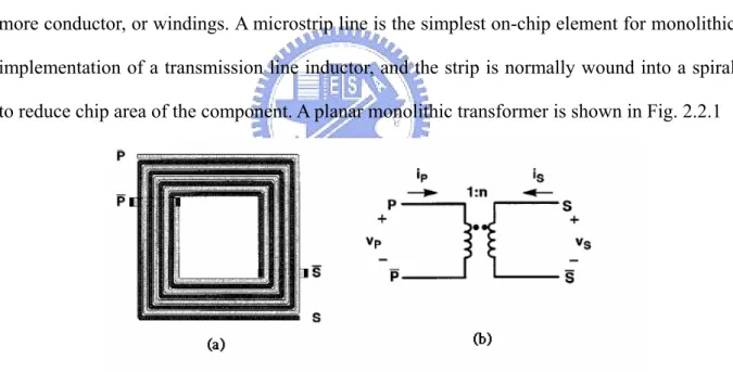
The operation of a passive transformer is based upon the mutual inductance between two or more conductor, or windings. A microstrip line is the simplest on-chip element for monolithic implementation of a transmission line inductor, and the strip is normally wound into a spiral to reduce chip area of the component. A planar monolithic transformer is shown in Fig. 2.2.1
Fig. 2.2.1 Monolithic transformer. (a) Physical layout. (b) Schematic symbol.
Magnetic flux produced by current flowing into the primary winding at the terminal P induces a current in the secondary winding that flows out of terminal S. It produces a positive voltage across a load connect between terminalSandS. The main electrical parameters of
interest are the transformer turn ratio n and the coefficient of magnetic coupling k. The current and voltage transformation of an ideal transformer are related to turns ratio by following
equation. Lp Ls i i v v n s p p s = =
= , Lp and Ls are the self-inductances of the primary and secondary
winding. The strength of the magnetic coupling between windings is defined by the k-factor.
LpLs M
k = ,where M is the mutual inductance between the primary and secondary
winding. Since the materials used in the fabrication of an IC chip have magnetic properties similar to air, there is poor confinement of the magnetic flux in a monolithic transformer. Thus, the k-factor is always substantially less than one for a monolithic transformer. The phase of the voltage induced at the secondary of the transformer depends upon the choice of the reference terminal. If the load is connected to terminal S with S grounded there is minimal
phase shift of the signal at the secondary for an ac signal source with the output and ground applied between terminals P and P . A monolithic transformer is constructed using conductors interwound in the same plane or overlaid as stacked metal. Fig. 2.2.2 show numerous transformer winding configurations.
Fig.2.2.2 Monolithic transformer winding configurations (a) Parallel conductor winding. (b) Interwound winding. (c) Overlay winding (d) Concentric spiral winding
The mutual inductance of transformer is proportional to the peripheral length of each winding. In order to maximize the periphery between windings we interleave planar metal traces or overlay conductors but it increase interwinding capacitance at the same time. The
magnetic coupling coefficient k is determined by the mutual and self-inductances, which depend primarily upon the width and spacing of the metal trace. Fig. 2.2.2(a) show a transformer with two parallel conductor which are interwound to promote coupling of the magnetic field between windings. Because the length of the primary and secondary is not equal the transformer turn ratio n≠1 although there are the same number of turns of metal
on each winding. The transformer shown in Fig. 2.2.2(b) eliminates the inherent asymmetry. This ensures that electrical characteristics of primary and secondary are identical when they have the same number of turns. Multiple conductor layers are used to fabricate an overlay or broadside coupled transformer as shown in Fig. 2.2.2(c). The stacked conductor utilizes both edge and broadside magnetic coupling to reduce the overall area in the physical layout. Flux linkages between the conductor layers is improved as the intermetal dielectric is thinned, which gives higher magnetic coefficient k when fabricated on an RF IC. The difference in thickness between metal layers results in unequal resistances for the upper and lower winding. The parasitic capacitance to the conductive substrate is different for each winding. There is a large parallel-plate parasitic capacitance between the upper and lower winding due to the overlapping if metal layers, which limits the frequency response. To reduce the parallel-plate parasitic capacitance we can offset the upper and lower metal layers by some distance d as shown in the cross-section of Fig. 2.2.2(c). Fig. 2.2.2(d) show another transformer which is implemented using concentrically wound planar spirals. The common periphery between the two windings is limited to just a single turn. Therefore, mutual coupling between adjacent conductors contributes mainly to the self-inductance of each winding and not to mutual inductance between the windings. The concentric spiral transformer has less mutual inductance and more self-inductance, which gives it a lower k-factor. However, a low ratio of mutual inductance to self-inductance is useful in applications such as peaking coils for high-performance broadband amplifiers.
2.2.3 Equivalent model of ideal transformer
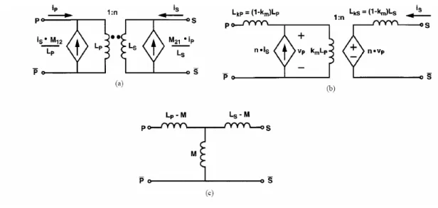
The equivalent model of an ideal transformer is shown in Fig. 2.2.3
Fig. 2.2.3. Model for magnetic coupling in a 1:n transformer. (a) Direct form model. (b) Dual-source model. (c) T-section model
In Fig. 2.2.3(a) the inductance Lp and Ls model the self-inductances of the primary and secondary windings. Mutual coupling between winding is modeled by the dependent current sources, which are weighted by the parameters M12 and M21 .The parameters M12 and M21 are
equal for a passive, reciprocal transformer. By using the Thevenize’s theory the dependent current source on the secondary side of the direct-form model gives the dual-source model shown in Fig. 2.2.3(b). Current flowing through magnetizing inductance kmLp give rise to
voltage vp which controls the dependent voltage source on the secondary side. The actual
terminal voltage is modified by current flow through leakage inductances Lkp and Lks placed
in series with the primary and secondary windings. 2 ( )( )
ks s kp p L L L L M = − − This equation
can not explicitly define two unknown leakage inductances. This arbitrary assignment of leakage inductance is not unique and other combinations are possible. The T-section model of Fig.2.2.3(c) uses three inductors to model the mutual coupling between windings. This model simplifiers hand analysis of circuits incorporating transformers, however, it is only valid for ac signals because there must be isolation of dc current flow between the primary and secondary loops in a physical transformer.
2.3 Design considerations
2.3.1 Transformer-feedback technique [3]
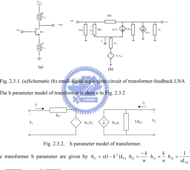
The schematic of low noise amplifier using transformer-feedback and its small-signal equivalent circuit are shown in Fig.2.3.1.
vin Zsrc Zgs Zgd gmvgs + -vgs h11 + - h12vout i1 1/h22 h21i1 ZL vout (b)
Fig. 2.3.1. (a)Schematic (b) small-signal equivalent circuit of transformer-feedback LNA The h parameter model of transformer is shown in Fig. 2.3.2
Fig. 2.3.2. h parameter model of transformer. The transformer h parameter are given by
22 22 21 12 11 2 11 1 ) 1 ( sL h n k h n k h L k s h = − = − = =
(
11 22)
11 22 L k M L L Ln= = . Impedances Zgs and Zgd represent the MOS capacitances Cgs
and Cgd. In order to realize the neutralization between the input and output the forward
11 ) 1 (g Z h Z Z G gs m gs gs i= + + ) ) 1 ( ( 11 12 h Z g Z Z h H gs m gs gs x=− + + ) / 1 || || (Z Z h22 g Ga=− m L gd ) / 1 || || )( / 1 ( 22 21g Z Z Z h h Gx=− m+ gs L gd ) / 1 || ( / 1 || 22 22 h Z Z h Z G L gd L c= +
Fig. 2.3.3. The forward signal-flow graph.
In the forward signal-flow graph we can find the primary active path consists of a voltage divider between the gate-source voltage of the transistor (path Gi),which excites the MOS
voltage-controlled current source and results in a voltage at the output node through active path Ga. Feedforward through the transformer is represent by path Gx and feedback through
the transformer by Hx. Because of inverting transformer the h12 is a negative quantity and the
feedback path subtracts from the signal applied at the input. The path Gc represent the signal
pass through the gate-drain overlap capacitance and because the overlap capacitance connects directly to an independent voltage source Vg, feedback through Cgd does not affect the
forward signal-flow graph. The condition required for neutralization is derived from the reverse signal-flow graph as shown in Fig.2.3.4.
] ) 1 ( [ || ] ) 1 ( [ || 11 11 h Z g Z Z Z h Z g Z Z H gs m gs src gd gs m gs src c + + + + + = 11 12 ) 1 ( ) || ( ) || ( h Z g Z Z Z Z Z h H gs m gs gd src gd gs x= + + +
Fig. 2.3.4. Reverse signal-flow graph
When considering the reverse signal flow, output voltage vout is an independent variable and
between the independent variable Vout and ground, they have no effect on the reverse signal
flow. From the reverse signal-flow graph we can find there are two reverse signal paths. Path Hx represents reverse signal flowing through the transformer and path Hc represents reverse
signal flowing through the gate-drain capacitance Cgd. Because h12 is a negative quantity,
these two paths can be designed to cancel to neutralize the amplifiers. Setting Hc=-Hx results
in gd gs C C k
n ≈ . For the 0.18μm CMOS technology Cgs/Cgd≈3. Therefore, neutralization is
achieved when the effective transformer turns ratio n /k is set equal to capacitance ratio
gd
gs C
C / .
2.3.2 0.7V low voltage low noise amplifier
We use the transformer feedback technique to implement a low voltage LNA and its schematic is shown in Fig. 2.3.5
Fig. 2.3.5 Schematic of low voltage LNA In order to achieve noise optimization the width of MOS is
L R C W s ox opt ω 3 1 ≈ under the
condition of power consumption-constrain. For 0.18μm CMOS technology the value of Cox is
above 8.6fF/μm2. At the operating frequency we can find the optimum widthW ≈114μm. Next select the source degeneration inductor to make sure the amplifier is stable. To achieve the neutralization the inductor Ld have to follow the rule n/k≈Cgs Cgd ≈3. The output
The transformer composted of the inductor Ls and Ld is simulated by ADS momentum. By
EM simulation we can extract the S-parameter of transformer. Thus we can find the magnetic coefficient k is ) Im( ) Im( ) Im( ) Im( 11 22 21 12 Z Z Z Z
[30] according to the four ports S-parameter of transformer. The wire connected each device is simulated by EM simulation to extract the S-parameter and used in post-simulation.
2.4 Chip implementation and measured results
2.4.1 Layout considerations
The chip layout and photo of the low voltage LNA is shown in Fig. 2.4.1. The layout skill is very important for radio frequency circuit design because it may affect circuit performance very much. In order to reduce noise , the MOSFET is used as multi-finger, which total width is 100 μm, and the power supply (Vdd) is 0.7V. The 0.18μm (minimum) gate length was chosen to get the highest speed. The MIM (Metal-Insulator-Metal) capacitors without shield and hexagonal spiral inductors (the Q-value is below 18) are used in this work. Guard-rings are added with all elements to prevent substrate noise and interference. A shielded signal GSG pad structure is used in RF input and RF output to reduce the coupling noise from the noisy substrate. All interconnections between elements are taken as a 45° corner. The RF input and the RF output are placed on opposite sides of the layout to avoid the signals coupling. The chip size is 0.84x0.63mm2.
Vss Vdd Vss Vss Vbias Vin Vout (a) (b)
Fig.2.4.1.(a) layout of transformer-feedback LNA. (b) Chip Photo of the transformer-feedback LNA
2.4.2 Measurement considerations
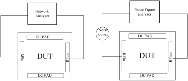
The LNA is designed for on-wafer measurement so the layout must follow the rules of CIC’s (Chip Implementation Center’s) probe station testing rules. This circuit needs one 3-pin two 3-pin DC PGP probe and two RF GSG probes for on-wafer measurement. A large coupling capacitor is needed in the input of the LNA to isolate the dc between circuit and equipment. Fig. 2.4.2 ~ Fig. 2.4.5 show the measurement setup for S-parameters, noise figure, 1dB compression point and third-order intercept point. We will discuss the experimental and simulation resultsof this circuit in following sections.
Fig. 2.4.2 Measurement setup for S-parameters Fig. 2.4.3 Measurement setup for noise figure
RF
in
RFo
ut
Fig. 2.4.4 Measurement setup for P1dB
DUT
DC PAD DC PAD Signal generation 1 Spectrum analyzer Signal generation 2 BalunFig. 2.4.5 Measurement setup for IIP3
2.4.3 Measurement results and discussions
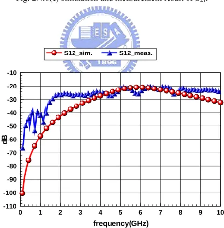
This work is designed and processed using TSMC 0.18µm mixed-signal/RF CMOS 1P6M technology. The simulation and measurement S-parameter are shown in Fig. 2.4.6(a) ~ (d), noise figure is shown in Fig. 2.4.7, P1dB is shown in Fig. 2.4.8 and IIP3 is shown in Fig. 2.4.9.
0 1 2 3 4 5 6 7 8 9 10 frequency(GHz) -25 -20 -15 -10 -5 0 d B S11_Sim. S11_Meas.
Fig. 2.4.6(a) simulation and measurement result of S11.
0 1 2 3 4 5 6 7 8 9 10 frequency(GHz) -35 -30 -25 -20 -15 -10 -5 0 d B S22_sim. S22_meas.
0 1 2 3 4 5 6 7 8 9 10 frequency(GHz) -40 -35 -30 -25 -20 -15 -10 -5 0 5 10 d B S21_sim. S21_meas.
Fig. 2.4.6(c) simulation and measurement result of S21.
0 1 2 3 4 5 6 7 8 9 10 frequency(GHz) -110 -100 -90 -80 -70 -60 -50 -40 -30 -20 -10 d B S12_sim. S12_meas.
3 4 5 6 7 8 frequency(GHz) 2 4 6 8 10 12 14 16 nf_sim nf_meas
Fig. 2.4.7 simulation and measurement result of NF.
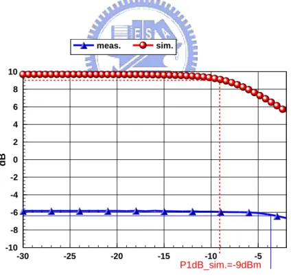
-30 -25 -20 -15 -10 -5 -10 -8 -6 -4 -2 0 2 4 6 8 10 d B meas. sim. P1dB_sim.=-9dBm P1dB_meas.=-4.8dBm Fig. 2.4.8 simulation and measurement result of P1dB.
-20 -15 -10 -5 0 5 10 RF power(dBm) -70 -60 -50 -40 -30 -20 -10 0 10 IIP3_meas. IIP3_sim. IIP3_sim=-3dBm IIP3_meas=8dBm
Fig. 2.4.9 simulation and measurement result of IIP3.
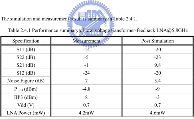
The simulation and measurement result is summary in Table 2.4.1.
Table 2.4.1 Performance summary of low-voltage transformer-feedback [email protected]
Specification Measurement Post Simulation
S11 (dB) -14 -20 S22 (dB) -5 -23 S21 (dB) -1 9.8 S12 (dB) -24 -20 Noise Figure (dB) 7 3.4 P1dB (dBm) -4.8 -9 IIP3 (dBm) 8 -3 Vdd (V) 0.7 0.7 LNA Power (mW) 4.2mW 4.6mW
The measurement results reveals that the output is not match to 50Ω thus the power can not transmit out. We find the possible problem from the layout of circuit. In layout the four ports of the transformer composed of LS and Ld are connected to the MOS source node, drain node,
Vdd pad and Vss PAD. There are no connections between all Vss PAD. Because of the isolation
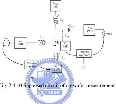
of each Vss PAD these ground nodes are no longer perfect grounded. Although we use external equipment to connect this Vss PAD between ground, it could induced parasitical effect along the ground path and influence the measurement data. The parasitic impedance arises from the external measure machine. The figure 2.4.10 shows the supposed circuit under the situation of on-wafer measurement.
Vin PAD Ld Ls M1 Vout PAD VDD PAD Lg Cd Cout Vss PAD Vss PAD Parasitic impedance Parasitic impedance ~ Vin 50Ω
Fig. 2.4.10 Supposed circuit of on-wafer measurement
The modified simulation gives us a reasonable explanation the difference between simulation and measurement. The Fig.2.4.11(a)~(d) shows the modified simulation result and on-wafer measurement result.
0 1 2 3 4 5 6 7 8 9 10 GHz -20 -18 -16 -14 -12 -10 -8 -6 -4 -2 0 d B S11_modify S11_meas.
Fig.2.4.11(a) the modified simulation and on-wafer measurement result of S11.
0 1 2 3 4 5 6 7 8 9 10 GHz -12 -10 -8 -6 -4 -2 0 d B S22_modify S22_meas.
0 1 2 3 4 5 6 7 8 9 10 GHz -45 -40 -35 -30 -25 -20 -15 -10 -5 0 5 d B S21_modify S21_meas.
Fig.2.4.11(c) the modified simulation and on-wafer measurement result of S21
0 1 2 3 4 5 6 7 8 9 10 GHz -110 -100 -90 -80 -70 -60 -50 -40 -30 -20 -10 d B S12_modify S21_meas.
Fig.2.4.11(d) the modified simulation and on-wafer measurement result of S12
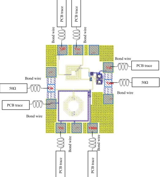
According to the above figures it can be found that the issue of non-connection between Vss PAD is the possible problem of this circuit. Thus we use the external PCB board to connect the Vss PAD. The PCB trace and bond wire induce additional parasitical effect. The trace on the board can be approximate microstrip line. The height of substrate is 0.8mm,
dielectric is 4.4 and loss tangent is 0.02. The metal is copper which conductivity is 5.8x10⁷. The inductor of bond wire is above 0.8nH/mm. The Fig. 2.4.12 shows the approximately simplified circuit of the chip bonded on PCB board. The PCB layout is shown in Fig. 2.4.13. The photo of the PCB board and bonded chip is shown in Fig.2.4.14
We consider the bond-wire and PCB-trace effect and the modified simulation result are shown in Fig. 2.4.15(a)~(d). The modified simulation and PCB board measurement results of S11 ,S22
and S12 have the same pattern although it still exist a little difference.
Vss Vdd Vss Vss Vbias Vin Vout PCB tr ace PCB tr ace PCB trace 50Ω PCB tr ace PCB tr ace PCB trace 50Ω Bond wire Bo nd wi re Bo nd wi re Bond wire Bond wire Bond wire Bond w ire Bond wire
Fig. 2.4.13 PCB layout
Fig. 2.4.14 (a) photo of PCB board Fig. 2.4.14 (b) photo of bonded chip.
0 1 2 3 4 5 6 7 8 9 10 GHz -16 -14 -12 -10 -8 -6 -4 -2 0 2 d B S11_modified S11_PCB_meas.
0 1 2 3 4 5 6 7 8 9 10 GHz -40 -35 -30 -25 -20 -15 -10 -5 0 d B S22_modified S22_PCB_meas.
Fig. 2.4.15 (b) modified and PCB_meas. result of S22.
0 1 2 3 4 5 6 7 8 9 10 GHz -100 -90 -80 -70 -60 -50 -40 -30 -20 -10 d B S12_modified S12_PCB_meas.
0 1 2 3 4 5 6 7 8 9 10 GHz -50 -40 -30 -20 -10 0 10 d B S21_modified S21_PCB_meas.
Fig. 2.4.15 (d) modified and PCB_meas. result of S21.
2.4.4 Comparisons
Table 2.4.2 shows the comparisons of this work simulation result and recent LNA papers.
Table 2.4.2 The comparisons of this work simulation result and recent LNA papers.
Tech. Freq. (GHz) S11(dB) S22(dB) S21(dB) NF(dB) IIP3 (dBm) Vdd(V) Power (mW) this work 0.18μm CMOS 5.8 -20 -24 10.2 3.4 -3 0.7 4.6 [27] 0.18μm CMOS 5 -15 -21 20 1.4 -29 0.65 1.9 [3] 0.18μm CMOS 5.75 <-10 -8 14.2 0.9 0.9 1 16 [28] 0.18μm CMOS 5.8 -5.3 -10.3 13 2.5 - 1 22
Chapter 3 3.1-10.6GHz CMOS Ultra-wideband low
noise amplifier
3.1 Introduction
The ultra-wideband (UWB) system is a new wireless technology capable of transmitting data over a wide spectrum of frequency bands approved by Federal Communication Commission (FCC) in 2002. Because the UWB system transmits information using very low power and high date rate over a wide band, it becomes more and more popular for wireless communication. The UWB standard IEEE 802.15.3a is defined by FCC, and most of the proposed applications are allowed to transmit in a band between 3.1- 10.6GHz due to its versatility in almost all of the approved UWB application. Because FCC doesn’t define all spectrums completely various methods can be employed to utilize the vast spectrum. Two proposal have been refined for the final decision: Direct-sequence UWB(DS-UWB) and multi-band orthogonal frequency division multiplexing UWB(MB-OFDM UWB). The DS-UWB divides the 3.1-10.6GHz band into two discontinuous bands while the MB-OFDM UWB proposal divides the whole band into 14 528-MHz sub-bands that are grouped into five main bands. In many ways, UWB benefits from existing wireless techniques and standards, as modulation schemes, multiple-access techniques, and transmitter/receiver architectures are adapted for UWB.
3.2 Numerous topology of UWB LNA
The noise performance of an LNA is directly dependent on its input matching. The wide-band input matching is intrinsically noisier than narrow-band counterparts as the noise performance can not be optimized for a specific frequency. Thus the designer has to be trade off between
the input matching and noise. The Fig. 3.2.1 shows four basic 50Ω input matching techniques[5][6][7][8][9].
Fig. 3.2.1 Basic input matching topology. (a)Inductive source degeneration.(b)Direct resistor termination.(c)Shunt-series feedback.(d)Common-gate 1/gm termination
The four input matching is only suit for narrow band amplifier. In wireless mobile communications systems, silicon integrated circuits have been widely employed in narrow-band systems, where limited gain and increased parasitic is tolerable due to lower operation frequency and the application of tuned networks.
There are few examples of development of high-frequency wideband amplifiers employing silicon transistors, in particular in CMOS technology.
z Distributed amplifiers [10]
Fig. 3.2.2 Basic four single-end distributed amplifier
The distributed amplifiers normally provide wide bandwidth characteristics but they consume large dc current due to the distribution of multiple amplifying stages, which make them unsuitable for low-power application. And the distributed amplifiers are not optimized for noise. This bring the challenge of finding a low-power topology that satisfies all the other design requirements, the most stringent one being the input match.
z Resistive shunt-feedback amplifiers
In Fig. 3.2.3 a conceptual schematic of a shunt feedback amplifier is shown[11].
Fig. 3.2.3 Conceptual schematic of a shunt feedback amplifier.
resistance divided by the loop-gain of the feedback amplifier. The input impedance is ⎥⎦ ⎤ ⎢⎣ ⎡ + + + = ) 1 ( 1 ) 1 ( ) ( A R s A R s Z f f
in ,where the gain A is chosen such that Rf (1+ )A =Rs .The
resistive shunt-feedback amplifier has better bandwidth than conventional low noise amplifier but it has limited input match at higher frequencies due to the parasitic input capacitance. As consequence, the maximum input capacitance that can be tolerated to achieve an input reflection coefficient equal to -10dB at ƒ = 10 GHz is as low as
(
)
2(
2)
1
1 Γ − Γ
= R f
C π s =200fF. To satisfying this requirement with a CMOS amplifier
stage while achieving sufficient gain and low noise is difficult. Some paper has been present by using this topology over the low band of UWB(3-5GHz)[12] shown in Fig.3.2.4.
Fig. 3.2.4 UWB LNA topology. (a) Overall schematic. (b) Small-signal equivalent circuit at the input.
In this topology, one of the key role of the feedback resistor Rf is to reduce the Q-factor of the
resonating narrowband LNA input circuit. The Q-factor of the circuit can be approximately given by gs fM g s t WB C R L L Rs Q ⋅ ⋅ ⎥ ⎥ ⎦ ⎤ ⎢ ⎢ ⎣ ⎡ + + ≈ 0 2 0 ) ( 1 ω ω ω
. According to this equation, the
selection of Rf. The feedback resistor helps to extend the bandwidth of the amplifier as well as
the gain flatness, while contributing a small amount in NF degradation.
z Ultra-wideband low noise amplifier using LC-ladder filter input matching network [11][13]
Recently another topology of wideband LNA has been present. It expands the conventional narrow-band LNA using source degeneration by embedding the input network of the amplifying device in a multisection reactive network so that the overall input reactance is resonated over a wider bandwidth. Fig. 3.2.5 shows a typical narrowband cascade LNA topology and its small-signal equivalent circuit.
Fig. 3.2.5. Narrowband LNA topology. (a) overall schematic. (b) Small-signal equivalent circuit at the input The inductor Ls is added for simultaneous noise and input matching and Lg for the impedance
matching between the source resistance Rs and the input of the narrowband LNA[14]. Fig.
3.2.5(b) shows the equivalent small-signal circuit. Assume the gate-drain Cgd can be ignore
the impedance of the gate terminal is a series RLC circuit. The reactive part of the input impedance is resonated at the carrier frequency in narrowband design. The basic concept of the LC-ladder input matching is expanded from the input impedance of the narrowband which is a series RLC circuit. Consider a fourth-order bandpass ladder filter, shown as in Fig. 3.2.6.
Fig. 3.2.6 Fourth-order bandpass ladder filter used for impedance matching.
The right part of the bandpass filter looks similar to the equivalent circuit of the inductively degenerated transistor in Fig. 3.2.5(b). Therefore, the bandpass filter can embed the inductively degenerated transistor and obtain the desire input impedance. The LC-ladder filter input matching of wideband LNA has two significant drawbacks. Because the LC-ladder filter at the input mandates a number of reactive elements, which could lead to a larger chip area and noise figure degradation in the case of on-chip implementation.
z Ultra-wideband low noise amplifier using the common-gate as the first stage.[15]
The common-gate architecture that is illustrated in Fig. 3.2.1(d) has highest potential to achieve the wide-band input matching. In traditional narrow-band receiver the common-gate is not used widely due to its relatively lower gain and higher noise figure than a common-source amplifier. The actual configuration of common-gate stage is shown in Fig. 3.2.7(a).
Fig. 3.2.7 (a) Configuration of a common-gate input stage. (b) The small-signal equivalent circuit.
From the Fig. 3.2.7(b),we can derive the input impedance ) ( ) ( 1 ) ( 1 1 ) ( ) ( 1 ) ( 1 1 1 1 1 1 ω ω ω ω ω ω m s o m oo o o o m s m in jX R X jg X j g Z R Z g Z g Z + − + − ≅ + − + + =
In below equation we assume that the Zs(ω) and Zo(ω) are both composed of high-Q
inductors and capacitors and can be regarded as purely reactive within the frequency band of
interest. // // ( ) C j 1 ) ( Z , ) ( 1 // ) ( 2 gd o ω ω ω ω ω ω ω s L in o gs s jX Z Z jX C j Ls j Z = = = =
After some mathematical calculation
)) ( ) ( 1 ) ( 1 ( ) ) ( ) ( . ( 1 2 2 1 2 2 2 1 1 ω ω ω ω ω o o o o m s o o o o m m in X X R R g X j X R R X g g Z ⋅ + + + − + − − =
Since gm1Xo2(ω)<<Ro2+Xo2(ω),the real part in the denominator will remain relatively
constant within the 3.1-10.6GHz UWB band. The imperfect matching of the common-gate stage throughout the band arise from the frequency dependent Xs(ω) that dominates the imaginary part in the denominator. To get a good matching over the wide band , the LC tank of Xs(ω) formed by Ls and Cgs should be selected such that they resonate at the center of the
3.1-10.6GHz, leaving only a 50Ω real input impedance. The noise figure of the common-gate input stage UWB LNA can be improved by increasing gm1 but it will degrade the input
matching.
z Reactive-feedback wideband amplifier [16][17]
An alternate approach to the modified UWB LNA is a negative-feedback amplifier. Feedback offers numerous benefits for broadband application, including gain, stability over processing and supply variations, lower distortion and the ability to get port impedances for noise and impedance matching. However the simple feedback stage is difficulty to achieve a 50Ω input match, low noise figure and low power consumption in simultaneous. Broadband resistive feedback also meets the bandwidth target, but the reactive-feedback using transformer contributes less noise as losses are relatively small in the transformer windings. The
schematic shown in Fig. 3.2.8 is present recently [16].
Fig. 3.2.8 Reactive feedback UWB LNA.
The transformer in the first stage give a broadband input match without multi-inductor network which will add noise and require more chip area. The current-reuse is also approved in this design for lower DC power consumption. The transformer of second stage provides a broadband output match relatively close to 50Ω so the output buffer is not need for output match.
z Wideband matching using the transistor intrinsic gate-drain capacitor [18]
Recently a novel wideband input match has been present. It considers the gate-drain capacitor has significant effect on the circuit performance. The Fig. 3.2.9 show a simple common source amplifier with source degeneration inductor and the drain loaded an equivalent capacitor and resistor from the next stage.
Fig. 3.2.9 The small signal equivalent circuit of common-source with inductive source degeneration
The Cgd and ro are neglected in conventional analysis of low noise amplifier. It is inaccurate
numerically. If both Cgd and ro are considered we will find that the input match at high
frequency is depend on the resistive load and at low frequency is depend on the capacitive load. We can achieve wideband match without external input match network. It also can achieve low noise match.
3.3 Design consideration
3.3.1 Wideband match technique[18]
Consider a small signal equivalent circuit of a source degeneration low noise amplifier which is shown in Fig.3.3.1 CL and RL present the parasitic capacitance and resistance which
is contributed from the next stage.
Fig. 3.3.1 The small signal equivalent circuit of source degeneration
To derive the input impedance we consider that the load of the circuit is divided into two parts, one of which is only a resistor RL which dominates at the high frequency and another is the
capacitor CL dominates at the low frequency. The circuit of resistive loading is shown in Fig.
RL Cgd Cgs Ls ro + -vgs gmvgs Zin
Fig. 3.3.2 The equivalent small signal circuit of resistive loading
While we assume that s L
gs
s L R
C
L << ω <<
ω
ω 1 we can find the input impedance
1 )] 1 ( 1 )[ 1 ( + + + − ≈ m L gs gd gs m s gs in g R C C C g L C j Z γ γ ω , with o L s o L j R r r ω γ + + = . As frequency as high
the input impedance will approach the 50Ω when the inductor Ls is designed properly. To derive the input impedance of the capacitive loading, which is shown in Fig.3.3.3, we divided this circuit into two branches and replace the current source by voltage source.
Fig. 3.3.3 The equivalent circuit with capacitive loading
One of the two branches is looking into the capacitor Cgs and another is looking into the
capacitor Cgd. Yα is the impedance looking into the Cgd and Zβ is the impedance looking into
the Cgs. Assuming that the current flowing the capacitor Cgd and Cgs is smaller than the
induced current gmVgs, the Yα can be derived. Thus = +( + 1 + α)−1 α α α ω ω jωL C j R C j Y gd and 1 ) 1 1 ( 1 + + + − = β β β β ω ω ω L j C j R C j Z gs
with (1 m o) gd o m L S gd o m gd m L g r C r g C L L C r g C C g C Rα = α = α = + gs L o m s o m gs gs s m C C r g L L r g C C C L g Rβ = β = β =
The input impedance of the capacitive loading circuit can be found out as follow
1 ) 1 ( + − = β α Z Y
Zin . According to above the equations the input impedance can be rearranged as
a simpler RLC circuit as shown in Fig.3.3.4.
Rα Cα Lα
Cgs Cgd
Rβ
Cβ
Lβ
Fig. 3.3.4 the equivalent circuit of the input impedance
The Cgd branch is the critical branch that is a series component of RLC and its resonate
frequency is ) 1 ( 2 1 2 1 0 o m L SC g r L C L f + = = π
π α α . At the high frequency the resistive
loading is matched and the capacitive loading is matched at the comparatively low frequency. Thus the composite RLCL load circuit is matched over a wide bandwidth.
3.3.2 3.1-10.6GHz CMOS Ultra-wideband low noise amplifier
Fig. 3.3.5 shows a UWB LNA using transistor’s intrinsic gate-drain capacitor to achieve input matching. In this design we add an inductor to the original RLCL loading circuit, as
Fig. 3.3.5 The schematic of proposed UWB LNA Ls CL RL Li Cex Rd Ld Vdd
Fig. 3.3.6 The equivalent circuit of the first stage UWB LNA
In this circuit the external Cex is added to increase the equivalent gat-drain capacitance, thus
allowing a smaller transistor to get better input match but it effect the noise figure at lower frequency. The inductor Li can improve the input matching. From the simulation result we can
find add the inductor can help S11 contour around the original point (i.e. 50Ω ) in the smith
freq (100.0MHz to 12.00GHz) S( 1, 1 ) L=0nH freq (100.0MHz to 12.00GHz) S( 1 ,1 ) L=2nH freq (100.0MHz to 12.00GHz) S (1, 1) L=1.5nH freq (100.0MHz to 12.00GHz) S( 1 ,1 ) L=2.5nH Fig. 3.3.7 The input return loss for different Li
To improve the input match at lower frequency the gate inductor is added and it will influence the noise figure. Shunt-series-peaking is a bandwidth extension technique [19] which is used in this circuit to extend bandwidth by the inductor Ld, Li and resistor Rd. To achieve a flat gain
over whole frequency range we cascade three stages.
The concept of this design is that we design the first stage with a capacitive, resistive and inductive load to achieve the input return loss first. The transformer is added to improve the input retune loss and flatter gain but it may make the circuit become a little unstable and it has to be design carefully. The value of capacitive load is approximated to the next input impedance of next stage. Due to the input impedance of the common source topology is the series resistance, capacitor and inductor it is suited to be the consequence stage. We use the common source topology to be the second and third stage. Then we replace the resistance by
the common source stage with a capacitive, inductive and resistive load and fine tune all element to get input return loss and output return loss. And the third stage is designed by the same way. Finally we fine tune the drain inductor to improve the flatter gain. The three stages are response for different band of gain to maintain the flatter gain over whole wide band.
3.4 Chip implementation and measurement results
3.4.1 Layout considerations
The chip layout and photo of the UWB LNA is shown in Fig. 3.4.1. The power supply (Vdd) is 1V. The 0.18μm (minimum) gate length was chosen to get the highest speed. The MIM (Metal-Insulator-Metal) capacitors without shield and hexagonal spiral inductors (the Q-value is below 18) are used in this work. Guard-rings are added with all elements to prevent substrate noise and interference. A shielded signal GSG pad structure is used in RF input and RF output to reduce the coupling noise from the noisy substrate. All interconnections between elements are taken as a 45° corner. The RF input and the RF output are placed on opposite sides of the layout to avoid the signals coupling. The chip size is 1.314x0.89mm2. All connection wire are simulated by ADS momentum to extract parasitical effect.
(b)
Fig. 3.4.1(a) chip layout (b) chip photo of UWB LNA.
3.4.2 Measurement considerations
The UWB LNA is designed for on-wafer measurement so the layout must follow the rules of CIC’s (Chip Implementation Center’s) probe station testing rules. This circuit needs four 3-pin DC PGP probe and two RF GSG probes for on-wafer measurement. A large coupling capacitor is needed in the input of the LNA to isolate the dc between circuit and equipment. Fig. 3.4.2 ~ Fig. 3.4.5 show the measurement setup for S-parameters, noise figure, 1dB compression point and third-order intercept point. We will discuss the experimental and simulation resultsof this circuit in following sections.
Fig. 3.4.2 Measurement setup for S-parameters Fig. 3.4.3 Measurement setup for noise figure
RF
in
RFo
ut
Fig. 3.4.4 Measurement setup for P1dB
DUT
DC PAD DC PAD Signal generation 1 Spectrum analyzer Signal generation 2 BalunFig. 3.4.5 Measurement setup for IIP3
3.4.3 Measurement results and discussion
The Ultra-wideband low noise amplifier is simulated by ADS. The simulation and measurement results are shown in Fig. 3.4.6(a)~(d), where the simulation S11 < -10dB and
S22<-10dB from 3.1GHz to 10.6GHz. The simulation maximum and minimum power gain
0 2 4 6 8 10 12 14 16 18 20 frequenc(GHz) -40 -35 -30 -25 -20 -15 -10 -5 0 5 d B S11_sim. S11_meas.
Fig. 3.4.6(a) simulation and measurement result of S11
0 5 10 15 20 frequency(GHz) -45 -40 -35 -30 -25 -20 -15 -10 -5 0 d B S22_sim. S22_meas.
0 2 4 6 8 10 12 14 16 frequenc(GHz) -200 -180 -160 -140 -120 -100 -80 -60 -40 -20 d B S12_sim. S12_meas.
Fig. 3.4.6(c) simulation and measurement result of S12
0 2 4 6 8 10 12 14 16 frequenc(GHz) -40 -35 -30 -25 -20 -15 -10 -5 0 5 10 15 d B S21_sim. S21_meas.
3 4 5 6 7 8 9 10 frequency(GHz) 4 6 8 10 12 14 nf_sim nf_meas
Fig. 3.4.6(e) simulation and measurement result of NF
The simulation and measurement result of P1dB are shown in Fig. 3.4.7 (a)~(c).
-30 -25 -20 -15 -10 -5 0 5 10 input power(dBm) -25 -20 -15 -10 -5 0 5 10 15 d B P1dB_sim P1dB_meas P1dB_sim.=-15dBm P1dB_meas.=2.5dBm
f=4.1GHz
-30 -25 -20 -15 -10 -5 0 5 10 input power(dBm) -25 -20 -15 -10 -5 0 5 10 15 d B P1dB_sim P1dB_meas P1dB_sim.=-14.8dBm P1dB_meas.=4dBm
f=6.1GHz
Fig. 3.4.7(b) simulation and measurement result of P1dB at 6.1GHz
-30 -25 -20 -15 -10 -5 0 5 10 input power(dBm) -20 -15 -10 -5 0 5 10 15 d B P1dB_sim P1dB_meas P1dB_sim.=-13dBm P1dB_meas.=5.5dBm
f=8.1GHz
The simulation and measurement results of IIP3 are shown in Fig. 3.4.8(a)~(f) -30 -25 -20 -15 -10 -5 0 5 dBm -70 -60 -50 -40 -30 -20 -10 0 IIP3_sim. [email protected]=-7dBm -20 -15 -10 -5 0 5 dBm -80 -70 -60 -50 -40 -30 -20 -10 IIP3_meas. [email protected]=6dBm
Fig. 3.4.8 (a) the simulation of IIP3 at 4.1GHz (b) the measurement result of IIP3 at 4.1GHz
-30 -25 -20 -15 -10 -5 0 5 dBm -70 -60 -50 -40 -30 -20 -10 0 IIP3_sim. [email protected]=-6dBm -20 -15 -10 -5 0 5 dBm -80 -70 -60 -50 -40 -30 -20 -10 IIP3_meas. [email protected]=5.5dBm
-30 -25 -20 -15 -10 -5 0 5 dBm -80 -70 -60 -50 -40 -30 -20 -10 0 10 IIP3_sim. [email protected]=-4dBm -20 -15 -10 -5 0 5 dBm -70 -60 -50 -40 -30 -20 -10 IIP3_meas. [email protected]=6.8dBm
Fig. 3.4.8 (e) the simulation of IIP3 at 8.1GHz (f) the measurement result of IIP3 at 8.1GHz The simulation and measurement result is summary in Table 3.4.1.and comparison with recent papers in Table 3.4.2.
Table 3.4.1 Performance summary of Ultra-wideband LNA
Specification Measurement Post Simulation
S11 (dB) <-5 <-10
S22 (dB) <-5 <-10
S21 (dB) -10(average) 12dB(flat gain)
S12 (dB) <-30 <-40
Noise Figure (dB) 5(min) 4.5(min.)
4.1GHz 6.1GHz 8.1GHz 4.1GHz 6.1GHz 8.1GHz P1dB (dBm) 2.5 4 5.5 -15 -15 -13 IIP3 (dBm) 6 5.5 6.8 -7 -6 -4 Vdd (V) 1 1 LNA Power (mW) 17 18.12
Table 3.4.2 The comparisons of this work simulation result and recent LNA papers. Tech. BW (GHz) S11 (dB) S22 (db) Flat Power Gain (dB) NFmin (dB) VDD (V) Power (mW) This work simulation 0.18μm CMOS 3.1-10.6 <-10 <-10 12.5 4.5 1 18 [29] 0.18μm CMOS 2-6.5 <-7.8 N/A 11.9 4.1 1.8 27 [16] 0.13μm CMOS 3.1-10.6 <-9.9 <-6.2 15.1 2.5 1.2 9 [11] 0.18μm CMOS 2.4-9.5 < -9.4 < -10 10.4 4 1.8 9 [15] 0.18μm CMOS 3.1-10.6 <-9 <-13 15.9-17.5 3.1-5.7 1.8 33.2 [17] 0.18μm CMOS 3.1-10.6 <-10 <-10 10.87-12.0 4.7 1.5 10.57 The measurement results reveal that the input return loss is not good and no power gain.
We consider the layout of the UWB LNA to find the possible problem. The simplified chart of layout is shown in Fig. 3.4.9.
Fig. 3.4.9 simplified chart of UWB LNA layout
connect each other by external measurement machine and along this path may be suffer from some unknown parasitical impedance. Thus it lets the expected ground node to become imperfect ground. We add this parasitic impedance at this Vss node and the modified simulation can reveal that the imperfect ground may effect the performance of this UWB LNA, which is shown in Fig. 3.4.10(a)~(d).
0 2 4 6 8 10 12 14 16 18 20 GHz -35 -30 -25 -20 -15 -10 -5 0 5 d B S11_modified S11_meas.
Fig. 3.4.10(a) modified and measurement result of S11.
0 2 4 6 8 10 12 14 16 18 20 GHz -45 -40 -35 -30 -25 -20 -15 -10 -5 0 d B S22_modified S22_meas.
0 2 4 6 8 10 12 14 16 18 20 GHz -40 -35 -30 -25 -20 -15 -10 -5 0 5 10 15 d B S21_modified S21_meas.
Fig. 3.4.10(c) modified and measurement result of S21
0 2 4 6 8 10 12 14 16 18 20 GHz -160 -140 -120 -100 -80 -60 -40 -20 d B S12_modified S21_meas.
Fig. 3.4.10(d) modified and measurement result of S12
According to the above figures it can be found that the issue of non-connection between Vss PAD is the possible problem of this circuit. Thus we use the external PCB board to