沉積後電漿處理與退火製程對二氧化鉿熱穩定性之影響
84
0
0
全文
(2) 沉積後電漿處理與退火製程對二氧化鉿熱穩定 性之影響. The effects of the plasma treatment and the annealing process on the thermal stability of HfO2 dielectrics. 研 究 生:湯鈞凱. Student:Chun-Kai Tang. 指導教授:汪大暉 博士. Advisor:Dr. Ta-Hui Wang. 國 立 交. 通 大 學. 電機學院微電子奈米科技產業研發碩士班 碩. 士. 論. 文. A Thesis Submitted to College of Electrical and Computer Engineering National Chiao Tung University in partial Fulfillment of the Requirements for the Degree of Master in Industrial Technology R & D Master Program on Microelectronics and Nano Sciences February 2008, Hsinchu, Taiwan, Republic of China. 中華民國九十七年二月.
(3) 沉積後電漿處理與退火製程對二氧化鉿熱穩定 性之影響. 研究生:湯鈞凱. 指導教授:汪大暉 博士. 國立交通大學電機學院產業研發碩士班. 摘要 隨著 CMOS 技術急速的微縮到奈米技術點,傳統閘極介電層二氧化矽層將 達到其物理與電性限制。主要的問題是的量子效應引發無法接受的大量的载子直 接穿隧電流(Direct Tunneling Current)穿隧超薄二氧化矽層。為了可以有效的 抑制此漏電流,高介電常數的閘極介電層材料會被使用來取代傳統的二氧化矽層 而可以維持在相同的等效電性氧化層厚度(EOT)下增加實際介電層膜的厚度。 隨著金氧半場效電晶體的微縮,二氧化矽當作閘極介電層將面臨到物理限制。當 互補式金氧半場效電晶體的閘極通道長度微縮到 100 奈米以下時,閘極介電層的 有效電性厚度將縮小至 1.2 奈米以下,以二氧化矽當作氧化層將會面臨到很多的 挑戰,影響最嚴重的就是超薄厚度之二氧化矽絕緣膜其直接穿遂電流將大到無可 忍受的程度,因此需要高介電係數材料來取代二氧化矽作為閘極氧化層。高介電 係數氧化層可以擁有較厚的物理厚度而維持相同的等效氧化層厚度來抑制穿遂 電流的形成。其中以金屬鉿為主的材料被認為是目前最有可能來取代二氧化矽。 本實驗以鋁-鈦-HfO2-矽之MIS結構為分析元件。首先,我們利用金屬有機物化學 氣相沉積方法分別在矽晶片上沉積HfO2,然後進行不同溫度的沉積後退火步驟, i.
(4) 找出最適當的退火溫度。接著再分別進行表面電漿處理以及電漿後的退火步驟。 接著,我們進行 600 度 60 秒的高溫快速熱退火。最後,我們進行 800~900 度 30 秒的高溫處理,我們利用量測C-V和I-V曲線去探討薄膜的基本特性。另外藉由 磁滯效應、SILC特性、CVS測試和變溫測試來討論經過電漿處理和沒有經過電 漿處理元件的可靠度分析。我們可以發現經過電漿處理的試片可以承受較高的溫 度卻不會降低原本的電容值。這是因為電漿源中的氮原子可以抑制介電層和矽之 間的氧化層成長。. ii.
(5) The effects of the plasma treatment and the annealing process on the thermal stability of HfO2 dielectrics. Student:Chun-Kai Tang. Advisor:Dr. Ta-Hui Wang. Industrial Technology R & D Master Program of Electrical and Computer Engineering College National Chiao Tung University. ABSTRACT As CMOS devices are scaled aggressively into nanometer regime, SiO2 gate dielectric is approaching its physical and electrical limits. The primary issue is the intolerably huge leakage current caused by the direct tunneling of carriers through the ultrathin oxide. To substantially suppress the leakage current, high-k materials are recently employed by exploiting the increased physical thickness at the same equivalent oxide thickness (EOT). The aggressive scaling of MOS devices is quickly reaching the fundamental limits of SiO2 as the gate insulator. When the gate oxide thickness scales down below 1.2 nm for 100 nm-node CMOS technology and beyond and the SiO2 will face severe challenges such as the direct-tunneling current. Therefore, high dielectric constant gate oxides with large physical thickness while identical equivalent oxide thickness (EOT) have been used to replace SiO2 in order to reduce gate leakage current. HfO2 dielectric is a most suitable material for future MOSFET gate oxide applications. In this study, we analysis the Al/ Ti/ HfO2 /Si MOS structure. First, we deposited HfO2. iii.
(6) and on Si wafers individually by metal-organic CVD (MOCVD) system. Then, the films received different post-deposition-annealing temperature. After PDA, we had additional plasma treatment and post-nitridation annealing 600℃ 60 sec (PNA). Next, we treated the films with high temperature 800℃, 850℃ and 900℃ 30 sec. The electrical characteristics of the film were discussed by C-V and I-V curves. The reliability of the film with nitridation or not were discussed by hystersis effect, SILC( Stress Induce Leakage Current), CVS(Constant Voltage Stress) test and measure at different temperature. We could find that that the film with nitridation could sustain high thermal stress, and its capacitance did not decrease. It might be that nitrogen could suppress the formation of interfacial layer between the high-k/Si interface.. iv.
(7) 誌謝 時間過得真快,兩年的研究所生活即將結束。首先要感謝我的指 導老師汪大暉教授與張國明教授,除了給予我正確的研究方法與專業 的教導,建立深厚的研究基礎,讓我受益良多之外,老師也常常告訴 我們做人處事的道理,並常常鼓勵我們、支持我們。 其次感謝實驗室學長的熱心指導,尤其是陳柏寧和林建宏學長, 是你們在我遇到困難及問題時,適時給予寶貴的意見,也感謝學弟在 實驗上的協助,使得我的論文可以很順利的完成。另外,我要感謝國 家奈米元件實驗室與交大奈米中心提供良好的設備和每一位勞苦功 高的工作人員所給予的幫助,讓我能順利的完成實驗。謝謝! 在研究所的期間,我要感謝實驗室同學們的幫忙與照顧,另外還 要感謝我的好朋友們,因為你們讓我的碩士生活更精采更順利。 最後,本論文獻給我最敬愛的父母湯世榮先生、韓秀芬女士,感 謝他們多年來辛苦的栽培和養育,當我遇到困難的時候,給予全力的 幫助與支持,達成今日的成就,謝謝你們。 這兩年回憶,是我和你們大家一起完成的故事,記錄在這本論文裡。 這本論文,獻給大家。謝謝你們~. v.
(8) Contents Chinese Abstract ...........................................................................................................i English Abstract ......................................................................................................... iii Acknowledgments .........................................................................................................v Contents ......................................................................................................................vi Table Captions ..............................................................................................................ix Figure Captions.............................................................................................................ix. Chapter 1. Introduction. 1.1 Motivation to Study High-k Dielectrics….….….….…..……………..................................……...…1 1.2 Scaling of the Gate Oxide Thickness............................................................................………3 1.3 Roadmap of the Gate Dielectric..................... 1.4 The Need to Use High-k Materials. .....................................................................………...4. .................... .............................................................……….…5. 1.4.1 Motivation to Study High-k Dielectrics…………...……………...…………...…………5 1.4.2 The advantages of High-k Dielectric…………....………..…………………………………7 1.4.3 The choice of High-k Materials…………….…………………………………………….…8 1.4.4 Why choose HfO 2 …………………...…………………………………...…………......…10 1.5 Plasma Nitridation………………… .....................................................…………….... 11 1.6 Thesis Organization…......………........................................……………………………….... 12. vi.
(9) Chapter 2. Experiments of Al /Ti /HfO2 /Si MIS Capacitor. 2.1 The methods to prepare High-K thin film.............................................................................13 2.1.1 MOCVD..............................................................................................................................................................13 2.1.2 DC Magnetron Sputtering.................................................................................................................15 2.2 Rapid Thermal Annealing system...............................................................................................................15 2.3 Plasma treatment system....................................................................................................................................16 2.4 MIS Capacitors Fabrication Process.........................................................................................................17. Chapter 3. Electrical Characteristics of Al/HfO2 or HfAlOx/Si MIS Capacitors. 3.1 Electrical Characteristics with different post-deposition annealing temperature....19 3.1.1 Capacitance-Voltage Characteristics for HfO2...................................................................19 3.1.2 Current-Voltage Characteristics for HfO2..............................................................................19 3.2 Electrical Characteristics with different plasma treatment for different process time........................................................................................................................................................................................20 3.2.1 Capacitance-Voltage Characteristics for HfO2...................................................................20 3.2.2 Current-Voltage Characteristics for HfO2..............................................................................21 3.3 Electrical Characteristics with different steps for PDA and post-plasma treatment anneal……………………………………………………………………………………………………………………...23 3.3.1 Capacitance-Voltage and Current-Voltage Characteristics FOR HfO2…………23. Chapter 4. Reliability of Al/HfO2 or HfAlOx/Si MIS Capacitors. 4.1 Hysteresis.......................................................................................................................................................................26 vii.
(10) 4.2 Stress Induced Leakage Current (SILC).................................................................................................27 4.3 Constant Voltage Stress (CVS).....................................................................................................................29 4.4 Measured at High Temperature.............................................................................................................30. Chapter 5. Conclusions and Future Work. 5.1 Conclusions…………………………………………………………………………………………..………………32 5.2 Future work … … … … … … … … … … … … … … … … … … … … … … … … … . . … … . . . … … … … … … 33. Reference...........................................................................................................................................................................35. Table……………………………………………………………………………………………………………………….....41. Figure-Chapter 1………………………………………………………………………………...………………..43. Figure-Chapter 2……………………………………………………………………………………….…………46. Figure-Chapter 3……………………………………………………………………………………….…………50. Figure-Chapter 4……………………………………………………………………………………………….…59. viii.
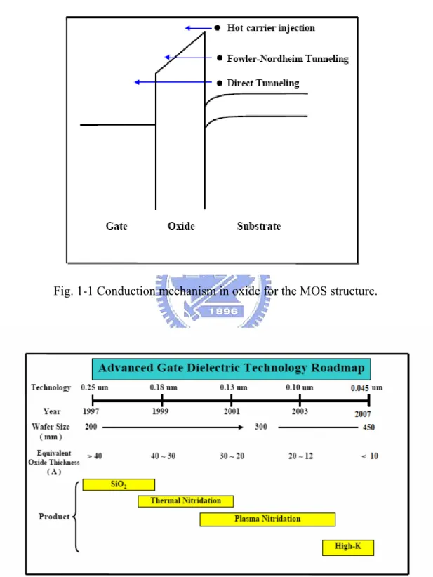
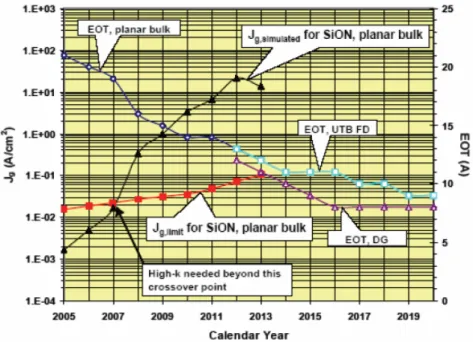
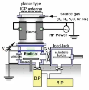
(11) Table Captions Chapter 1. Table 1-1 High-performance Logic Technology Requirements Roadmap. ( ITRS:2006 updae )…………………………………………………….41 Table 1-2 Characteristics of various high-k materials……………………………….42. Figure Captions Chapter 1. Fig. 1-1. Conduction mechanism in oxide for the MOS structure. ………..………43. Fig. 1-2. Roadmap of the gate dielectric. ……………….…………………..……..43. Fig. 1-3. With the marching of technology nodes, gate dielectric has to be shrunk and five silicon atoms thick of gate dielectric is predicted for 2012.[9]….44. Fig. 1-4. Measured and simulated Ig-Vg characteristics under inversion condition for nMOSFETs. The dotted line indicates the 1A/cm2 limit for the leakage current. [10]……………………………………………………………...44. Fig. 1-5. Jg, limit versus Jg, simulated for High-Performance Logic ( ITRS: 2005 update )…………………………………………………….45. Fig. 1-6. Jg,limit versus Jg,simulated for Low Operating Power ( ITRS: 2005 update )…………………………………………………….45. Fig. 1-7. Jg,limit versus Jg,simulated for Low Standby Power ( ITRS: 2005 update ). ……………………………………………………………………………………….46. ix.
(12) Figure-chapter 2. Fig. 2-1. Scaling limits of MOCVD HfO2 and ZrO2 (International SEMATECH Confidential and Supplier Sensitive, 2002)…47. Fig. 2-2. The ICP plasma system that was used in this experiment………………...48. Fig. 2-3 The fabrication flow of the experiment……………………...………..48~50. Figure-chapter 3. Fig. 3-1. The capacitance-voltage (C-V) characteristics of HfO2 gate dielectrics anneal with different temperature for 30 sec from -2 V to 1 V……………51. Fig. 3-2 The J-V characteristics of HfO2 gate dielectrics anneal with different temperature for 30 sec from 0 V to -2 V…………………………………..51 Fig. 3-3. The capacitance-voltage (C-V) characteristics of HfO2 gate dielectrics anneal with dielectrics treated with N2 plasma treatment for different process time……………………………….……………………………….52. Fig. 3-4. The capacitance-voltage (C-V) characteristics of HfO2 gate dielectrics treated with NH3 plasma treatment for different process time. ………...…52. Fig. 3-5. The capacitance-voltage (C-V) characteristics of HfO2 gate dielectrics treated with N2O plasma treatment for different process time. ………...…53. Fig. 3-6. The J-V characteristics of p-type HfO2 capacitors treated by N2 plasma with different process time from 0V to -2V. …………………………………...53. x.
(13) Fig. 3-7. The J-V characteristics of p-type HfO2 capacitors treated by NH3 plasma with different process time from 0 V to -2 V. ……..……………………..54. Fig. 3-8. The J-V characteristics of p-type HfO2 capacitors treated by N2O plasma with different process time from 0 V to -2 V. ……………………………54. Fig. 3-9. The capacitance-voltage (C-V) characteristics of HfO2 gate dielectrics treated with N2 plasma treatment for 60sec, NH3 plasma treatment for 90 sec and N2O plasma treatment for 90 sec. ………...……………………...55. Fig. 3-10 The J-V characteristics of HfO2 gate dielectrics treated with N2 plasma treatment for 90 sec, NH3 plasma treatment for 90 sec and N2O plasma treatment for 90 sec………………………………….…………………..55. Fig. 3-11 The capacitance-voltage (C-V) characteristics of HfO2 gate dielectrics treated with the same PDA temperature annealing and different PDA temperature annealing…………………………………………………..56. Fig 3-12 The J-V characteristics of HfO2 gate dielectrics treated with the same PDA temperature annealing and different PDA temperature annealing………56. Fig. 3-13 The capacitance-voltage (C-V) characteristics of HfO2 gate dielectrics after N2 nitridation and 800 ℃, 850 ℃, 900 ℃ 30 sec thermal treatment…………………………………………………………………57. xi.
(14) Fig. 3-14 The J-V characteristics of HfO2 gate dielectrics after N2 nitridation and 800 ℃, 850 ℃, 900 ℃ 30 sec thermal treatment……..………………57. Fig. 3-15 The capacitance-voltage (C-V) characteristics of HfO2 gate dielectrics after NH3 nitridation and 800 ℃, 850 ℃, 900 ℃ 30 sec thermal treatment…………………………………………………………………58. Fig. 3-16 The J-V characteristics of HfO2 gate dielectrics after NH3 nitridation and 800 ℃, 850 ℃, 900 ℃ 30 sec thermal treatment……………………..58. Fig. 3-17 The capacitance-voltage (C-V) characteristics of HfO2 gate dielectrics after N2O nitridation and 800 ℃, 850 ℃, 900 ℃ 30 sec thermal treatment………………………………………………………………….59. Fig. 3-18 The J-V characteristics of HfO2 gate dielectrics after N2O nitridation and 800 ℃, 850 ℃, 900 ℃ 30 sec thermal treatment……………………...59. Figure-chapter 4. Fig. 4-1 The hysteresis of p-type HfO2 gate dielectrics (sputter) without plasma treatment…………………………………………………………………..60. Fig. 4-2 The hysteresis of p-type HfO2 gate dielectrics (MOCVD) without plasma treatment…………………………………………………………………..60 xii.
(15) Fig. 4-3 The hysteresis of p-type HfO2 gate dielectrics (MOCVD) with PDA 600℃-30 sec, N2 nitridation 60sec, PNA 600℃-60 sec and 800℃-30 sec. ………………………………………………..………………………………………61 Fig. 4-4 The hysteresis of p-type HfO2 gate dielectrics (MOCVD) with PDA 600℃-30 sec, NH3 nitridation 90sec, PNA 600℃-60 sec and 800℃-30 sec. …………………………………..……………………………………………………61 Fig. 4-5 The hysteresis of p-type HfO2 gate dielectrics (MOCVD) with PDA 600℃-30 sec, N2O nitridation 90sec, PNA 600℃-60 sec and 800℃-30 sec. ………………………………………………………………………………………..62 Fig. 4-6. The SILC curve of p-type HfO2 gate dielectrics treated with N2 plasma 60sec for PDA 600℃-30 sec and PNA 600℃-60 sec………….………….62. Fig. 4-7. The SILC curve of p-type HfO2 gate dielectrics treated with NH3 plasma 90sec for PDA 600℃-30 sec and PNA 600℃-60 sec………………….….63. Fig. 4-8. The SILC curve of p-type HfO2 gate dielectrics treated with N2O plasma 90sec for PDA 600℃-30 sec and PNA 600℃-60 sec………….………….63. Fig. 4-9 Gate current shift of p-type HfO2 gate dielectrics treated with N2 plasma treatment for the same annealing process during Vg = 3V CVS for 180sec. ......................................................................................................................................64 Fig. 4-10 Gate current shift of p-type HfO2 gate dielectrics treated with NH3 plasma treatment for the same annealing process during Vg = 3V CVS for 180sec. ………………………………………………………………………………………..64 Fig. 4-11 Gate current shift of p-type HfO2 gate dielectrics treated with N2O plasma treatment for the same annealing process during Vg = 3V CVS for 180sec. xiii.
(16) …………………………………………………………………………………….…65 Fig. 4-12 The J-V curve of p-type HfO2 gate dielectrics treated with N2 plasma 60sec for PDA 600℃-30 sec and PNA 600℃-60 sec at 25℃, and 125℃ from -2 V to 0 V…………………………………………………………65. Fig. 4-13 The J-V curve of p-type HfO2 gate dielectrics treated with NH3 plasma 90sec for PDA 600℃-30 sec and PNA 600℃-60 sec at 25℃, and 125℃ from -2 V to 0 V…………………………………………………………66. Fig. 4-14 The J-V curve of p-type HfO2 gate dielectrics treated with N2O plasma 90sec for PDA 600℃-30 sec and PNA 600℃-60 sec at 25℃, and 125℃ from -2 V to 0 V…………………………………………………………66. Fig. 4-15 The J-V curve of p-type HfO2 gate dielectrics treated with N2 60sec ,NH3 90 sec and N2O 90 sec for PDA 600℃-30 sec and PNA 600℃-60 sec at 25℃, and 125℃ from -2 V to 0 V………………………………………67. xiv.
(17) Chapter 1. Introduction. 1.1. Motivation to Study High-k Dielectrics In the scaling of CMOS, reducing the thickness of gate stack with lower leakage. current plays an important role. Although the leakage current of the devices with the same gate dielectric reduces with the scaling gate length and width, that leakage current density increases with the scaling of gate dielectrics exponentially. Therefore, the gate leakage current increases as the device size decreases. The larger leakage current will not only cause the higher power consumption but also degrade the reliability of the devices. [1]-[2] In terms of the first order current-voltage relation, the driving current of a MOSFET can be given as. Where VGS is the applied gate to source, Leff is the effective channel length, W is the channel width, Vt is the threshold voltage, µn is the mobility for electrons, Cg is. 1.
(18) the gate capacitance, κ is the dielectric constant, ε0 is the permittivity of free space and tinv is the electrical film thickness. From the formula, we know that with reduced threshold voltage, smaller effective channel length, and increased gate capacitance as well as gate-to-source voltage, the device can achieve better current driving ability. Of course, it can also have higher device density, which means a better performance and much more transistors on the chip. However, a large VGS will degrade the reliability while too small Vt will result in statistical fluctuation in thermal energy at a typical operation circumstance of up to 100℃. So a bigger Cg and shorter Leff will be needed to maintain device performance. Using the material with high dielectric constant (high-k), the physical thickness of the dielectric in the devices can be increased without the reduction of capacitance density. Since the leakage current is related to the physical thickness, the increasing thickness of high-k dielectric can reduce the leakage current of the devices. Although high k dielectrics often exhibits smaller band gap, weaker bond, and higher defect density than SiO2, the high k dielectrics with the same effective oxide thickness (EOT) with SiO2 still shows lower leakage current than SiO2 by several orders. [3]-[4] That is the reason why high-k dielectrics have drawn much attention for future gate dielectrics. According to the ITRS (International Technology Roadmap for Semiconductor) of SIA as shown in Fig. 1-1 [5]-[6], the thickness of gate oxide have to be below 10 Å after 2007. Moreover, the gate length and bias voltage reduces by 11 % every year while the drive current has to be maintained. Therefore, the continual scaling of gate dielectric is an inevitable trend in proceeding CMOS technology. However, the operation frequency of the device below the generation of 100 nm will be over GHz [7] and the electrical characteristic of high-k dielectrics at that frequency plays an important role for the use of high-speed devices. Even some high -k dielectrics show good electrical characteristics at low frequency, the performance 2.
(19) of those at RF region could possibly degrade. Therefore, it is important to find out the high k dielectric that exhibits superior characteristics at both high and low frequency. Recently, some high-k dielectrics have been widely studied and the characteristics and issues of those materials have also been reported. The high-k dielectrics show good performances are always accompanied by another drawbacks. Finding out the most suitable high-k dielectric for the use of device and altering the device structure or process to meet the requirement of the high-speed device are significant tasks to implant high-k dielectrics to the next VLSI generation.. 1.2 Scaling of the Gate Oxide Thickness The scaling down of the device dimension is an inevitable tendency with each new generation in semiconductor industry. It can increase the output of the product and reduce the cost. The MOS device plays a very important role in the development of the integrated circuit. It largely applies in the commercial products such as dynamic random access memory (DRAM) . [8]. The major factors of the MOS devices, which extensively apply on integrated circuit, are the stability and high efficient electrical characteristics. The characteristics of the MOS device are dominantly affected by the quality of the insulator layer. Then the quality of the insulator layer will be major concern. Current trends in MOS technology are towards higher chip packing density, more complex devices with more process levels, and larger substrate. Development of high-density MOS dynamic random access memory (DRAM) devices with small cell areas has been accomplished by reducing the thickness of the SiO2 storage capacitors to maintain the required charge storage level. But the shrinkage of the oxide thickness causes the increase of the direct tunneling through the gate dielectric and degrades gate oxide reliability with 3.
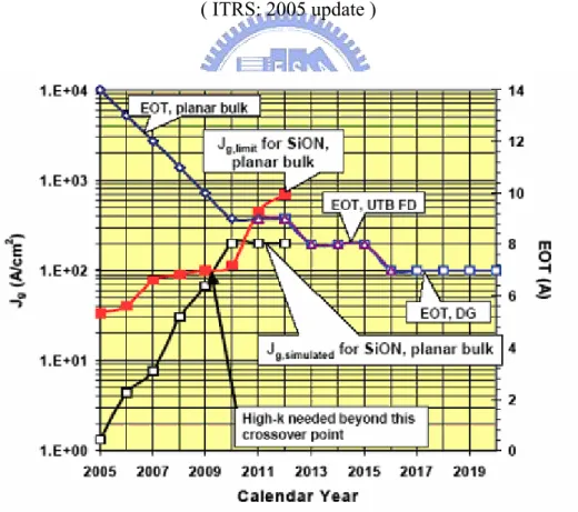
(20) nonlinear scaling of the power supply because of a higher electric field across the gate oxide. Figure 1.1 shows the possible conduction mechanism of the leakage current passing through the oxide. As can be seem from this figure, the probability of the direct tunneling process occurrence is in proportion to the oxide thickness.. 1.3 Roadmap of the Gate Dielectric Figure 1.2 shows the roadmap of the advance gate dielectric in the future. For the 0.18 um technology the material used to act as the gate dielectric still is silicon dioxide ( SiO2 ) with a thickness lower than 4 nm. For the next generation, the equivalent oxide thickness decreases to below 3 nm. Then the conduction of the leakage. current. passing. through. the. silicon. dioxide. changes. from. the. Fowler-Nordheim tunneling to the direct tunneling. Then the direct tunneling leakage current can be many orders-of-magnitude larger than F-N tunneling leakage current. For suppressing the leakage current the increase of the physical thickness of the gate dielectric with still keeping the same equivalent oxide thickness seems to be a good method. It means that the gate dielectric must have higher relative dielectric constant than that of the pure silicon dioxide. If people still want to use the silicon dioxide as the base of the gate dielectric, the nitridation of the silicon dioxide seems to be a good method. Then the silicon oxynitride ( SiOxNy ) will possess higher relative dielectric constant than silicon dioxide. For the next generation, the staked nitride ( Si3N4/SiO2 ) will be the appropriate candidate to conform to the requirement of leakage current suppression. When the equivalent oxide thickness decrease to about 1.2 nm, the material with the high relative dielectric constant (high-k) will be the only choice. In this thesis, the researches are mainly divided into two sections. First section is focus on the improvement of the oxide quality. For fitting in with the future requirement,. 4.
(21) the second section is researching the material with high relative dielectric constant to substitute for the silicon dioxide.. 1.4 The Need to Use High-k Materials 1.4.1 Motivation to Study High-k Dielectrics Over the past 30 years, SiO2 has served its role as a perfect gate dielectric, and has been scaled down from a thickness of 100nm to 1.2nm at 90nm process technology node today, in order to gain a large Cg and a higher density. In 1999, Schulz in Nature predicted that, in order to keep up with the roadmap goal, in 2012 the thickness of gate oxide is slated to scale down to 1nm, which represents only five silicon atoms thick ( see Fig 1-3 ) [9]. Thus the direct tunneling current which depends strongly on film physical thickness will increase to an unacceptable range, resulting in a high power dissipation and heat .we can see the machine from(1.3).. We can see from Fig. 1-4, Lo et al. find that the gate oxide can be scaled down to 2nm before exceeding the limit of 1A/cm2 from the viewpoint of allowable stand-by power dissipation. Below 2nm, however, the oxide tunneling current will quickly becomes problematic. For easily sensing the seriousness of leakage problem: as SiO2 thickness is reduced, leakage current increases exponentially (~10×/2Å)[10] On the other hand, we can take the view of Roadmap of gate dielectric. Fig. 1-5. 5.
(22) shows the high-performance logic scaling-up of gate leakage current density limit and of simulated gate leakage due to direct tunneling. In 2006, the EOT ( Effective Oxide Thickness ) is about 1.1 nm and the leakage current density of the oxynitride is below the leakage limit line. However, after 2008, the EOT is below 1.0 nm and the oxynitride is incapable of meeting the limit on the gate leakage current density. Fig. 1-6 shows the low operating power (LOP) scaling-up of gate leakage current density limit and simulated gate leakage due to direct tunneling. In 2006, the EOT is only 1.3 nm but the leakage current density of the oxynitride is still below the limit line because the application of high-performance logic could endure larger gate leakage current. However, after 2010, the oxynitride couldn’t be used for high-performance logic anymore. Fig. 1-7 shows the Low Standby Power scaling-up of gate leakage current density limit and simulated gate leakage due to direct tunneling. About this case we can notice that the oxynitride couldn’t be used for Low Standby Power device anymore after 2007. Table 1-1 is the roadmap of 2006 ITRS update. (International. Technology. Roadmap. for. Semiconductor). for. the. high-performance logic technology. After 2008, the requirement of EOT even reduces to less than 1 nm. It would be a big challenge because the leakage current is too large to be acceptable for SiO2 under such a thin thickness Because the leakage current is related to the physical thickness of the gate oxide from (1.3), we can notice that if we make the gate dielectric thicker and still maintain the same Cg value, the leakage current problem would be solved. This is mean that there will be a new material to replace traditional SiO2 gate dielectric. In order to maintain the same Cg value, (1.2) can be rewritten as follows:. 6.
(23) where the teq term represents the theoretical thickness of SiO2. So by increasing the gate dielectric constant, the same equivalent oxide thickness can be obtained with a thicker physical thickness, which can reduce the gate leakage current (i.e., direct tunneling), without sacrificing the performance. Consequently, SiO2 gate dielectric needs to be replaced by the material with high dielectric constant.. 1.4.2 The advantages of High-k dielectric High-k gate materials can maintain the same EOT with thicker physical thickness, and is therefore expected drastically reduced direct-tunneling current. From Fig1-8, the increased physical thickness significant reduces the probability of tunneling across the insulator, and hence, reduces the amount of off-state leakage current density. [11] The relationship between dielectrics constant and thickness is followed:. A suitable replacement gate dielectric with a high permittivity (k) must exhibit low leakage current, have the ability to be integrated into a CMOS process flow, and exhibit at least the same equivalent capacitance, performance, and reliability of SiO2.. 7.
(24) 1.4.3 The choice of High-k materials There are many potential candidates for replacing SiO2, such as HfO2, ZrO2, Al2O3, Ta2O5 and so on. Which one will emerge as the winner for replacing the silicon dioxide? Since over the past three decades, SiO2 has served as an ideal gate dielectric, its several advantages, such as being amorphous phase through the whole integration processing, high quality interface, and good thermal stability, can indeed serve as a good guide of choosing high-k material. So, an ideal gate dielectric should meet the following requirements below:. Physical Properties a. Suitable high k value (12~60) A suitable k value is indispensable. Those with not enough high-k value could not satisfy (1.3) to lower the leakage by increasing physical thickness. While those with too high-k value, in general, would suffer from thermal stability issues and larger fringing field. b. Thermodynamic stability in direct contact with silicon Preserve capacitance of gate stack after processing. c. Wide bandgap with conduction band offset > 1eV It is found that most of the high-k materials do not have wide enough bandgap. In contact with silicon and gate electrode, the bandgap is closely related to the barrier height for carrier transport. Low bandgap will lead to intolerably high gate leakage (leakage current ~exp(-△Ec)) [12]. d. Gate material compatibility Materials such as metal gate, and metals have been considered for better controllability and better performance.. 8.
(25) e. Film morphology (amorphous) and stable process compatibility In the VLSI process, the thermal budget is an important issue since high temperature changes dielectric phase. Once the gate dielectric material has transformed to polycrystalline from amorphous phase, the large grain boundaries would serve as leakage path, and induce large leakage current.. Electrical Properties (a)Low interface state density (Dit< 5x10¹⁰/cm2-eV-1), and SiO2-like mobility, The interface would affect the carrier mobility in the channel, and from (1.2), mobility degradation is related to poor current drivability. In high-k, there are so many sources that would reduce mobility, such as fixed charge, remote phonon, interfacial dipoles, remote surface roughness, surface roughness and phase separation crystallization. And most of them can be avoided by improving process technology. (b) VFB and hysteresis < 20mV, (c) Tinv<1nm, (d) J<10-3A/cm2@ VDD, (e) Reliability issue. (f) No C-V dispersion,. To serve as a new gate dielectric, we must also take into consideration electrical reliabilities, such as stress-induced leakage current (SILC), time dependent dielectric breakdown (TDDB), hot carrier aging, bias temperature instability and charge trapping issues [13].. 9.
(26) 1.4.4 Why choose HfO2 There are many kinds of high-k materials, including Al2O3, Y2O3, Ta2O5, TiO2, ZrO2 and HfO2 etc. Table 1-2 lists basic characteristics of several high-k dielectrics. Unfortunately, many high-k materials such as Ta2O5, TiO2, SrTiO3, and BaSrTiO3 are thermally unstable when directly contacted with silicon [14] and need an additional barrier layer which may add process complexity and impose thickness scaling limit. Also, materials with too low or too high dielectric constant may not be adequate choice for alternative gate dielectric application. Ultra high-K materials such as STO or BST may cause fringing field induced barrier lowering effect [15]. Materials with relatively low dielectric constant such as A12O3 and Y2O3 do not provide sufficient advantages over SiO2 or Si3N4 [16]. Among the medium-k materials compatible with silicon, oxides of Zr and Hf are attracting much attention recently. Especially, Hf forms the most stable oxide with the highest heat of formation (∆Hf = 27l Kcal/mol) among the elements in IVA group of the periodic table (i.e. Ti, Zr, Hf). Unlike other silicides, the silicide of Hf can be easily oxidized [17]. HfO2 possesses a dielectric constant of up to 25 [18], a large bandgap of 5.7 eV with sufficient band offset of larger than 1.5 eV [19], and well thermal stability in contact with silicon [20]. HfO2 is very resistive to impurity diffusion and intermixing at the interface because of it’s high density (9.68 g/cm3) [21]. In addition, HfO2 is the first high-k material showing compatibility with polysilicon gate process [22]. These properties make HfO2 to be one of the most promising candidates for alternative gate dielectric application. Although inadequate mobility of HfO2 MOSFETs is among the biggest concerns, various techniques have been explored to enhance the mobility. Introduction of strained silicon substrate [23], for example, drastically improved the mobility by changing the band structure of the substrate rather than changing the dielectric itself.. 10.
(27) However, the characteristics and mechanism of HfO2 are not totally understood.. 1.5 Plasma Nitridation According to traditional view of improving SiO2 device performance, we could find that nitridation is a common method to improve the interface. [24] Property with the result that there is often Nit or Dit in the interface, imperfect bonding of interface usually makes the characteristic of the device deteriorate. Such as charge will be trapped by the defects of the interface, it produce flat band voltage shift and also reduce mobility. Another shortcoming is that these dangling bonds will easily bond with oxygen atom in the following high temperature environment. The extra chemical reaction will let the interfacial oxide growth, and it will reduce the C value because of the lower dielectric constant. In addition, the quality of interfacial layer formed by oxidation is worse, and it would cause the problem of charge trapping. In order to solve these problems, nitridation treatment could let the atom of nitrogen bond with these dangling bonds and fix it while entering the interface layer, and then improve the stability and reliability of interface. Consequently, nitridation treatment is a workable solution to improve interface quality. As we note before, the question about using high-K materials to replace SiO2 is that there are too many defects in the interface to cause reliability degradation. Therefore, when we use high-K materials, it is consider that nitridation treatment is a more suitable way to improve reliability and thermal stability of device. These kind of treatment have already used in some relevant references. [25] [26] Among them, someone take nitridation treatment at high temperature, others take so-called plasma nitridation . According to [27], we could understand that the effect of plasma nitridation is better than thermal nitridation. The reason is that high-k materials could not sustain high thermal stress. As long as the temperature reaches certain degree, we would see the phenomenon of crystallization. 11.
(28) The crystallization of dielectric would increase leakage current substantially, because it offers the path of leakage current. On the other hand, the meaning of plasma nitridation is to activate the source gas first. The high activation energy of radical will provide better mend which is better than nitridation at high temperature. For all these reasons, we adopt plasma nitridation in present experience.. 1.6 Thesis Organization Following chapters in the thesis are primarily organized as follow: In chapter 2, we make a description of experimental details. Metal-Organic Deposition system is used to deposit hafnium-based materials on silicon surface. In chapter 3, we discuss the characteristics of HfO2 or insulator by Metal-Insulator-Semiconductor (MIS) capacitors. In chapter 4, we discuss the reliability of HfO2 or insulator by Metal-Insulator-Semiconductor (MIS) capacitors and the effects of Post-Metallization-Annealing. In chapter 5, we make the conclusions for this thesis and provide some suggestions for future work.. 12.
(29) Chapter 2. Experiments of Al/Ti/HfO2/Si MIS Capacitor. 2.1 The methods to prepare High-k thin film There are many methods to prepare high-k thin films, such as chemical vapor deposition (i.e. MOCVD, ALCVD, PECVD etc.) [28]-[30] and physical vapor deposition (i.e. Sputtering, PLD etc.) [31][32]. MOCVD, ALCVD and Sputtering are the typical methods for preparing HfO2 films. We will compare the MOCVD and sputter methods below.. 2.1.1 MOCVD MOCVD (metal-organic CVD) is a widely used technology for depositing a variety of thin films, including metal oxide and metal silicate films, for high-k gate dielectric applications. The basic steps in MOCVD deposition method are as follows: 1. MO precursor in company with N2 process gas and O2 process gas are injected into the reactor. 2. The sources are mixed inside the reactor and transferred to the deposition process chamber. 3. At the deposition process chamber, high temperature results in the decomposition of sources and other gas-phase reactions, forming the film precursors that are useful for film growth and byproducts.. 13.
(30) 4. The film precursors transport to the growth surface. 5. The film precursors absorb on the growth surface. 6. The film precursors diffuse to the growth site. 7. At the surface, film atoms incorporate into the growing film through surface reaction. 8. The byproducts of the surface reactions desorb from the surface. 9. The byproducts transport to the main gas flow region away from the deposition area toward the reaction. Then the wafer exits. From fig. 2-1, it is apparent that 1 nm EOT can be achieved with MOCVD metal oxide films when a metal electrode is used. However, most of the devices with MOCVD HfO2 and HfSixOy when a poly-Si gate is used have EOT greater than 2 nm. Unlike metal electrode, using poly-Si electrode requires the high-k gate stack to go through a 1000°C/10 sec S/D activation anneal step. This step not only results in chemical and structural changes in the high-K film, but also affects interfaces between the high-k film/substrate and the high-k/poly-Si electrode. All devices fabricated with MOCVD ZrO2 and ZrSiO films using poly-Si gate electrode were too leaky to give any meaningful C-V results. In general, using poly-Si gate electrode results in around 0.7 to 1 nm higher EOT for gate stacks fabricated with HfO2 and HfSixOy gate dielectric films. This additional interfacial oxide thickness is too large to be acceptable. In view of this, the MOCVD is not a good tool for high-k material deposition with poly-Si gate. However, the MOCVD has very good throughput and can process a 25-wafer lot in ~2 hours (roughly 4X better than ALCVD). Thus, from a throughput perspective, the MOCVD has a distinct advantage over the ALCVD [33].. 14.
(31) 2.1.2 DC Magnetron Sputtering The usual HfO2 film with DC magnetron sputtering method is reactively sputtered from an Hf target in an Ar + O2 ambient onto Si substrate. The advantages of the DC magnetron sputtering are simple and cheap. In addition, the HfO2 film prepared by CVD system easily contains organic impurities and/or oxygen vacancies inside. This will cause leakage current through Frenkel-Pool effect or trap assisted tunneling [34]. Less contaminants are produced by the process of the sputtering because there is no other unnecessary chemicals. However, the uniformity of the DC sputtering is worse than that of the ALCVD and the MOCVD in 12 inch diameter Si wafer. Further, sputtering in an O2 ambient easily produces SiO2 interfacial layer. Therefore, we decide to sputter Hf in an Ar ambient only. After pure Hafnium has been deposited on Si substrate, we put the wafer into furnace system with O2 ambient at some low temperature for oxidation. At some low temperature (<500℃), Si will not react with O2 to form the SiO2. Then, the HfO2 film is prepared without SiO2 interfacial layer.. 2.2 Rapid Thermal Annealing system METAL RTA-AG 610 was a single-wafer lamp-heated and computercontrolled rapid thermal processing (RTP) system. Water and compressed dry air (CDA) cooling system were used to cool down the quartz chamber. High intensity visible radiation heating and cold-heating chamber walls allow fast wafer heating and cooling rate. The tungsten halogen lamps were distinguished into five groups, and the relative percentage of lamp intensity can be adjusted individually for each group to achieve uniform temperature distribution. Temperature was obtained from pyrometer and precise controlled by computer. Two gas lines were used in the system which can 15.
(32) be switched between Ar and N2. Before RTA process started, one minute N2 gas purge was performed to minimize the water vapor introduced during wafer loading and also swept unwanted particles induced during process. A fast heating rate of 100℃/sec was chosen in this work. When anneal was complete, chamber temperature was quickly cooled down from 900℃ to 500℃ by N2 purge 60 seconds. Then, the chamber was slowly cooled down to 280℃ without N2 purge to avoid creaking of films. After five minutes later, wafers can be taken out from the chamber. Films’ creak can be avoided by two-steps-cooling method.. 2.3 Plasma treatment system When the PDA (Post-Deposition-Annealing) was finished, some samples were subjected to an additional plasma treatment in order to improve the electrical properties of gate dielectric. There were various source gas (N2, NH3, N2O) and process time (30 sec, 60 sec, 90 sec, 120 sec) as the experiment conditions. Parallel plate high-density plasma reactor employing an ICP source was a single-wafer treated and computer-controlled system. Fig. 2.2 illustrates ICP system that was used in this experiment. 13.56 MHz RF power was coupled to the top electrode through a matching network. After the sample load to reactor, the system was pumped down to keep the chamber clean enough. Subsequently, the source gas was become radical by the plasma system, as the chamber pressure was 100 mTorr and the substrate temperature was 300℃ so that to achieve the goal of low temperature process. The power of working plasma was kept constant at 200W and the flow rate of source gas was 100 sccm. While the process of plasma treatment was finished, these samples were brought to thermal treatment to. 16.
(33) reduce plasma damage.. 2.4 MIS Capacitors Fabrication Process In this thesis, Al/Ti/HfO2/Si capacitor were fabricated to study ultra thin HfO2 gate dielectrics. Figure 2-3 shows the fabrication flow of this experiment. The starting wafer was four inch <100> orientated p-type wafer. It was one side polished and its resistivity was 5~10 ohm-cm. After standard initial RCA cleaning, wafers were put into chamber and grew HfO2 layer with atomic layer deposition system. After the thin films were prepared, some samples were annealed after deposition (post-deposition anneal) and then subjected to an additional plasma treatment at the substrate temperature of 300℃ while the pressure was 100 mTorr and the plasma power was 200W. The plasma treatment conditions were in pure N2 , NH3 and N2O for 30 sec, 60 sec, 90 sec and 120 sec respectively and the flow rate were 100 sccm. After nitridation, we also annealed these samples to reduce the plasma damage. Finally, pure aluminum films were thermally evaporated on the top side of wafers. Mask defined the top electrode. Then, we used wet etching to etch undefined Al and HfO2 films. After patterning, backside native oxide was stripped with diluted HF solution, and Al was deposited as bottom electrode. The detailed fabrication process flow was listed as follows.. 1. Initial RCA cleaning.. 2. MOCVD(metal-organic CVD) deposition 60Å HfO2 thin film.. 3. Post-deposition anneal with 600℃ for HfO2.. 17.
(34) 4. Plasma treatment with N2,NH3,N2O plasma for 30 sec, 60 sec, 90 sec, 120 sec respectively.. 5. Post-nitridation annealing with 600℃-30sec.. 6. Thermally evaporate 400 Å titanium above the HfO2 films.. 7. Thermally evaporate 4000 Å aluminum as the top electrode.. 8. Mask: define top electrode and then wet etch undefined Ti,Al and HfO2 films.. 9. Strip backside native oxide and coat 4000 Å aluminum as bottom electrode.. After the Al/ Ti/ HfO2 /Si MIS capacitors were prepared, we used semiconductor parameter analyzer (HP4156A) and C-V measurement (HP4284) to analysis electric characteristics (i.e. I-V, C-V, EOT, leakage current density etc.). Then we tested their reliability, including stress induced leakage current (SILC), constant current stress(CCS), constant voltage stress (CVS), Hysteresis effect.. 18.
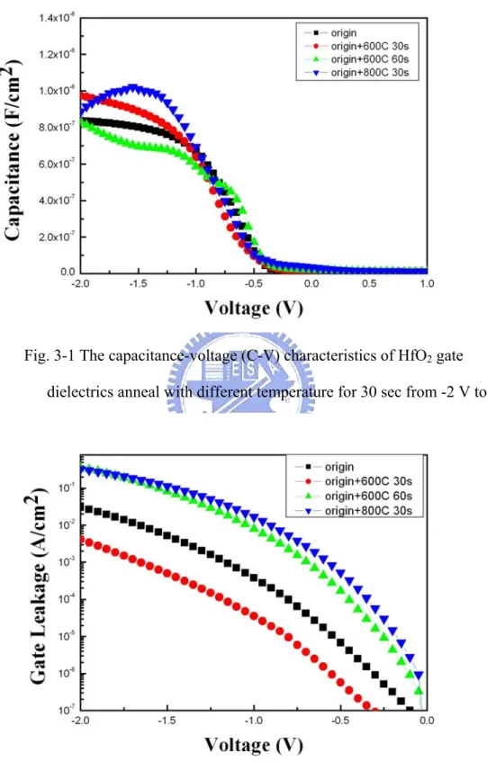
(35) Chapter 3 Electrical Characteristics of Al/Ti/HfO2 MIS Capacitors. 3.1 Electrical Characteristics with different post-deposition annealing (PDA) temperature 3.1.1 Capacitance-Voltage Characteristics for HfO2 In order to measure the C-V characteristics of our MIS capacitors, we used HP 4284A precision LCR meter in our experiments. We swept the gate bias from accumulation region to inversion region to obtain the curve at the frequency of 50 kHz from -2V to 1V. There are three kinds of plasma treatment with different source gas ( i.e. N2, NH3 and N2O ) and they were treated for different process time ( i.e. 30 sec, 60sec, 90sec, and 120sec). Primarily, the effects of different PDA (post deposition annealing) will be discussed. Fig. 3-1 exhibits the capacitance-voltage (C-V) characteristics of HfO2 gate dielectric anneal with different temperature for 30 sec. The capacitors of PDA (600℃, 800℃) show higher capacitance than the original sample. In addition, the capacitor of PDA (800℃) exhibits the worse C-V curve, because HfO2 could not sustain the high temperature anneal over 600℃. The best PDA temperature is about 600℃.. 3.1.2 Current-Voltage Characteristics for HfO2 The leakage current of our MIS capacitors were analyzed from the current -voltage (I-V) characteristics measured by an HP4156A semiconductor parameter 19.
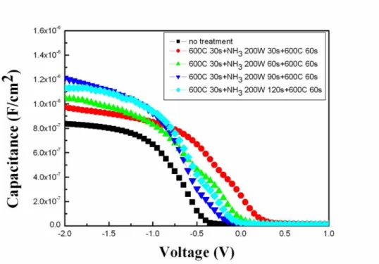
(36) analyzer. Fig. 3-2 exhibits the J-V characteristics of HfO2 gate dielectrics anneal with different temperature for 30 sec from 0V to -2V. We observed that with suitable temperature annealing, the leakage current density can be decreased, because PDA could make the thin film dense. The leakage current density of the sample (PDA-800℃) is larger owing to the crystallization-induced leakage current.. .. 3.2 Electrical Characteristics with different plasma treatment for different process time There are three kinds of plasma treatment with different source gas (i.e. N2, NH3, N2O) and they were treated for different process time (i.e. 30 sec, 60 sec, 90 sec and 120 sec). First, the relationship of difference process time in one kind of plasma treatment will be discussed. Then we compare the effect of different source gas.. 3.2.1 Capacitance-Voltage Characteristics for HfO2 Fig 3-3 shows the capacitance-voltage (C-V) characteristics of HfO2 gate dielectrics treated with N2 plasma treatment for different process time. The capacitor treated for 60 sec shows the maximum capacitance among these conditions of process time. Furthermore, the capacitor treated for 60 sec and 90 sec both show the good capacitance values which are larger than the capacitor which was not treated by N2 plasma. Fig. 3-4 shows the capacitance-voltage (C-V) characteristics of HfO2 gate dielectrics treated with NH3 plasma treatment for different process time. Just like the 20.
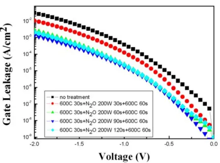
(37) samples of NH3 plasma treatment. The improvement of capacitance could be seen. At this condition, the capacitance treated with NH3 plasma for 90 sec shows the largest value. By the way, all the samples which use NH3 plasma have larger capacitance than the sample without treatment. It is indicated that NH3 plasma treatment is also a practicable method to improve the capacitance-voltage characteristics of HfO2 gate dielectrics.. Fig. 3-5 shows the capacitance-voltage (C-V) characteristics of HfO2 gate dielectrics treated with N2O plasma treatment for different process time. Just like the samples of N2 plasma treatment. The improvement of capacitance could be seen. At this condition, the capacitance treated with N2O plasma for 90 sec shows the largest value. By the way, all the samples which use N2O plasma have larger capacitance than the sample without treatment. It is indicated that N2O plasma treatment is also a practicable method to improve the capacitance-voltage characteristics of HfO2 gate dielectrics.. 3.2.2 Current-Voltage Characteristics for HfO2 Fig. 3-6 shows the J-V characteristics of p-type HfO2 capacitors treated by N2 plasma with different process time from 0 V to -2 V. We observed that the gate leakage current density is suppressed while treatment conditions are 60 sec and 120 sec. It is indicated that N2 plasma treatment supply an effective barrier against the leakage current. The film after N2 plasma treatment became dense and strong, so the leakage current could be effectively decreased, especially for capacitor which treated with N2 plasma 60 sec and it also has the lowest leakage and largest capacitance value from Fig. 3-3. Gate leakage current density of no treatment insulator at VG = -1 V is. 21.
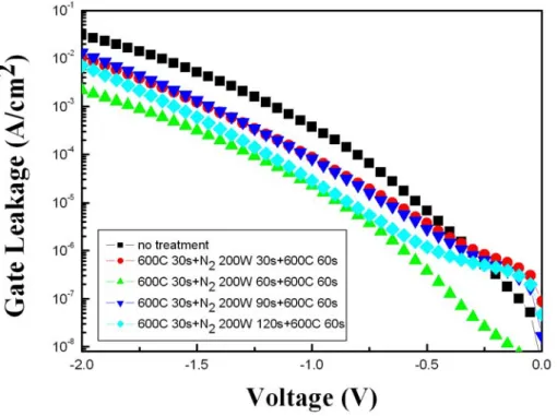
(38) about 1×10⁻⁵ A/cm2. From Fig.3-3, however, gate leakage current density of the capacitor treated for 60 sec N2 plasma at VG = -1 V is about 1×10⁻⁵ A/cm2. It has less gate leakage than no treatment insulator about 1 order. Furthermore, we notices that the capacitor treated with N2 plasma for 30 sec has high leakage current, it is might be that the N2 plasma is too little time to react with the film and caused by plasma damage. Fig. 3-7 shows the J-V characteristics of p-type HfO2 capacitors treated by NH3 plasma with different process time from 0V to -2V. After NH3 plasma treatment, we could see the reduction of leakage current in contrast of no treatment samples. However, the sample of plasma treated for 90 sec got the small gate leakage current and a good C-V curve from Fig 3-4. Relative to the case of N2 plasma, we could see that the level of leakage current increasing obviously mitigate. It is possibly due to the additional oxidation layer formed by oxygen radical. The interfacial oxidation layer will let the dielectric thicker to prevent from gate leakage. Fig. 3-8 shows the J-V characteristics of p-type HfO2 capacitors treated by N2O plasma with different process time from 0V to -2V. After N2O plasma treatment, we could see the reduction of leakage current in contrast of no treatment samples. However, the sample of plasma treated for 90 sec got the small gate leakage current and a good C-V curve from Fig 3-5. Relative to the case of N2 plasma, we could see that the level of leakage current increasing obviously mitigate. It is possibly due to the additional oxidation layer formed by oxygen radical. The interfacial oxidation layer will let the dielectric thicker to prevent from gate leakage.. Fig.3-9 and Fig.3-10 shows the capacitance-voltage (C-V) and J-V characteristics of HfO2 gate dielectrics treated with N2 plasma treatment for 60 sec, NH3 plasma treatment for 90 sec and N2O plasma treatment for 90 sec. It is indicated 22.
(39) that the capacitance treated with NH3 plasma treatment for 90 sec shows the most excellent value (i.e. 42% increasing about capacitance). Among these samples, the reason why the sample treated with N2O plasma has lower capacitance than N2 plasma treatment is complex. It is may be the growing of interfacial oxide made the capacitance value smaller and this interfacial layer also made the gate leakage current smaller.. 3.3 Electrical Characteristics with different steps for PDA and post-plasma treatment anneal. 3.3.1 Capacitance-Voltage and Current-Voltage Characteristics for HfO2 Fig 3-11, Fig 3-12 shows the the C-V and J-V characteristics of HfO2 gate dielectrics treated with the same PDA temperature annealing and different PDA temperature annealing. As show in Fig. 3-11, the sample without nitridation can not sustain the high temperature annealing, so nitridation can improve the thermal stability of high-k film. In addition, we observe that the C-V curve of the sample without PDA and treated by N2 plasma directly is distorted at high negative bias voltages owing to the crystallization, we could see that after post deposition anneal, nitridation could effectively improve the thermal stability of the thin film. From Fig. 3-12, we can find the same result, the sample with nitridation after PDA can effectively decrease gate leakage current. It is good evidence to show that the thin 23.
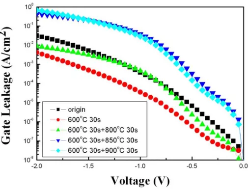
(40) film treated by N2 plasma after post-deposition anneal can make the thin film sustain high thermal stress. The sample with PDA 600℃ 30sec and PNA 600℃ 60sec has the better C-V curve and lower leakage current. Fig 3-13, Fig 3-14 shows the capacitance-voltage (C-V) and J-V characteristics of HfO2 gate dielectrics after the same PDA temperature and the same PNA temperature. After N2 plasma nitridation and 800℃, 850℃, 900℃ 30 sec thermal treatment. We can find the better C-V curve and lower leakage current. The best condition is “PDA 600℃ 30sec + N2 plasma treatment + PNA 600℃ 60sec + 800℃ 30 sec thermal treatment.” Fig 3-15, Fig 3-16 shows the capacitance-voltage (C-V) and J-V characteristics of HfO2 gate dielectrics after NH3 plasma nitridation and 800℃, 850℃, 900℃ 30 sec thermal treatment. The capacitor with PDA 600℃ and after plasma treatment annealing 600℃ certainly has the better C-V curve and lower leakage current. But, the capacitance value decreased at negative bias, this was caused by the additional interfacial layer during the thermal process. However, it is particularly noteworthy that nitridatuon can let the HfO2 gate dielectric sustain high temperature (800℃) thermal treatment. The best condition is “PDA 600℃ 30sec + NH3 plasma treatment + PNA 600℃ 60sec + 800℃ 30 sec thermal treatment.” Compare to Fig 3-1, the film without nitridation will breakdown after high temperature (over 800℃) thermal treatment. Fig 3-17, Fig 3-18 shows the capacitance-voltage (C-V) and J-V characteristics of HfO2 gate dielectrics after N2O plasma nitridation and 800℃, 850℃, 900℃ 30 sec thermal treatment. The capacitor with PDA 600℃ and after plasma treatment annealing 600℃ certainly has the better C-V curve and lower leakage current. But, the capacitance value decreased at negative bias, this was caused by the additional interfacial layer during the thermal process. However, it is particularly noteworthy 24.
(41) that nitridatuon can let the HfO2 gate dielectric sustain high temperature (800℃) thermal treatment. The best condition is “PDA 600℃ 30sec + N2O plasma treatment + PNA 600℃ 60sec + 800℃ 30 sec thermal treatment.” Compare to Fig 3-1, the film without nitridation will breakdown after high temperature (over 800℃) thermal treatment.. 25.
(42) Chapter 4. Reliability of Al /Ti /HfO2 /Si MIS Capacitors. 4.1 Hysteresis When a ferromagnetic material is magnetized in one direction, it will not relax back to zero magnetization when the applied magnetizing field is removed. It must be driven back to zero by the additional opposite direction magnetic field. If an alternating magnetic field is applied to the material, its magnetization will trace out a loop called a hysteresis loop. The lack of retrace ability of the magnetization curve is the property called hysteresis and it is related to the existence of magnetic domains in the material. Once the magnetic domains are reoriented, it takes some energy to turn them back again [38]. The hysteresis phenomenon is similar in the C-V curve of the MIS capacitor device. When we apply a voltage in opposite direction, it will not fit the original C-V curve measured previously. It is due to the traps of interface which would trap charges to influence the flat band voltage and C-V curve. [39] Fig. 4-1 shows the hysteresis of p-type HfO2 gate dielectric which was deposited by sputter system without plasma treatment. Fig. 4-2 shows the hysteresis of p-type HfO2 gate dielectric which was deposited by metal-organic deposition system without plasma treatment. We see that, the hysteresis of the thin film deposited by MOCVD is smaller than the thin film deposited by sputter system. It is a good way to use MOCVD to deposit HfO2 dielectric, because its interfacial trap density is smaller than 26.
(43) the sample deposited by sputter system. Fig. 4-3 shows the hysteresis of p-type HfO2 gate dielectrics (MOCVD) with PDA 600℃-30 sec、 N2 plasma treatment 60 sec 、PNA 600℃-60 sec and 800℃-30 sec. The hysteresis is also small after 800℃ annealing, so nitridation could decrease the trap density and let the thin film sustain high thermal stress. Fig. 4-4 shows the hysteresis of p-type HfO2 gate dielectrics (MOCVD) with PDA 600℃-30 sec、 NH3 plasma treatment 90 sec 、PNA 600℃-60 sec and 800℃ -30 sec. The hysteresis is also small after 800℃ annealing, so nitridation could decrease the trap density and let the thin film sustain high thermal stress. Fig. 4-5 shows the hysteresis of p-type HfO2 gate dielectrics (MOCVD) with PDA 600℃-30 sec、 N2O plasma treatment 90 sec 、PNA 600℃-60 sec and 800℃ -30 sec. The hysteresis is also small after 800℃ annealing, so nitridation could decrease the trap density and let the thin film sustain high thermal stress. As a consequence, the plasma treatment can improve the reliability of gate oxide. The limit of hysteresis for transistor in the future generation is about 10 mV or less than it under high frequency C-V measurement. It seems we could use metal-organic deposition to deposit the HfO2 thin film to decrease hysteresis of HfO2 device.. 4.2 Stress Induced Leakage Current (SILC) In order to investigate the reliability of MIS capacitor device, the stress induced leakage current (SILC) is a common and simple experiment. The additional stress would induced trap density in the bulk or interfacial layer. The trap density would introduce another leakage path. Fig. 4-6 shows the SILC curve of p-type HfO2 gate dielectrics treated with N2 plasma for PDA 600℃-30 sec and PNA 600℃-60 sec.. 27.
(44) First, we used constant voltage (2V) for 60 sec, but SILC did not increase. Therefore, we use constant voltage (3V) for 180 sec to stress the thin film. After the stress of constant voltage (3V) for 180 sec, the gate leakage current become larger then before. The degree of leakage current degradation can be judged for the reliability of MIS capacitor. From Fig. 4-6, it shows the film after high temperature treatment, the quality would become worse, but it was better than the sample without nitridation. Second, it is considered that the SILC of sample (600 ℃-30 sec + N2 plasma treatment 60 sec + 600℃-60 sec + 800℃-30 sec) which has the best C-V curve and the lowest leakage shows a small degradation. On the other hand, it is also can be noticed that the SILC of other samples is large. Fig. 4-7 display the SILC curve of p-type HfO2 gate dielectrics treated with NH3 plasma treatment for PDA 600℃-30 sec and PNA 600℃-60 sec. First,we use constant voltage (2V) for 60 sec to stress the thin film, but we found that the thin film could not sustain the gate voltage stress, the SILC of all the samples were very large, so we use (3V) for 180 sec to replace the original ones. In Fig. 4-7, it was indicated that the SILC of the sample (600 ℃- 30 sec + NH3 plasma treatment 90sec+ 600℃ -60 sec + 800℃- 30 sec) was the smallest. The leakage current of other samples after stress were larger than original ones. So, nitridation can decrease the SILC degradation effectively. Fig. 4-8 display the SILC curve of p-type HfO2 gate dielectrics treated with N2O plasma treatment for PDA 600℃-30 sec and PNA 600℃-60 sec. First,we use constant voltage (2V) for 60 sec to stress the thin film, but we found that the thin film could not sustain the gate voltage stress, the SILC of all the samples were very large, so we use (3V) for 180 sec to replace the original ones. In Fig. 4-8, it was indicated that the SILC of the sample (600 ℃- 30 sec + N2O plasma treatment 90sec+ 600℃ -60 sec + 800℃- 30 sec) was the smallest. The leakage current of other samples after 28.
(45) stress were larger than original ones. So, nitridation can decrease the SILC degradation effectively.. 4.3 Constant Voltage Stress (CVS) To study the reliability of thin films, we can stress the samples with a constant voltage or a constant current, which are useful methods. The mechanism of CVS is the charge trapped by the interfacial trap density which is caused by stress for a long time. In addition, the increasing interface trap density would cause new leakage path to add leakage current. In our experiments, we use constant voltage stress (CVS) to test the reliability of the thin film. Fig. 4-9 shows gate current shift of p-type HfO2 gate dielectrics treated with N2 plasma treatment 60 sec for different annealing process during CVS with Vg = 3 V. It indicated that the thin film with N2 plasma treatment 60 sec which current shift was smaller than the original one. The sample with N2 plasma treatment 60 sec after the 800℃ annealing also had smaller current shift. Fig. 4-10 shows gate current shift of p-type HfO2 gate dielectrics treated with NH3 plasma treatment 90 sec for different annealing process during CVS with Vg = 3 V. It indicated that the thin film with NH3 plasma treatment 90 sec which current shift was smaller than the original one. The sample with NH3 plasma treatment 90 sec after the 800℃ annealing also had smaller current shift.. Fig. 4-11 shows gate current shift of p-type HfO2 gate dielectrics treated with N2O plasma treatment 90 sec for different annealing process during CVS with Vg = 3 V. It indicated that the thin film with N2O plasma treatment 90 sec which current shift was smaller than the original one. The sample with N2O plasma treatment 90 sec after. 29.
(46) the 800℃ annealing also had smaller current shift. It had similar behavior like the previous experiment. The gate leakage shift level of the samples with or not nitridation different about 2 orders, so nitridation process could decrease the trap density effectively. It might be a good way to incorporate N atoms in the thin film to improve the reliability of the gate dielectrics.. 4.4 Measured at High Temperature As shown in fig 4-12 shows J-V characteristics of p-type HfO2 with origin sample, origin + 600℃ 30 sec + N2 200W 60 sec + 600℃ 30 sec two condition measured at 25℃, and 125℃ from -2 V to 0 V. At higher measurement temperature, HfO2 capacitor has larger gate leakage current due to the higher energy of electrons. Besides, gate leakage current at VG = -1V has smaller increase from 25℃ than from 125℃. This hints that gate leakage current becomes to saturate at high measurement temperature. Fig 4-13 shows J-V characteristics of p-type HfO2 with origin sample, origin + 600℃ 30 sec + NH3 200W 90 sec + 600℃ 30 sec two condition measured at 25℃, and 125℃ from -2 V to 0 V. At higher measurement temperature, HfO2 capacitor has larger gate leakage current due to the higher energy of electrons. Besides, gate leakage current at VG = -1V has smaller increase from 25℃ than from 125℃. Fig 4-14 shows J-V characteristics of p-type HfO2 with origin sample, origin + 600℃ 30sec + N2O 200W 90sec + 600℃ 30s two condition measured at 25℃, and 125℃ from -2 V to 0 V. At higher measurement temperature, HfO2 capacitor has larger gate leakage current due to the higher energy of electrons. Besides, gate leakage current at VG = -1V has smaller increase from 25℃ than from 125℃. Fig 4-14 shows J-V characteristics of p-type HfO2 with N2 60sec ,NH3 90 sec. 30.
(47) and N2O 90 sec for the same annealing process time and temperature for two condition measured at 25℃, and 125℃ from -2 V to 0 V. This hints that gate leakage current becomes to saturate at high measurement temperature. This hints that gate leakage current becomes to saturate at high measurement temperature. We find that HfO2 capacitor generates breakdown more easily at higher measurement temperature. This is attributed to electrons have higher energy at higher temperature and result in harder damage in HfO2 film.. 31.
(48) Chapter 5. Conclusions and Future work. 5.1 Conclusions In this thesis, characteristics and reliability of HfO2 gate dielectrics with the post-deposition annealing (PDA) and the post plasma treatment (PNA) have been investigated. These methods could be improved that the quality of HfO2 thin film. The plasma treatment conditions are N2, NH3 and N2O plasma for 30 sec, 60 sec, 90 sec and 120 sec individually. After the post-deposition annealing (PDA), the plasma treatment and the post plasma treatment (PNA), our experimental data revealed low leakage current density and good thermal stability. We find several important phenomena and they would be summarized as follows. First, improvement in the electrical characteristics of Al/Ti/ HfO2 /Si MIS capacitors after post-deposition-annealing has been demonstrated in this work. The HfO2 thin film after PDA would become dense and we could find their capacitance would increase and gate leakage current would decrease. Second, all of the samples after plasma treatment can promote the electrical characteristics and reliability until the plasma damage happened. Among these treatments, the sample treated by N2 plasma treatment for 60 sec, NH3 plasma treatment for 90 sec and N2O plasma treatment for 90 sec for HfO2 represented a fairly great improvement, such as good capacitance ( 40% increasing for HfO2 ), reduced leakage current ( about 1.5 order reduction for all samples ). It was showed 32.
數據
+7
相關文件
Third, during period of DPP as ruling party, little evidience shows that connecting with DDP increases dividend, yet there is significance negative relationship between the
Set up the air current one wind speed it change with wind direction,flow for windbreaks during flowing field instead of after building, air current materials to
Several methods that modulation effective work function to maintain p-type gate material is the direction of future research, sush as microwave annealing with plasma
等溫電漿應用於電弧熔鍊(Arc Refinement)、電漿融射(Plasma Spraying)及感應偶合電漿分光儀(Inductively Coupled Plasma Optical
It would be game-changing to form a class atmosphere that encourage diversity and discussion, formed of groups with different microculture that optimized the sense of belonging
記錄在電子課本 P.11。.. 播放「不同物料的傳熱速度」影片,請學生觀察實驗過程及 結果,並記錄在電子課本 P.13 上。.. 10. 課後
In fact, his teachers believe that it is his good ear for music that has helped him with the precise pronunciation of different languages – especially with a tonal language like
• If the car (mobile) is moving toward the direction of the arriving wave, the Doppler shift is positive.. • Different Doppler shifts if different V
