材料科學與工程學系
博 士 論
文
鎳金屬誘發側向結晶複晶矽薄膜電晶體中電特
性、可靠度與均勻性課題之研究
Investigation of Electrical Properties, Reliability and
Uniformity Issues in Metal-Induced Lateral Crystallization
Poly-Si TFTs
性、可靠度與均勻性課題之研究
Investigation of Electrical Properties, Reliability and
Uniformity Issues in Metal-Induced Lateral Crystallization
Poly-Si TFTs
研 究 生 : 張志榜 Student: Chih-Pang Chang
指導教授 : 吳耀銓 博士 Advisor: Dr. YewChung Sermon Wu
國 立 交 通 大 學
材 料 科 學 與 工 程 學 系
博 士 論 文
A Thesis
Submitted to Department of Material Science and Engineering
College of Engineering
National Chiao Tung University
in partial Fulfillment of the Requirements
for the Degree of
Doctor of Philosophy
in Materials Science and Engineering in
July 2009
Hsinchu 30050, Taiwan, ROC
性、可靠度與均勻性課題之研究
學生:張志榜 指導教授:吳耀銓 博士
國立交通大學材料科學與工程研究所
摘要
低溫複晶矽薄膜電晶體用來製作畫素元件與周邊驅動電路已成為發
展主動式平面顯示器的重要技術。本論文主要在於深入討論並製作有關
高性能複晶矽薄膜電晶體的研究,主要分為以下四個部份來探討。
首先,利用固態連續波雷射將非晶矽薄膜再結晶為複晶矽薄膜已成
功製作出高效能的低溫複晶矽薄膜電晶體,但是受限於雷射能量的高斯
分佈而導致元件的均勻性變差。因此,我們在此提出利用鎳金屬誘發側
向結晶的複晶矽薄膜取代傳統的非晶矽薄膜,接著利用不同能量的固態
植後的金屬誘發側向結晶複晶矽薄膜電晶體可獲得較佳的電特性,其主
要原因為氟離子於複晶矽薄膜內可有效的降低缺陷密度,因而獲得較好
的元件特性。除此之外,與傳統的金屬誘發側向結晶技術相較下,氟離
子的佈植也可使得元件在熱載子劣化下具有較好的對抗能力,使元件具
有較佳的可靠度,並且在製作的過程不需額外的熱退火。
經由論文的第二部份的實驗結果得知,利用離子佈植將氟離子植入金
屬誘發側向結晶複晶矽薄膜內可使得元件特性與穩定性獲得改善,但是
此方式在漏電流的方面並沒有獲得改善,其原因有可能為殘留在薄膜的
鎳金屬濃度並沒有改變。因此在論文的第三個部分我們提出利用四氟甲
烷(CF
4)電漿蝕刻金屬誘發側向結晶複晶矽薄膜的表面,經由電漿處理後
的元件也可獲得電性與可靠度的提升,其主要原因為電漿蝕刻表面後可
有效的降低複晶矽薄膜缺陷密度使得元件特性提升,並且有效的產生矽
氟鍵結(Si-F bond)因而改善元件的可靠度。除此之外,隨著電漿蝕刻表面
時間增加,元件在漏電流方面的表現也可獲得改善。
在論文的最後一部份,我們提出一種新的製作複晶矽薄膜電晶體的技
術-"鎳驅入誘發側向結晶",主要利用氟離子佈植的方式撞擊鍍在非
晶矽薄膜表面的鎳金屬,透過圖形的設計形成鎳金屬驅入側向結晶區,
由此方式發現,利用氟離子驅入的過程,可有效抑制退火再結晶時所產
in Metal-Induced Lateral Crystallization Poly-Si TFTs
Student: Chih-Pang Chang Advisor: Dr. YewChung Sermon Wu
Department of Material Science and Engineering
National Chiao Tung University
Abstract
Low-temperature processed polycrystalline silicon thin-film transistors (LTPS TFTs) as
pixel active elements and in peripheral driver circuits has been an important issue in the
development of active matrix flat panel displays (AMFPDs). This dissertation studies a
number of processing techniques for the high performance poly-Si TFTs. The main focus
of this dissertation can be divided into four parts.
Initially, continuous-wave (CW) laser crystallization (CLC) of amorphous Si (α-Si) has
previously been employed to fabricate high-performance low-temperature polycrystalline
silicon (poly-Si) thin-film transistors (TFTs). Unfortunately, their uniformity was poor
because the shape of beam profiles was Gaussian. Therefore, α-Si film was replaced by Ni
MILCLC-TFT is suitable for application in a system on panel.
Next, the effect of fluorine-ion (F+) implantation on the performance of metal-induced
lateral crystallization (MILC) polycrystalline silicon thin film transistors (poly-Si TFTs)
was investigated. It was found that fluorine ions minimize effectively the trap-state density,
leading to superior electrical characteristics such as high field-effect mobility, low
threshold voltage, low subthreshold slope, and high on/off current ratio. F+-implanted
MILC TFTs also possess high immunity against the hot-carrier stress and thereby exhibit
better reliability than that of typical MILC TFTs. Moreover, the manufacturing processes
are simple (without any additional thermal annealing step), and compatible with typical
MILC poly-Si TFT fabrication processes.
As discussed in part of second, fluorine ion (F+) implantation was employed to improve
the electrical performance of MILC TFTs. It was found that fluorine ions effectively
minimize the trap state density, leading to superior electrical characteristics and better
characteristics. Besides, the leakage current was also suppressed with the increase on
etching time. Moreover, CF4 plasma-treated MILC TFTs also possess high immunity
against the hot-carrier stress and thereby exhibit better reliability than that of conventional
MILC TFTs, which is due to the storng Si-F bonds formed in the MILC poly-Si channel
region.
At the last part of the thesis, a new manufacturing method for polycrystalline silicon thin
film transistors (poly-Si TFTs) using Ni drive-in induced laterally crystallization (DILC)
was proposed. The DILC poly-Si was prepared by collision between F ion implantation
and Ni film through the designed pattern into amorphous-Si (α-Si). It was found that the
drive-in by F atoms effectively suppresses the nucleation of solid phase crystallization
grain and reduces trap-state density, and lead to improve electrical characteristics.
Moreover, the manufacturing processes are simple and compatible with MILC TFT
當開始著手論文的這個部份時,即意味著我將完成博士學位,傷感的是也表示我 要離開交大這充滿人情味的地方。在此要感謝這一路上幫助過我的人,若沒有你(妳) 們的幫忙與相挺,想必我的求學生涯必定無法如此順利且變得枯躁乏味。 首先,感謝我的指導教授吳耀銓博士,感謝您在四年前收了我,讓我能進入這充 滿溫馨與歡樂的研究室並且順利拿到博士學位。也感謝您除了在研究方面的細心指導 外,日常生活的關心也是沒有少過,更感謝您在出國開會時除了要照顧我們之外,還 要不厭其煩的修改我的會議報告投影片。在追隨您求學的這個階段讓我清楚明白身為 一個學者應該有的風範與氣度。謝謝您,我的指導教授吳耀銓博士。 另外,要感謝交通大學電子所林鴻志老師,交通大學材料系陳智老師、吳文偉老 師、亮芯科技陳盈佳副總經理、隆達電子趙志偉副理在百忙之中抽空來參加我的博士 論文口試並不吝指導,使我的論文更加的完備。特別要感謝交大電子所林鴻志老師在 元件特性部分的寶貴意見並撥冗指教。也要感謝交大奈米中心的何惟梅小姐,當我從 碩士班的時候就受到妳的照顧,到了博士班時還是常常的麻煩妳,在此我一定要告訴 大家,妳絕對是奈米中心最 nice 的人。此外也感謝中心裡面的徐綉鑾小姐、黃月美 小姐、范秀蘭小姐、黃國華先生、葉雙得先生、胡進章先生、陳聯珠小姐、林聖欽先 生,感謝妳(你)們在奈米中心裡對我的照顧,讓我在做研究的過程中倍感順利。以及 感謝國家奈米元件實驗室在實驗上的幫忙。 在博士班的求學中還要感謝好多一路相挺的好伙伴們,多虧了你們的幫忙,我才 能順利的拿到博士學位。感謝實驗室的胡國仁學長,親切一直是你給我最深的印象,
討論時的幫忙,更是讓我體會到何為貴族生活的寫照。也感謝實驗室的同學鄭季豪(豪 哥),謝謝你在這段期間給予的幫助,也謝謝你在我們出國開會與旅遊時一切的照顧, 並且從你身上我了解到好男人是怎麼一回事,我想這是我ㄧ輩子也沒有辦法達到的境 界。也感謝同學黃秉緯,感謝你在夏威夷時的相互照應。還有感謝也是低調界的林博 文同學,雖然兩年後你就先到業界去發展了,但也多虧了你,我們才有取之不盡用之 不竭的試片。再來要感謝實驗室的一群學弟妹多謝你們的幫忙,讓我能順利的完成口 試,你們包含了已經畢業的林其慶學弟、吳騏廷學弟、徐志偉學弟、邱偉哲(阿球) 學弟、陳奕宏(阿宏)學弟,還有今年同樣要畢業的廖偉志學弟,在此不得不說你真是 實驗室的潮男,我想你可以考慮跟客家一哥鍾承璋(小鍾)一起組個潮男團體,畢竟我 沒看過那麼會流手汗的人,你們一定會成功的,也謝謝你們的幫忙。也感謝實驗室的 學弟許堉程(manson)、錢奐宇(money),你們的加入讓實驗室變的更有活力。另外也 謝謝實驗室的一姊鄭筑文(老闆娘)學妹,謝謝妳在我要搬家時宅配上的幫忙,也祝妳 生意興隆並且榮登富比士富豪排行榜,到時候可別忘了小弟我。也感謝即將完成碩士 學位並且踏入博士生涯的張勝傑(張哥)學弟、張岱民(小捲)學弟,祝你們這對表兄弟 將來也能順利的拿到博士學位。還有感謝實驗室博士班的棟樑們,賴明輝(小卓)學 弟、陳建誌(God)學弟、謝承佑(wahaha)學弟、陳俞中學弟,感謝你們在實驗上的幫 助,實驗室就交給你們繼續維持下去了,相信你們也可以很快的拿到博士學位。也感 謝學妹卓昕如(阿卓)在實驗上的幫忙,從專題生的時候妳就是位認真的學生,實驗室 能夠有妳的加入必定會使得實驗室研究風氣大大提高,當然也感謝離開實驗室的王宜 代學妹、周亮俞學妹,雖然後來你們並沒有留在實驗室,但是你們加入實驗室的時光, 讓我感受到交大不是只有男生而已。還有感謝後來加入實驗室的專題生,胡人立學 弟、邱郁珈學妹、牛振儀學妹,也祝福你們將來升學順利。也感謝 NDL 幫的李美儀、 楊子明、吳鴻佑,恩…還少了個現在需要低調無法寫出來的人,感謝你們在實驗上的
另外還要感謝涂峻豪學長,從我碩士班時就對我照顧有加,不論是在儀器的訓練 上或者是實驗上的建議,都對我具有相當的幫助。也感謝特別林鈺庭學長還有黃建達 學弟,感謝你們除了在雷射儀器上的大力幫忙外,也因為有你們在奈米中心一起打 拼,讓我在裡面也不覺得孤單,雖然你們都早我一步離開這邊,但那段日子是我無法 忘記的。也謝謝交大光電所的吳興華學長,感謝你當初半夜還願意花時間來訓練我儀 器並且在日後也常常關心我實驗上的進展。 還有我的好朋友-家銘、雅禎、莉晴,感謝你們從我大學生涯就對我無微不至的 照顧,讓我能夠一路的順利拿到博士學位,也祝你們一切順利。還有我碩士班的好朋 友-仁椲、品名、美如、珮如、嘉倫、俊慶,感謝你們在畢業後都還不忘記我,常常 的三五相聚讓我倍感窩心。 謝謝我的女友姍玫,感謝妳在日常生活一切的照料並且包容我的壞脾氣,妳的笑 容是我勇往直前的動力,也因為妳一年來的認真苦讀而順利考上交大,讓我完成了與 學妹交往的小小心願,謝謝妳讓我的世界變的更加完美。也感謝姍玫的家人對我的照 顧,謝謝妳們。 最後,最重要的,要謝謝我的家人。父親張慶沛先生、母親陳桂華女士、大哥張 煥彬、二哥張志鵬以及未來的二嫂吳詩婷,感謝你們一路上對我的支持,讓我能夠毫 無後顧之憂的專注於學業上,並且順利的完成拿到博士學位。真的辛苦你們了,你們 是我最大的驕傲。 若是在上述中沒有提及到的恩人們,請務必見諒,並不是我不知道吃水果要拜樹
Abstract (Chinese) ... i
Abstract (English)... iv
Acknowledgment (Chinese) ...vii
Contents... x
List of Figures... xiv
List of Tables ...xvii
Chapter 1 Introduction ... 1
1.1. Overview of low temperature polycrystalline silicon thin-film transistors (TFTs) ... 1
1.2. Low temperature polycrystalline silicon crystallization methods ... 2
1.2.1. Solid phase crystallization (SPC) method ... 3
1.2.2. Excimer laser crystallization (ELC) method ... 4
1.2.3. Continuous-wave laser crystallization (CLC) method ... 7
1.2.4. Ni metal-induced crystallization (MIC) / Ni metal-induced lateral crystallization (MILC) methods ... 9
1.3. Electrical properties of Ni metal-induced lateral crystallization (MILC) thin-film transistors (TFTs) ... 14
1.4. Reliability issue of poly-Si TFTs... 16
1.5. Motivation and organization of this thesis ... 17
Chapter 2 Electrical characteristics and stability of poly-Si TFTs fabricated by continuous-wave laser annealing of metal-induced lateral crystallized silicon films ... 20
2.2.2. MILCLC poly-Si TFTs... 22
2.3. Results and discussion... 23
2.3.1. SEM analysis of CLC poly-Si films... 23
2.3.2. SEM analysis of MILCLC poly-Si films... 26
2.3.3. Electrical properties of CLC and MILCLC TFTs... 29
2.3.4. Uniformity of CLC and MILCLC TFTs... 31
2.4. Conclusion... 33
Chapter 3 Effect of the F+ implantation on the electrical characteristics and reliability of MILC poly-Si TFTs ... 35
3.1. Introduction ... 35
3.2. Experiment procedure... 36
3.3. Results and discussion... 38
3.3.1. Electrical properties of MILC-TFTs with and without F+ implantation 38 3.3.2. SIMS analysis of F+ implantation Poly-Si film ... 42
3.3.3. Influence of F+ implantation on trap-state density ... 43
3.3.4. Reliability of MILC poly-Si with and without F+ implantation ... 48
3.4. Conclusion... 49 Chapter 4 Influence of etching treatment on electrical and reliability of MILC poly-Si
4.3.3. SIMS analysis of CF4 treated poly-Si film ... 59
4.3.4. Density of states before and after CF4 plasma treated... 60
4.3.5. Activation energy before and after CF4 plasma treated... 62
4.3.6. Reliability before and after CF4 plasma treated... 63
4.3.7. AFM analysis before and after CF4 plasma treated... 65
4.4. Conclusion... 66
Chapter 5 Electrical properties and uniformity of poly-Si thin-film transistors using nickel drive-In induced laterally crystallization ... 68
5.1. Introduction ... 68
5.2. Experiment procedure... 70
5.3. Results and discussion... 72
5.3.1. The relation between drive-in dosage and lateral crystallization length 72 5.3.2. Electrical properties of DILC and MILC TFTs ... 73
5.3.3. Influence of nickel drive-in by F+ implantation on trap-state density. 74 5.3.4. Uniformity of DILC and MILC TFTs ... 76
5.4. Conclusion... 78
Chapter 6 Conclusions and future works ... 79
6.1. Conclusions ... 79
6.2. Future works... 82
6.2.1. Fluorine ion implantation into the buffer-oxide layer of MILC TFTs. 82 6.2.2. Nickel drive-in induce crystallization TFTs ... 82
Fig. 1-1 Roadmap of poly-Si TFT technology. [6]...3 Fig. 1-2 Illustration of transformation scenarios during the ELA process.
Correspond to (a) partial melting, (b) completely melting and (c) near-completely melting of the initial Si film. ...6 Fig. 1-3 Solidification of the molten Si film. Resulting in the higher surface
roughness...7 Fig. 1-4 Global variation in NMOS threshold voltage: ELA (left), CLC (right).
(L/W = 5.4μm/20μm, Tox = 30nm, TFT distance = 0.5mm) [15]...8 Fig. 1-5 Global variation in PMOS threshold voltage: ELA (left), CLC (right).
(L/W = 2.7μm/20μm, Tox = 30nm, TFT distance = 0.5mm) [15]...9 Fig. 1-6 Schematic illustration of the Ni-metal induced Crystallization (MIC)
and Ni-metal induced lateral crystallization (MILC) ...10 Fig. 1-7 Schematic representation of favorable precipitate orientations for
long-range growth of epitaxial Si within the plane of the α-Si. ... 11 Fig. 1-8 Schematic equilibrium molar free-energy diagram for NiSi2 in contact
with α-Si ...12 Fig. 1-9 Schematic representation of a possible growth mechanism involoving
the formation of a thin layer of c-Si at the NiSi2/α-Si interface ...13 Fig. 1-10 The band diagram for the leakage current model. (a) Case of weak
electric field. (b) Case of medium electric field. (c) Case of strong electric field. ...16 Fig. 2-1 SEM images of Secco-etched poly-Si grains irradiated by CW laser
with CLC-2.5 W ...24 Fig. 2-2 SEM images of Secco-etched poly-Si grains irradiated by CW laser
Fig. 2-4 SEM images of Secco-etched poly-Si grains irradiated by CW laser with MILCLC-2.5 W...27 Fig. 2-5 SEM images of Secco-etched poly-Si grains irradiated by CW laser
with MILCLC-3.8 W...28 Fig. 2-6 SEM images of Secco-etched poly-Si grains irradiated by CW laser
with MILCLC-5.0 W...28 Fig. 2-7 Typical IDS-VGS transfer characteristics and field-effect motilities of
MILCLC and CLC TFTs (W/L=20 μm/20 μm)...30 Fig. 2-8 Ten TFTs were measured in each case in field-effect mobility and
threshold voltage to investigate the device-to-device variation. ...32 Fig. 3-1 Schematic diagrams of process flow of MILC poly-Si TFTs with and
without F+ implantation. ...38 Fig. 3-2 The transfer characteristics and field-effect mobility of the MILC
poly-Si TFTs with and without F+ implantation. ...40 Fig. 3-3 Output characteristics of the MILC poly-Si TFTs with and without F+
implantation...42 Fig. 3-4 SIMS depth profile of fluorine and nickel in the structure of interface
of MILC poly-Si/buffer oxide film after annealing at 600℃ for 24 hr....43 Fig. 3-5 The trap state densities (Nt) of TFTs. They can be estimated from the
slope of the linear segment of ln [IDS / (VGS-VFB)] vs. 1 / (VGS-VFB)2 at low VDS and high VGS...44 Fig. 3-6 The activation energy (EA) of drain current as a function of gate
Fig. 4-2 Comparison of transfer characteristics of MILC poly-Si TFTs with and without CF4 plasma etching treated...56 Fig. 4-3 ln [IDS / (VGS-VFB)] vs. 1 / (VGS-VFB)2 at low VDS and high VGS for with
and without CF4 plasma etching treatment...58 Fig. 4-4 SIMS depth profile of Nickel for the MILC poly-Si films and fluorine
for the MILC poly-Si films after CF4 plasma etching treatment...60 Fig. 4-5 The density of state (DOS) distribution in the bandgap of the MILC
poly-Si TFTs with and without CF4 plasma etching treatment...61 Fig. 4-6 The activation energy (EA) of the MILC poly-Si TFTs with and without
CF4 plasma etching treatment...63 Fig. 4-7 The on-current degradation versus stress time for the MILC poly-Si
TFTs with and without CF4 plasma etching treatment. ...64 Fig. 4-8 Surface roughness of CF4 plasma treatment poly-Si film by AFM
analysis. ...65 Fig. 5-1 Schematic illustration of DILC poly-Si process: (a) deposition of α-Si
on oxide-coated Si wafer, (b) deposition of cap-oxide, (c) deposition of Ni film, (d) fluorine ions (F+) implantation, (e) removal of unreacted Ni film and cap-oxide layer, (f) and annealing at 590°C for 3 h...71 Fig. 5-2 MILC and DILC growth lengths as function of annealing time...73 Fig. 5-3 Typical IDS-VGS transfer characteristics and filed-effect mobility of
MILC TFTs and DILC TFTs with various F+ dosages. ...74 Fig. 5-4 SIMS depth profile of fluorine in the structure of interface of DILC
TABLE 2-1 Average values of field-effect mobility and threshold voltage of two different structures with standard deviations in parentheses. ...33 TABLE 3-1 Device characteristics of the MILC poly-Si TFTs with and without F+
implantation...41 TABLE 4-1 Device characteristics of the MILC poly-Si TFTs with and without CF4
plasma treated...57 TABLE 5-1 Average values of the field-effect mobility, threshold voltage,
subthreshold slope, on-state current and off-state leakage current of TFTs with standard deviations in parentheses...77
Chapter 1
Introduction
1.1. Overview of low temperature polycrystalline silicon
thin-film transistors (TFTs)
In 1980, high temperature polycrystalline silicon TFTs had been introduced [1]. They
used chemical-vapor deposited poly-Si to achieve good carrier mobility and electrical
characteristics. With mobility around 50 cm2/V-s, these high temperature poly-Si TFTs
were employed gate insulator SiO2 grown thermally at 1050°C. This approach requires a
high strain temperature substrate such as quartz, incompatible with the commercially
available large area non-expensive glass substrate.
Recently, many researchers have developed various techniques for crystallization of α-Si
at low temperature (below 600°C), and then transformation it to poly-Si; the motivation for
pushing up the mobility to be able to integrate drive circuitry [2], [3]. as well as providing
pixel TFTs and more compatible with the glass substrate. In fact, the field effect mobility
of poly-Si TFTs is significantly higher than that of α-Si about two orders of magnitudes.
The higher drive current allows small TFTs dimension to be used as the pixel switching
improved display performance [4].
Unlike MOSFETs, where the active layer is part of the substrate, in the case of TFTs the
active layer needs to be separately formed on the host substrate. The crystallization method
affect the microstructure quality of the resulting poly-Si film, which means that the
performance of poly-Si TFT will be affected by the selection of techniques for the
crystallization of Si films.
A various techniques have been investigated for crystallization of α-Si at low
temperature such as: (1) solid phase crystallization (SPC) (2) excimer laser crystallization
(ELC) (3) continuous-wave laser crystallization (CLC) (4) Ni metal induced/Ni metal
induced lateral crystallization (MIC/MILC). In the following section, we will review the
crystallization method that the above-mentioned.
1.2. Low temperature polycrystalline silicon crystallization
methods
Crystallization of α-Si films has been considered as the most important process step in
usually has larger grain size than that of as-deposited poly-Si. Historically, solid phase
crystallization was the first technology to produce poly-Si films for display applications [5],
followed by laser crystallization. The ultimate goal of the LTPS technology is to integrate
the pixel-driving circuits on the display substrate. Fig. 1-1 shows the anticipated evolution
of poly-Si technology development and its impact on the degree of on-panel integration
[6].
Fig. 1-1 Roadmap of poly-Si TFT technology. [6]
1.2.1. Solid phase crystallization (SPC) method
Deposited α-Si thin films were transformed to poly-Si using SPC method has obtained
better TFT device electrical performance than as-deposited poly-Si films [7]. For the SPC
method, α-Si films are crystallized in a furnace at temperature about 600°C for duration
density exists in poly-Si films. Amorphous Si is a thermodynamically meta-stable phase
possessing a driving force for transformation to polycrystalline phase given a sufficient
energy to overcome the initial energy barrier.
A key factor affecting crystallization is the nucleation rate in the α-Si films. The
nucleation rate is strongly influenced by the selected deposition method and condition [8],
[9]. The structural order/disorder in the α-Si films affects the films to form stable nuclei.
Higher disorder structure increases the energy barrier required to form the Si nuclei; this
concept has been used in the past to increase the grain size of poly-Si films. Ideally, a
small number of fast-growing nuclei are needed to maximize the grain size. However, the
reality of the situation is that the probability that additional nucleation events will occur
within the volume separating growing nuclei increases geometrically with the separation
distance
1.2.2. Excimer laser crystallization (ELC) method
Excimer laser annealing is suitable for fabrication of LTPS TFTs on large area glass
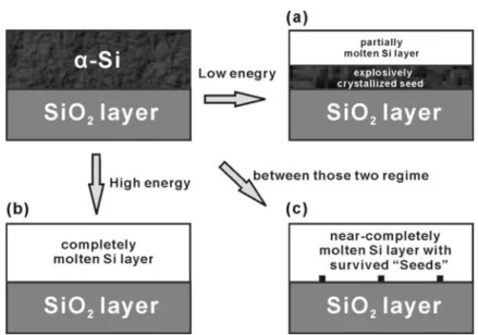
glass substrate. Moreover, as shown in Fig. 1-2, there are two major transformation
regimes (occurring at low and high laser energy, respectively) and one minor
transformation regime in between (that so-called superlateral growth, or SLG) [10], [11].
The low laser energy regime describes a situation where the incident laser is sufficient to
induce melting of the silicon films, but it is low enough that a continuous layer of silicon at
the maximum extent of melting. For this reason, this regime is referred to as the partial
melting regime. The high laser energy regime corresponds to a situation that the laser
energy is sufficiently high to completely melt the silicon film; this regime is also referred
to as complete melting regime. In addition to these two regimes, a third regime has been
found to exist within a very narrow experimental window in between the two main regimes.
Despite the small extent of this region, it is nonetheless one with great technological
significance, because the poly-Si films within the regime feature large-grained
polycrystalline microstructures [12]. The stable grain size of ELA poly-Si films is typically
limited to 0.3~0.6 μm. Larger grain size is possible within the SLG window, but this
Fig. 1-2 Illustration of transformation scenarios during the ELA process. Correspond to (a) partial melting, (b) completely melting and (c) near-completely melting of the initial Si film.
The surface roughness in ELA poly-Si films is localized at the planes and point of
congruence of grain boundaries. The mechanism for the formation of roughness is well
understood and is attributed to the specific density difference between molten Si (2.53 g
cm-3) and solid Si (2.30 g cm-3). In other words, as the molten Si solidifies, it
simultaneously expands. Solidification starts from neighboring seed areas, and the last
region to solidify is the volume at the vicinity of the two colliding lateral fronts. As that
Fig. 1-3 Solidification of the molten Si film. Resulting in the higher surface roughness
Although the highest quality poly-Si films were fabricated by ELA method, the poor grain size uniformity and high roughness ELA poly-Si films degraded the performance of TFT [13].
1.2.3. Continuous-wave laser crystallization (CLC) method
Hara et al. in 2001 announced highly crystalline poly-Si films on large-area glass
substrates by continuous-wave (CW) laser crystallization (CLC) [14]. In CLC, power
instability of diode pumped solid state (DPSS) CW laser (532nm (second harmonics (2ω)
of Nd:YVO4)) is less than 1%, which value is superior to that of XeCl excimer lasers and
Ar lasers. Moreover, CLC processes were conduced at room temperature and in ambient
environment. TFTs on such CLC poly-Si layers on glass substrates were fabricated at
process temperature below 450℃; field-effect mobilities for n-channels and p-channels
grains and low roughness in crystallized layers, in a quite wide energy range as shown in
Figure 1-3, because of continuous laser-energy supply, directional solidification caused by
laser scanning, and slow cooling rate of molten Si due to the dwell time of laser beam is
about 100 μs during scanning.
In 2007, Ogawa et al. [15] introduced CLC technologies to perform a low power (~
50mW) and high resolution (332ppi) VGA LCD with integrated 6-bit digital data drivers.
Excellent uniformity in threshold voltage, as compared to that of conventional ELA-TFTs,
is shown in Fig. 1-4 and Fig. 1-5.
Fig. 1-4 Global variation in NMOS threshold voltage: ELA (left), CLC (right). (L/W = 5.4μm/20μm, Tox = 30nm, TFT distance = 0.5mm) [15].
Fig. 1-5 Global variation in PMOS threshold voltage: ELA (left), CLC (right). (L/W = 2.7μm/20μm, Tox = 30nm, TFT distance = 0.5mm) [15].
1.2.4.
Ni metal-induced crystallization (MIC) / Ni metal-induced
lateral crystallization (MILC) methods
Solid phase crystallization of α-Si needed a high temperature and longer annealing time
for furnace annealing process. In the NIC/NILC method, the annealing time and
temperature could be reduced, and the grain size of NILC poly-Si films uniformly over
large area could be obtained [16]-[19]. In 2000, Sharp Corp. and SEL (Semiconductor
Energy Lab.) propose the CGSi (Continuous Grain Silicon) technique to fabricate the 60
inch HDTV rear projector [20]. When thin Ni is deposited on α-Si and annealed, Ni
disilicide (NiSi2) forms [21]. The nickel disilicide is cubic with CaF2 structure and has a
very close lattice parameter match to c-Si (-0.4%), the lattice constant of NiSi2, 5.406A, is
nearly equal to that of Si, 5.430A. The disilicide is actually the species that mediates the
transformation of α-Si to c-Si. As shown in Fig. 1-6, the c-Si formed below the Ni-pad is
Fig. 1-6 Schematic illustration of the Ni-metal induced Crystallization (MIC) and Ni-metal induced lateral crystallization (MILC)
The silicide mediate growth of silicon occurs in three stages. In the first stage,
precipitation and growth of NiSi2 occur in the temperature range of 325~400°C. In the
second phase, crystalline Si nucleates on one or more the eight {111} faces of the
octahedral NiSi2, as shown in Fig. 1-7. Finally, in the third phase, c-Si growth proceeds
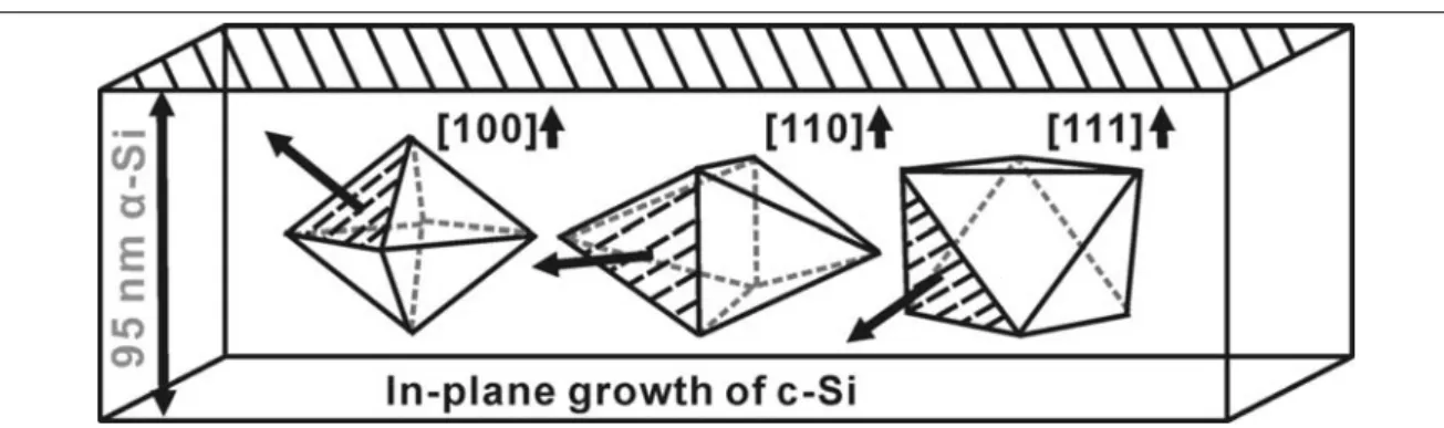
with a NiSi2 precipitate at the planar advancing growth front.
As shown in Fig. 1-7, for <110>-oriented precipitates, four of the {111} planes exhibit
surface normal within the planes of the film, which makes extensive growth possible. On
the other hand, the <100>- and <111>-oriented precipitates exhibits {111} planes normal
Fig. 1-7 Schematic representation of favorable precipitate orientations for long-range growth of epitaxial Si within the plane of the α-Si.
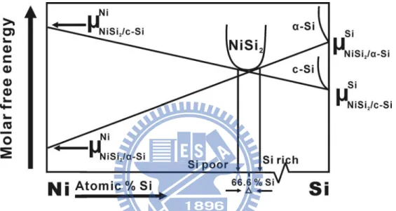
The driving force for the migration of NiSi2 precipitates is reduction in the free energy
associated with the transformation of meta-stable α-Si to stable c-Si. An equilibrium
free-energy diagram is provided for explanation, as shown in Fig. 1-8 [21]. It is well
known that the α-Si has a higher free energy than c-Si. In the case of Ni silicide mediated
crystallization, the free energy difference between Ni and Si atoms at the NiSi2/α-Si and
NiSi2/c-Si interface acts as the driving force for Ni diffusion [21]. The free energy of the
Ni atom is lower at the NiSi2/α-Si interface than at the NiSi2/c-Si interface, whereas the
free energy of the Si atom is lower at the NiSi2/c-Si interface. Therefore, with the
dissociative model [21], the NiSi2 layer dissociates to provide free Si for epitaxial growth
of c-Si at the c-Si/NiSi2 interface by the diffusion of Ni atoms. The Ni atoms diffuse to
α-Si following by formation of a fresh NiSi2/α-Si interface. Repetition of this process
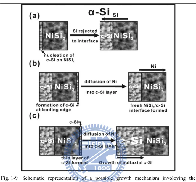
results in migration of NiSi2 precipitates through α-Si and growth of needlelike Si. Fig.
the formation of intermediate thin layer of c-Si on the leading edge of migrating NiSi2
precipitate [21]. As a result of this growth mechanism, NILC poly-Si films demonstrate a
needlelike microstructure, with each needle grain attribute to c-Si growth from an
individual disilicide precipitate.
Fig. 1-8 Schematic equilibrium molar free-energy diagram for NiSi2 in contact with α-Si
In addition to Ni, other metals have been investigated as far as their effectiveness in
enhancing Si crystal growth. These include Au [22], Al [23] and Sb [24] which form
Fig. 1-9 Schematic representation of a possible growth mechanism involoving the formation of a thin layer of c-Si at the NiSi2/α-Si interface
As a result, Ni remains the undisputed metal of choice for silicide-assisted
crystallization. It should be noted that traces of NiSi2 also remain within the c-Si that is left
behind after the growth phase. This would have presented an insurmountable obstacle had
it not been for the existence of an efficient gettering process [27], [28]. This process
utilizes the implantation of phosphorous, followed by low-temperature annealing to
effectiveness of the gettering process in removing the remaining silicide in the film after Si
crystallization [20], [29]. In practice, the necessity to maintain a low processing
temperature poses certain limitations on the quality of the poly-Si microstructure. One way
to boost the poly-Si quality is by combining MILC with laser annealing process to produce
high quality and good uniformity poly-Si films to realize the system-on-panel technology
[30]-[33].
In this thesis, we will focus on the Ni Metal induced lateral crystallization method. To
produce high performance LTPS TFTs by combined MILC and CLC method. Moreover,
discuss the growth mechanism of MILC and utilized fluorine ion implantation and CF4
plasma etching treatment to fabricate the LTPS TFT. And develop a simple method to
reduce the nickel impurity and passivate the trap-state density within the MILC
polycrystalline silicon films by drive-in method.
1.3.
Electrical properties of Ni metal-induced lateral
crystallization (MILC) thin-film transistors (TFTs)
stability due to large defect (trap state) density in MIC/MILC interface and MILC/MILC
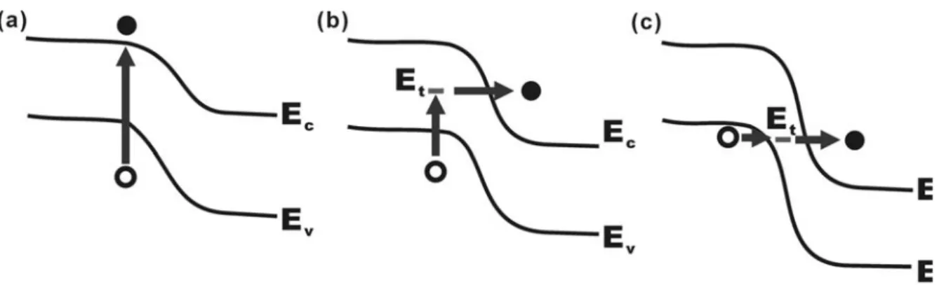
grain boundary and high Ni metal contamination [34]-[38]. Fig. 1-10 illustrates the leakage
current model using band diagrams [39]-[41], the first situation in Fig. 1-10 (a) is described
only the thermal activation of an electron from the valence band to the conduction band.
The second situation in Fig. 1-10 (b), the leakage current is induced by the trap or surface
state in the band gap. With increase the drain bias, the activation energy of leakage current
decreases, which suggests that the high field in the drain depletion region has reduced the
barrier that the electron must overcome. This situation comprises two steps: the first step is
the thermal activation of an electron from the valence band to a trap state (Et) in the band
gap, and the second step is electron tunneling through this reduced barrier to the
conduction band. As such, the dominant leakage current mechanism is thermionic field
emission. The third situation in Fig. 1-10 (c) is induced under strong electric field, in which
the dominant leakage current mechanism is pure tunneling. With the increase of the
electric field, the tunneling length decreases. The presence of the trap state in the band gap
assists the process by shorting the effective tunneling length of the electron. In addition,
the trap state in the band gap plays an important role in the leakage current model. In the
traditional MOSFET, those situations do not occur easily because the trap state is low. This
Fig. 1-10 The band diagram for the leakage current model. (a) Case of weak electric field. (b) Case of medium electric field. (c) Case of strong electric field.
Moreover, the Ni contamination of the MILC poly-Si films can degrade the minority
carrier life time and increase the leakage current. The leakage current is proportional to the
impurity concentration [42]-[43]. In order to solve the above problems, the post-annealing
treatment was proposed to reduce the MILC/MILC grain boundary defect density [44]-[46].
In the following, we will discuss the effects of grain boundary and Ni-metal impurity on
the electrical performance of MILC TFTs.
1.4. Reliability issue of poly-Si TFTs
boundary defects, and broken Si-H bonding so that stressed devices on poly-Si layers
normally show significant degradation in electrical characteristics [47]-[50]. In addition,
appropriate circuit and device design, the injection of energetic carriers into the gate
insulator and subsequent parameter shift through carrier trapping and trap state generation
poses one of the most significant long-term reliability concerns in the poly-Si TFTs. It
has been known that the application of high drain voltage and a relatively high gate voltage
(hot-carrier stressing) in poly-Si TFTs, decreases the maximum transconductance and
causes the shift of turn-on voltage. Therefore, a systematical study of the poly-Si TFTs
aging with stress time is required.
1.5. Motivation and organization of this thesis
In this thesis, the major research subject is Ni metal induced lateral crystallization of
amorphous silicon, which involved of the trap-state density, reliability and uniformity
effects on the MILC poly-Si TFTs electrical properties. It has been reported that
continuous-wave (CW) laser crystallization (CLC) of α-Si has also been recently employed
to fabricate high-performance LTPS TFTs. Compared with excimer laser crystallization
(ELC) process; the CLC process was simpler, easier and relatively inexpensive.
Unfortunately, their uniformity was poor because the shape of beam profiles was Gaussian.
to crystallize at a temperature below 600°C. Three stages have been identified in the MILC
crystallization process: (1) the formation of NiSi2 precipitates, (2) the nucleation of
crystalline silicon (c-Si) on {111} faces of octahedral NiSi2 precipitates and (3) the
subsequent migration of NiSi2 precipitates and crystallization of needlelike Si grain.
Unfortunately, the needlelike grain boundaries easily trap Ni and NiSi2 precipitates
which increase the leakage currentand shift the threshold voltage. In order to eliminate the
trap states of poly-Si film a hydrogen plasma treatment process has been utilized to
improve the device performance. However, the hydrogen concentration in the poly-Si film
was hard to control, and the formed Si-H bonds were too weak to resist the hot carrier
generation. Therefore, the TFT devices of MILC poly-Si in order to provide high
performance, the improvement of the uniformity, trap-state density, Ni contamination and
reliability were need to be investigated.
This thesis is organized into five parts:
In Chapter 2, to improve the uniformity of CLC-TFT and MILC-TFT, a new method for
uncomplicated and effective method to originate fluorine atoms into MILC poly-Si films.
In Chapter 4, CF4 plasma was employed to improve the electrical performance of
conventional MILC TFTs. This uncomplicated and effective method involves etching
away the top surface of MILC poly-Si and passivating the trap states.
In Chapter 5, a novel fabrication process has been developed to reduce the Ni
concentration and minimizes the trap-state density of MILC TFTs using nickel drive-in
induced laterally crystallization (DILC). The DILC poly-Si was prepared by collision
between fluorine ion (F+) implantation and Ni through the designed pattern into α-Si layer.
Chapter 2
Electrical characteristics and stability of
poly-Si TFTs fabricated by continuous-wave
laser annealing of metal-induced lateral
crystallized silicon films
2.1. Introduction
Low-temperature polycrystalline silicon (LTPS) thin-film transistors (TFTs) have
attracted considerable interest for their application in organic emitting diode displays and
liquid crystal displays, since they exhibit good electrical properties and can be integrated in
peripheral circuits on inexpensive glass substrates [51].For the application to system on
Ni-metal-induced lateral crystallization (MILC) is one of these efforts. In MILC, Ni islands
are selectively deposited on top of α-Si films and allowed to crystallize at a temperature
below 600°C [32], [52].Continuous-wave (CW) laser crystallization (CLC) of α-Si has
also been recently employed to fabricate high-performance LTPS TFTs[53]-[56].
Compared with excimer laser crystallization (ELA) process, the CLC process was simpler,
easier and relatively inexpensive. Unfortunately, their uniformity was poor because the
shape of beam profiles was Gaussian [57].
To improve the uniformity of CLC-TFT, a new method for fabricating MILCLC-TFT
was proposed in this letter. Instead of α-Si, MILC-Si film was irradiated by CW laser of
various output powers.
2.2. Experiment procedure
Two kinds of Si films (α-Si and MILC-Si) were irradiated by CW laser at room
temperature in an air atmosphere. Samples designated as “CLC” were α-Si films and those
designated as “MILCLC” were MILC-Si films irradiated by CW laser.
2.2.1. CLC poly-Si TFTs
A four-inch quartz wafer with a 500-nm-thick wet oxide layer was used as the substrate.
using low-pressure chemical vapor deposition (LPCVD). To form the CLC-Si film, α-Si
films were then irradiated using a CW laser of various output powers (2.5 W, 3.8 W and 5
W). Reactive ion etching (RIE) was employed to form islands of poly-Si regions on the
wafers. Next, a 100-nm-thick tetraethylorthosilicate/O2 oxide layer was deposited as the
gate insulator by plasma-enhanced chemical vapor deposition (PECVD). Then a
200-nm-thick poly-Si film was deposited as the gate electrode by LPCVD. After defining
the gate, self-aligned 40 keV phosphorous ions were implanted at a dose of 5 × 1015 cm-2 to
form the source/drain and gate. Dopant activation was performed at 600°C in N2 ambient
for 24 h. Contact holes were formed and a 500-nm-thick Al layer was then deposited by
thermal evaporation and patterned as the electrode. Sintering process was performed at
400°C for 30 min.
2.2.2. MILCLC poly-Si TFTs
A four-inch quartz wafer with a 500-nm-thick wet oxide layer was used as the substrate.
To form the α-Si film, a silane-based undoped α-Si layer of 100 nm thick was deposited
laser was parallel to the MILC needlelike poly-Si grains.Reactive ion etching (RIE) was
employed to form islands of poly-Si regions on the wafers. Next, a 100-nm-thick
tetraethylorthosilicate/O2 oxide layer was deposited as the gate insulator by
plasma-enhanced chemical vapor deposition (PECVD). Then a 200-nm-thick poly-Si film
was deposited as the gate electrode by LPCVD. After defining the gate, self-aligned 40
keV phosphorous ions were implanted at a dose of 5 × 1015 cm-2 to form the source/drain
and gate. Dopant activation was performed at 600°C in N2 ambient for 24 h. Contact holes
were formed and a 500-nm-thick Al layer was then deposited by thermal evaporation and
patterned as the electrode. Sintering process was performed at 400°C for 30 min.
2.3. Results and discussion
2.3.1. SEM analysis of CLC poly-Si films
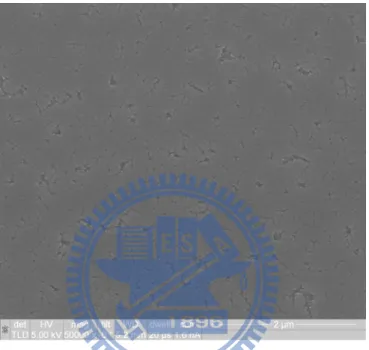
Fig. 2-1 to Fig. 2-3 shows SEM images of the Secco-etched CLC irradiated under
various laser output powers. As can be seen, the CLC poly-Si comprises grains of various
sizes distributed in three distinct regions [57]. As shown in Fig. 2-1, at laser output power
of 2.5 W, CLC-2.5 was found in the solid phase crystallization (SPC) region with fine
grains. With increasing laser output power, CLC-3.8 was in the partially melted region
power reached 5.0 W, CLC-5.0 was in the completely melted region. As seen in Fig. 2-3,
the uniformity of CLC-5.0 grains was poor. It contained both ELC poly-Si-like grains and
very large directional grains.
Fig. 2-1 SEM images of Secco-etched poly-Si grains irradiated by CW laser with CLC-2.5 W
Fig. 2-2 SEM images of Secco-etched poly-Si grains irradiated by CW laser with CLC-3.8 W
Fig. 2-3 SEM images of Secco-etched poly-Si grains irradiated by CW laser with CLC-5.0 W
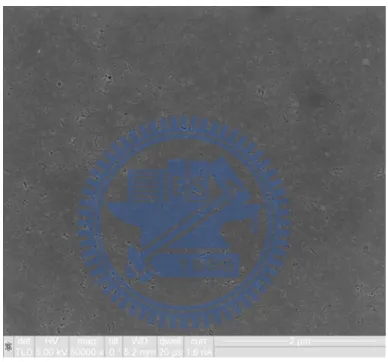
2.3.2. SEM analysis of MILCLC poly-Si films
Fig. 2-4 to Fig. 2-6 shows SEM images of the Secco-etched MILCLC irradiated under
various laser output powers. As for the fabrication of the MILCLC poly-Si, Fig. 2-4 shows
that at lower laser output power, the sizes and shapes of MILCLC-2.5 needle Si grains
were similar to those of MILC poly-Si. This is because MILCLC-2.5 was in the SPC
region. Only some of the α-Si regions among Si grains were melted and crystallized. When
the laser output power reached 3.8 W, the width of MILCLC-3.8 grains increased to 3 μm,
as shown in Fig. 2-5. Compared with that of CLC-3.8, the grain size of MILCLC-3.8 was
larger and the uniformity was better. We believe that most of the a-Si and small MILC
grains in this regime were molten. However, the large grains were only molten partially
and served as predetermined nuclei for grain growth. The width of these grains increased
markedly due to the geometrical coalescence of Si needle grains. Geometrical coalescence
can be simply described as an encounter of grains whose relative orientations are similar
The crystal structure of MILCLC-5.0 was similar to that of CLC-5.0. It contained both
ELC poly-Si-like grains and very large directional grains. As shown in Fig. 2-6, the
uniformity of MILCLC-5.0 grains was poor. This is because MILCLC-5.0 was in the
completely melted region.
Fig. 2-4 SEM images of Secco-etched poly-Si grains irradiated by CW laser with MILCLC-2.5 W
Fig. 2-5 SEM images of Secco-etched poly-Si grains irradiated by CW laser with MILCLC-3.8 W
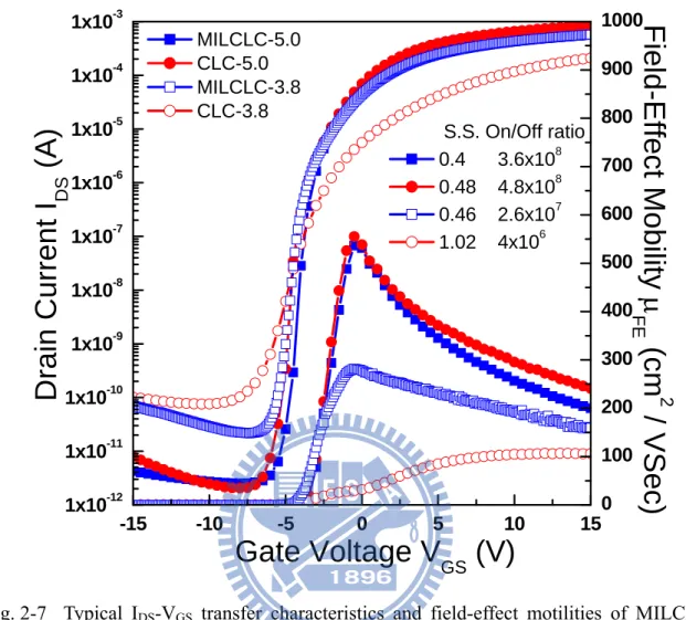
2.3.3. Electrical properties of CLC and MILCLC TFTs
Fig. 2-7 shows the transfer characteristics and field-effect mobility versus the gate
voltage of TFTs in the random grain structure for W = L = 20 μm at VDS = 5 V and VDS =
0.1 V, respectively. The measured and extracted key device parameters are also
summarized in Fig. 2-7. The threshold voltage (Vth) was defined as the gate voltage
required to achieve a normalized drain current of IDS = (W / L) × 100 nA at VDS = 5 V. It
was found that when the laser output power was 5.0 W, the electrical performance of
MILCLC-5.0 and CLC-5.0 were similar, both showing excellent performance. This is
because they were in the completely melted region. Both Si films had very large
-15 -10 -5 0 5 10 15 1x10-12 1x10-11 1x10⁻¹⁰ 1x10⁻⁹ 1x10⁻⁸ 1x10⁻⁷ 1x10⁻⁶ 1x10⁻⁵ 1x10⁻⁴ 1x10⁻³
Drain Current I
DS(A
)
Gate Voltage V
GS(V)
MILCLC-5.0 CLC-5.0 MILCLC-3.8 CLC-3.8 0 100 200 300 400 500 600 700 800 900 1000 S.S. On/Off ratio 0.4 3.6x10⁸ 0.48 4.8x10⁸ 0.46 2.6x10⁷ 1.02 4x10⁶Field-Effect Mobility
μ
FE(cm
2/ VSec)
Fig. 2-7 Typical IDS-VGS transfer characteristics and field-effect motilities of MILCLC and CLC TFTs (W/L=20 μm/20 μm)
However, the performance of MILCLC-3.8 and CLC-3.8 TFTs were quite different
when the laser output power was 3.8 W. Compared with CLC-3.8 TFTs, MILCLC-3.8
most of these coalescence grains and their boundaries were parallel to the drain current
(Ids), which reduced the impedance to carrier flow. This in turn decreased the threshold
voltage and increased greatly the mobility and Ion/Ioff current ratio.
The electrical characteristics of both CLC-2.5 and MILCLC-2.5 were not as good as
those of other TFTs. The performance of CLC-2.5 TFT was similar to that of SPCsince
CLC-2.5 film contained SPC poly-Si-like grains. On the other hand, the performance of
MILCLC-2.5 TFT was similar to that of MILC-Si since only some of the α-Si regions
among MILC grains were melted. As a result, the mobility of CLC-2.5 was 4.1 cm2/Vs,
while that of MILCLC-2.5 was 50 cm2/Vs [60].
2.3.4. Uniformity of CLC and MILCLC TFTs
The other important issue of poly-Si TFTs is their uniformity for the application on SOP
and solar cells. As shown in Fig. 2-8, 10 TFTs were measured in each case to investigate
the device-to-device variation. TABLE 2-1 lists the average values of the field-effect
mobility and threshold voltage of TFTs with standard deviations in parentheses. Since the
electrical characteristics of CLC-2.5 and MILCLC-2.5 were poor, their uniformities were
not listed here. Although the mobility of both MILCLC-5.0 and CLC-5.0 was high, their
uniformity was poor and their standard deviations were large. This is because both films
grains. The uniformity of CLC-3.8 and MILCLC-3.8 was much better and their standard
deviations were small. As mentioned previously, MILCLC-3.8 has uniformly distributed
geometrical coalescence grains. As a result, MILCLC-3.8 has the smallest standard
deviation. 100 200 300 400 500 800 900 1000 0 20 40 60 80 100 MILCLC-5.0 CLC-5.0 MILCLC-3.8 CLC-3.8
Field-Effect Mobility
μ(cm
2/ Vs)
Cu
mu
lative
Percen
tag
e (%)
-9 -8 -5 -4 0 20 40 60 80 100Threshold Voltage V
TH(V)
Cum
u
lat
ive Percentage (%)
TABLE 2-1 Average values of field-effect mobility and threshold voltage of two different structures with standard deviations in parentheses.
TFT (W = L = 20 μm) Field-effect Mobility (cm2/Vs)μFE Threshold Voltage (V) VTH MILCLC-5.0 421 (62) -4 (0.34) CLC-5.0 394 (152) -3.9 (0.31) MILCLC-3.8 288 (7.2) -4.19 (0.13) CLC-3.8 112 (13) -4.08 (0.21)
2.4. Conclusion
To improved uniformity and electrical performance of CLC-TFTs, two kinds of Si films
(α-Si and MILC-Si) were used in this study. After irradiated by CW laser of various output
powers (2.5 W, 3.8 W and 5 W), it was found that the performance and uniformity of
MILCLC-TFTs were better than those of CLC-TFTs. When the laser output power was
low (2.5 W), both films were in the SPC region. Only some of the α-Si regions were
melted. The electrical characteristics of CLC-2.5 and MILCLC-2.5 were poor. When the
laser output power reached 5.0W, CLC-5.0 and MILCLC-5.0 were in the completely
melted region. They both showed excellent performance. Unfortunately, the uniformity
was poor because they contained two kinds of grains: ELC poly-Si-like grains and very
large directional grains. When the laser output power was median (3.8 W), CLC-3.8 and
performance and uniformity of MILCLC-3.8 were much better than those of CLC-3.8.
This is because the width of the MILCLC-3.8 grains increased dramatically due to the
geometrical coalescence of MILC-Si needle grains. Moreover, the uniformity of
MILCLC-3.8 was far superior to that of CLC-5.0 and MILCLC-5.0, and therefore was
Chapter 3
Effect of the F
+implantation on the electrical
characteristics and reliability of MILC poly-Si
TFTs
3.1. Introduction
In recent years low-temperature polycrystalline silicon (LTPS) thin-film transistors
(TFTs) have attracted considerable interest for their use in active-matrix liquid crystal
displays (AMLCDs) since they exhibit good electrical properties and can be integrated in
peripheral circuits on inexpensive glass substrates [51]. Since poly-Si thin film transistors
(TFTs) require glass substrates, intensive studies have been carried out reducing the
crystallization temperature of amorphous silicon (α-Si) films. Ni-metal-induced lateral
crystallization (MILC) is one of these efforts. In MILC, Ni islands are selectively
deposited on top of α-Si films and allowed to crystallize at a temperature below 600°C [32],
[52]. Three stages have been identified in the MILC crystallization process: (1) the
faces of octahedral NiSi2 precipitates and (3) the subsequent migration of NiSi2 precipitates
and crystallization of needlelike Si grain [21].
Unfortunately, the needlelike grain boundaries easily trap Ni and NiSi2 precipitates
which increase the leakage currentand shift the threshold voltage [34], [36], [37], [61],
[62]. In order to eliminate the trap states of poly-Si film a hydrogen plasma treatment
process has been utilized to improve the device performance [63].However, the hydrogen
concentration in the poly-Si film was hard to control, and the formed Si-H bonds were too
weak to resist the hot carrier generation.
In this section, a sample manufacture method using fluorine-ion implantation was
proposed for MILC poly-Si TFTs. The advantage of this technique is to provide an
uncomplicated and effective method to originate fluorine atoms into MILC poly-Si films.
The electrical characteristics including I-V measurement, trap-state density, activation
energy (EA), on/off ratio, and hot carrier stress on threshold voltage shift (ΔVTH) are
reported in this work.
(LPCVD) system. The photoresist was patterned to form the desired Ni lines, and a
20-Å-thick Ni film was deposited on the α-Si. The samples were then dipped into an
acetone for 5 min to remove the photoresist, and subsequently annealed at 540°C for 18 h
to form the MILC poly-Si film. To reduce Ni contamination, the unreacted Ni metal was
removed by chemical etching. Reactive ion etching (RIE) was employed to form islands of
poly-Si regions on the wafers. Fluorine ions were then implanted into the MILC film. The
projection range of fluorine-ions was set at the middle of MILC layer thickness. The
dosage of fluorine ions and ion accelerating energy were 2×1013 cm-2 and 30 KeV,
respectively. Next, a 100 nm thick SiH4/N2O oxide layer was deposited as the gate
insulator by plasma-enhanced chemical vapor deposition (PECVD). Then, a 200 nm thick
poly-Si film was deposited as gate electrode by LPCVD. After defining the gate,
self-aligned 40 KeV phosphorous ions were implanted at a dose of 5×1015 cm-2 to form
source/drain and gate. The F+-implanted MILC film and the P+31-implanted
source/drain/gate were then annealed/activated at 600°C for 24 h. A 500 nm thick SiO2
film was deposited by PECVD to serve as a passivation layer. Contact holes were opened
through the oxide layer, and 500 nm of aluminum (Al) was deposited, defined, and etched
to form the metal pads. Finally, the finished MILC poly-Si TFT devices were sintered in a
MILC TFTs (2×1014 cm-2 and 2×1015 cm-2) were also investigated. 3.8 W
wet oxide
a-Si
MILC poly-Si Gate-oxide poly-gateSubstrate
a-Si
MILC poly-Si F-implant P-implant F-ion dose : 2 × 10¹³; 30 KeV P-ion dose : 5 × 10¹⁵; 40 KeV Thermal annealing 600oC 24 hr 3.8 Wwet oxide
a-Si
MILC poly-Si Gate-oxide poly-gateSubstrate
a-Si
MILC poly-Si F-implant P-implant F-ion dose : 2 × 10¹³; 30 KeV P-ion dose : 5 × 10¹⁵; 40 KeV Thermal annealing 600oC 24 hrFig. 3-1 Schematic diagrams of process flow of MILC poly-Si TFTs with and without F+ implantation.
3.3. Results and discussion
3.3.1.
Electrical properties of MILC-TFTs with and without F
+implantation
required to achieve a normalized drain current of IDS = (W / L) × 100 nA at VDS = 5 V. The
subthreshold slope (SS) and Vth of the F+-implanted MILC TFTs were 1.1 V/dec. and 5.9 V,
which were superior to 2.0 V/dec. and 9.2 V of MILC TFTs. The ON/OFF current ratios of
the MILC poly-Si TFTs with and without the F+ implant treatment were 9.91×10⁶ and
3.72×10⁶ at VDS = 5 V, respectively. The output characteristic is shown in Fig. 3-3,
exhibiting the better improvement at a drain current of the F+-implanted MILC TFTs at
VGS = 12 V and 20 V. These improvements were attributed to the reduction of the defects
in the poly-Si film. In MILC poly-Si, Ni-related defects may degrade electric performance
because they introduce trap states including dangling bonds and strain bonds. Most of these
defects were located at the MILC poly-Si/buffer-oxide interface since high Ni contents
-5 0 5 10 15 20 25 30 1x10-12 1x10-11 1x10⁻¹⁰ 1x10⁻⁹ 1x10⁻⁸ 1x10⁻⁷ 1x10⁻⁶ 1x10⁻⁵ 1x10⁻⁴ W / O F+ implantation F+ 2 x 1013 cm-2 W / L = 10 μm / 10 μm
Gate Voltage V
GS(V)
Dra
in Cu
rr
en
t I
DS(A)
0 20 40 60 80 100 120 140 160 180 200 VDS = 0.1 V V DS = 5 VFie
ld-Effect Mob
ility
μ
FE(cm
2/V
sec)
Fig. 3-2 The transfer characteristics and field-effect mobility of the MILC poly-Si TFTs with and without F+ implantation.
TABLE 3-1 Device characteristics of the MILC poly-Si TFTs with and without F+ implantation
Field-effect mobility (cm2 / V-s) Subthreshold slope (V / dec) Threshold voltage Vth (V) ON/OFF current ratio
9.2 3.72 × 10⁶ Device Parameters 95 5.9 9.91 × 10⁶ 1.1 Without F+-implantation F+-implantation 2×1013cm-2 49 2.0 F+-implantation 2×1014cm-2 70 7.9 5.69 × 10⁶ 1.5
0 5 10 15 0.0 2.0x10⁻⁵ 4.0x10⁻⁵ 6.0x10⁻⁵ 8.0x10⁻⁵ 1.0x10⁻⁴ 1.2x10⁻⁴ 1.4x10⁻⁴
V
GS= 12 V
V
GS= 20 V
Dr
a
in Cur
re
n
t I
DS(A
)
Drain Voltage V
DS(V)
W / O F
+implantation
F
+2 x 10
13cm
-2Fig. 3-3 Output characteristics of the MILC poly-Si TFTs with and without F+ implantation.
3.3.2. SIMS analysis of F
+implantation Poly-Si film
As shows in Fig. 3-4, secondary ion mass spectrometry (SIMS) depth profile analysis
characteristics. 0 20 40 60 80 100 120 140 160 180 200 102 103 104 105
B uffer-O xide
P oly-S i C hannel
Intensity (counts)
D e p th (n m )
F lu o rin e
N ick e l
Fig. 3-4 SIMS depth profile of fluorine and nickel in the structure of interface of MILC poly-Si/buffer oxide film after annealing at 600℃ for 24 hr
3.3.3. Influence of F
+implantation on trap-state density
The trap state densities (Nt) of TFTs were extracted using Levinson and Proano’s
method, which can estimate the Nt from the slope of the linear segment of ln [IDS /
(VGS-VFB)] vs. 1 / (VGS-VFB)2 at low VDS and high VGS, where VFB is defined as the gate
3-5, the conventional MILC poly-Si TFT exhibits a Nt of 6.29×1012 cm-2, whereas the F+
implantation 4.24×1012 cm-2. The reduction in Nt values implies that those defects have
been effectively terminated using F+ implantation.
0 2 4 -20 -19 -18 -17 -16 -15
N
t= 6 .2 9 x 1 0
12cm
-2N
t= 4 .2 4 x 1 0
12cm
-2ln [I
DS/ (V
GS-V
FB)] (
Ω
-1)
1 /(V
G S- V
F B)
2(1 0
-3V
-2)
W / O F
+im plantation
F
+2 x 10
13cm
-2Fig. 3-5 The trap state densities (Nt) of TFTs. They can be estimated from the slope of the linear segment of ln [IDS / (VGS-VFB)] vs. 1 / (VGS-VFB)2 at low VDS and high VGS.
temperature ranging from 25 to 125℃ [67]. It reflects the carrier transportability, which is
related to the barrier height in the poly-Si channel. The lower the EA, the lower the carrier
transport barrier will be. Fig. 3-6 shows the EA of drain current as a function of gate voltage
measured at VDS = 0.1 V. The EA of F+-implanted MILC TFTs was less than that of MILC
TFTs. In other words, during the thermal annealing process, fluorine ions lowered the
barriers (passivated the trap states) in the MILC poly-Si film, and led to improve the
electrical characteristics. However, as shown in TABLE 3-1, the reduction in the Nt did not
suppress the minimum off current of the F+-implanted device. Similar results have been
reported in other poly-Si TFTs which were passivated by the F+ implantation and CF4
plasma treatment [68]-[70].The F+ implantation did not improve the minimum off current
0 10 20 30 0.0 0.1 0.2 0.3 0.4 0.5 0.6 0.7
Actication Energy E
A(eV
)
Gate Voltage V
GS(V)
W / O F
+implantation
F
+2 x 10
13cm
-2Fig. 3-6 The activation energy (EA) of drain current as a function of gate voltage measured at VDS = 0.1 V.
Electrical properties of the F+-implanted MILC poly-Si TFTs with different dosages
an optimal F+ implantation dosage of 2×1013 cm-2. However, the electrical characteristics
of F+-implanted TFTs are degraded as the implantation dosage increases. This is because
when the dosages were higher than Si solid solubility, the trap-state density and fluorine
clusters increased with the dosage [71]. When dosage reached 2×1015 cm-2, the device
performance was very poor.
-5 0 5 10 15 20 25 30 1x10-12 1x10-11 1x10⁻¹⁰ 1x10⁻⁹ 1x10⁻⁸ 1x10⁻⁷ 1x10⁻⁶
W / L = 10
μ
m / 10
μ
m
V
DS= 0.1 V
Dr
ai
n Cur
re
nt
I
DS(A
)
Gate Voltage V
GS(V)
W /O F
+implantation
F
+2 x 10
13cm
-2F
+2 x 10
14cm
-2Fig. 3-7 Typical IDS-VGS transfer characteristics of MILC poly-Si TFTs and F+-implanted MILC poly-Si TFTs with various dosages.
3.3.4. Reliability of MILC poly-Si with and without F
implantation
The other important issue of poly-Si TFTs is their reliability, which was examined underhot-carrier stress. Fig. 3-8 is a plot of the ΔVTH versus stressing time at VGS = 15 V and
VDS =25 V. The threshold voltages of TFTs were degraded because dangling bonds were
created at weak Si-Si bonds and Si-H bonds, which trapped electrons [72], [73].
Fortunately, this threshold voltage degradation was improved by F+ implantation.
F+-implanted TFTs possessed high immunity against the hot-carrier stress and thereby
exhibit lower ΔVTH than that of typical MILC TFTs. This is because weaker Si-H and Si-Si
bonds were replaced by stronger Si-F bonds. As a result, the electrical reliability of
0 1000 2000 3000 4000 5000 0 5 10 15 20 25 30 35 40
W /O F
+im plantation
F
+2 x 10
13cm
-2F
+2 x 10
14cm
-2Threshold Voltage S
h
ift
Δ
V
TH(%)
Stress Tim es (s)
Stressed at V
G S= 15 V, V
D S= 25 V
M easured at V
DS= 5 V
Fig. 3-8 Threshold voltage variation versus stress time of the MILC poly-Si TFTs with and without F+ implantation.
3.4. Conclusion
In summary, the effect of the F+ implantation on the electrical characteristics and
reliability of MILC poly-Si TFTs was investigated. The fluorine ion accelerating energy
was 30 KeV. After annealing at 600°C for 24 h, it was found that F+-implanted TFT
higher ON/OFF current ratio, and lower trap state density (Nt) as compared with typical
MILC TFT. It was also found F+ implantation process can greatly improve the electrical
reliability under a hot-carrier stress. This is because weaker Si-H and Si-Si bonds were
replaced by stronger Si-F bonds. As a result, F+-implanted TFTs possessed high immunity
against the hot-carrier stress and thereby exhibit lower ΔVTH than that of typical MILC
Chapter 4
Influence of etching treatment on electrical
and reliability of MILC poly-Si TFTs using CF
4Plasma
4.1. Introduction
In recent years low-temperature polycrystalline silicon (LTPS) thin-film transistors
(TFTs) have attracted considerable interest for their use in active-matrix liquid crystal
displays (AMLCDs) since they exhibit good electrical properties and can be integrated in
peripheral circuits on inexpensive glass substrates [51]. Since poly-Si thin film transistors
(TFTs) require glass substrates, intensive studies have been carried out reducing the
crystallization temperature of amorphous silicon (α-Si) films. Ni-metal-induced lateral
crystallization (MILC) is one of these efforts. In MILC, Ni islands are selectively
deposited on top of α-Si films and allowed to crystallize at a temperature below 600°C [32],
[52]. Three stages have been identified in the MILC crystallization process: (1) the
![Fig. 1-1 Roadmap of poly-Si TFT technology. [6]](https://thumb-ap.123doks.com/thumbv2/9libinfo/8748568.205407/22.892.185.725.439.767/fig-roadmap-of-poly-si-tft-technology.webp)