國 立 交 通 大 學
電信工程學系
碩 士 論 文
6GHz 縮小化頻率調變連續波雷達系統
6GHz Compact Size
Frequency Modulation Continuous Wave
Radar System
研究生 :
陳 諭 正 (Yu-Cheng Chen)
6GHz 縮小化頻率調變連續波雷達系統
研究生:陳諭正 指導教授:鍾世忠 教授 國立交通大學電信工程學系摘要
本篇論文是一套 6GHz 縮小化 FMCW 雷達。從天線到射頻模組以及 FMCW 演算 法的改進。天線部份其一是超寬頻天線架構。有別於傳統超寬頻天線大多是用一 大片金屬來當輻射體或是多個不同頻段之天線來達到寬頻的要求,此天線架構是 利用一段靠近地的間隙來使天線的輸入阻抗在極大的頻寬內沒有很大的變化。此 天線架構類似常見的倒 F 型天線(Inverted-F antenna),但縮小天線與地的間 距,即可得到一相當寬頻的天線。另一個是天線陣列,使用槽孔天線當天線元件 做成的 2x1 的天線陣列。來滿足所需之天線指向性。 FMCW 雷達演算法改進是基於學長之前所做的 24GHz FMCW 雷達系統再加以改 良。本來是用一連串的鋸齒波,並對回波訊號做 2D 的 FFT 來達到偵測目標物距 離與相對速度的功能。但舊有的演算法須要較大的運算量以及較高的硬體要求, 所以我用了不同的調變方法。有別於一連串的鋸齒波調變,我使用一個較慢的三 角調變波,可避免相度速度的影響,且大幅減少運算量以及硬體的要求。此外, 為了在有限頻寬內提高距離解析度,所以加入了補零的動作,並根據舊有的訊號 特性改進了原來的中頻放大器。在距離解析度上至少提高了一倍的準確度,改進 後的中頻放大器也讓雷達系統的靈敏度提高 10dB 以上。 6GHz FMCW 縮小化射頻模組,跟 24GHz FMCW 雷達不一樣。為了縮小化所以 使用同一根天線當接收與發射使用。且系統中只使用了一個 6GHz 壓控震盪器以 及一個平衡混頻器。使用單天線會受到天線特性而對系統靈敏度有很大的影響,6GHz FMCW Radar System
Student:Yu-Cheng Chen Advisor:Dr.Shyh-Jong Chung Electrical and Computation Engineering
National Chiao Tung University
Abstract
A 6GHz compact size radar system is proposed in this article. There are several parts; antenna, Rf module and DSP improvement. This article proposed two different kinds of antenna. One is a novel wideband antenna. A small gap between radiator and ground smoothes the input impedance variation. The antenna structure proposed quite like a Inverted-F antenna. Just lower the gap size, this common antenna type comes a wideband antenna. Another proposed antenna is a 2x1 aperture couple antenna array. Aperture couple antenna has good directivity naturally. So a array with two antenna element can satisfied the requirement.
Digital signal processing is base on the previous approach and adds some improvement. 2D FFT is used in previous approach. Using different control wave can save system resource and 1D Chirp Transform is enough. Zero padding technology is also used to improve distance and relative velocity resolution. And a modified IF amplifier is also proposed. This amplifier upgrades system sensitivity to 10dB better.
only. Not like 24GHz radar system, this radar system uses the same antenna for Tx/Rx. Using single antenna can save half antenna area but the characteristic of antenna affects a lot. Base on the experience in 24GHz radar system there are some approaches to suppress the effect of antenna and implement this compact size radar system successfully.
誌謝
從交大電信系一直到交大電信所,專題加碩士班修業的三年多時間,在微波 這方面獲得相當多的知識。當然要先感謝鍾世忠教授這三年多的教導。從教授身 上學到了很多天線的知識,更學到了許多處世的道理。實驗室在教授的帶領下也 是在歡樂氛圍裡運轉著。謝謝實驗室的成員:高壓老何,好人飄,壞人嘴炮信, 打屁宗,鑣哥,凱凱,助益非淺Q仔,峰哥,克老二,流氓彥圻,陳壞人,敦智, 大將彥志,達叔,小花,小巴,小建宏,小黃,沒0,楊碰碰,煥昇,鳥U,阿雷, 蘇警棍,馬爺,阿本。你們的垃圾話,讓實驗室在研究之餘笑聲連連。尤其是雷 達三小跟烙跑學弟煥昇,非常謝謝,有你們。 不只實驗室裡成員,還有許許多多系上教授以及同學學弟妹,都讓人在回首 過去時,不經露出了笑容。謝謝張大大,壹哥,謝小福,你們教了我很多東西。 謝謝嘟嘟,阿胖,好人鳥U,北七小花,北七阿普,米尼米,康康,最認真的英 公,不老實的梁八,俊哥,維婷。有你們,真是一段無腦但相當珍貴的回憶。 最後感謝家人全力的支持,讓我在迷惘無力的時刻,又站了起來,堅持到底。Contents
1 Introduction of Radar system 1
1.1 Background . . . 1
1.2 Radar System Basic Principle and Radar System Introduction . . . 2
1.3 FMCW Radar Distance and Velocity Detection . . . 5
2 24GHz FMCW Radar System 7 2.1 24GHz FMCW Radar System Architecture . . . 7
2.2 24GHZ FMCW Radar System Algorithm . . . 8
2.2.1 Signal Processing Flow Chart . . . 8
2.2.2 Chirp Transform . . . 11
2.2.3 UART Protocol . . . 13
3 Improvement of Radar system 15 3.1 Previous Approach in Algorithm (2D-FFT) . . . 15
3.2 New Approach in Algorithm . . . 17
3.2.1 Triangular Control Wave . . . 17
3.2.2 Triangular Control Wave Test Result . . . 18
3.2.3 Zero Padding . . . 19
4 6GHz Compact Size FMCW Radar System 25
4.1 Novel Wideband Antenna Con…guration . . . 26
4.1.1 Antenna structure and Parameter discussion . . . 27
4.1.2 Antenna Pattern . . . 33
4.2 Aperture Couple Antenna Array . . . 36
4.2.1 Aperture Couple Antenna Array Con…guration . . . 36
4.2.2 Return Gain and Antenna Pattern . . . 37
4.3 Compact Size Low-pass Filter . . . 38
4.4 Hybrid Mixer . . . 39
4.4.1 Hybrid Mixer Improvement and Test Result . . . 41
4.5 Voltage Control Oscillator . . . 42
5 6GHz FMCW Radar System Integration and Measurement 44
List of Figures
1-1 Diagram of Radar System . . . 3
1-2 (a) Pulse Radar Diagram (b) FMCW Radar diagram . . . 4
1-3 Frequency Modulation Wave and Receiving Signal without Relative Velocity 4 1-4 Frequency Modulation Wave and Receiving Signal without Relative Velocity 5 2-1 24GHz FMCW Radar System Architecture . . . 8
2-2 FMCW Radar Digital Signal Flow Chart . . . 9
2-3 C Code of the Interrupt Subroutine . . . 9
2-4 Diagram of Chirp Transform . . . 11
2-5 C Code of Chirp Transform . . . 13
2-6 Protocol of UART . . . 14
3-1 First FFT Operation . . . 16
3-2 Second FFT Operation . . . 16
3-3 Triangular Control Wave . . . 18
3-4 Test Result of Rising Part . . . 19
3-5 Test Result of Falling Part . . . 19
3-6 (a) Diagram of Zero Padding (b)Diagram of Chirp Transform Calculation with Zero Padding . . . 20
3-7 (a)128 points 5.7KHz sine waveform (b) Test Signal with Blackman Win-dow and Zero Padding . . . 21
3-8 (a) Without Zero Padding Frequency Result (b)With Zero Padding
Fre-quency Result . . . 21
3-9 IF Signal in Previous IF Ampli…er . . . 22
3-10 FFT Result of IF Signal . . . 22
3-11 Diagram of the Limitation in Frequency Domain . . . 23
3-12 (a) Frequency Response of Previous IF Ampli…er (b) Frequency Response of New IF Ampli…er . . . 24
3-13 (a) Test Result with Previous IF Ampli…er (b) Test Result with New IF Ampli…er . . . 24
4-1 6GHz Compact Size FMCW Radar Block Diagram . . . 26
4-2 Con…guration of Inverted-F Antenna . . . 27
4-3 Geometry of Novel Wideband Antenna . . . 27
4-4 (a) Right Part of Wideband Antenna with Radiant Transmission Line (b) Right Part of Wideband Antenna without Radiant Transmission Line . . 28
4-5 Simulation Result of With and Without Radiant Transmission Line. . . . 28
4-6 Simulated Result of G from 0mm to 4mm . . . 29
4-7 Simulated Result of H from 10.5mm to 13.5mm . . . 30
4-8 Simulated Result of L1 from 4.5mm to 9mm . . . 30
4-9 Simulated Result of L1 from 6.5mm to 9.5mm . . . 31
4-10 L2=6.5mm & L2=7.5mm . . . 31
4-11 L2= 8.5mm & L2= 9.5mm . . . 31
4-12 Right Part Only and Change G from 0mm to 4mm . . . 32
4-13 Novel Wideband Antenna Structure . . . 33
4-14 Return Gain of Wideband Antenna . . . 33
4-15 (a) XZ plane in 3.5GHz (b) YZ plane in 3.5GHz . . . 34
4-16 XY plane in 3.5GHz . . . 34
4-17 (a) XZ plane in 7.5GHz (b) YZ plane in 7.5GHz . . . 35
4-19 (a) The Lower Part of Array (including feed line and slot) (b) The Upper
Part of Array . . . 36
4-20 Sight Draft of Antenna Array . . . 37
4-21 Return Loss of Aperture Couple Antenna Array . . . 37
4-22 Aperture Couple Antenna Array Radiation Pattern in XZ and YZ plane 38 4-23 (a) Lowpass Filter Layout (b) Filter Equivalent Circuit . . . 39
4-24 Lowpass Filter S parameter . . . 39
4-25 (a) Normal Hybrid Mixer (b) Hybrid Mixer with Short Stub (c) Hybrid Mixer with Open Stub (d) Hybrid Mixer with Filter . . . 40
4-26 Mixer Comparison Result with 6dBm LO Power . . . 41
4-27 VCO Schematic . . . 42
4-28 VCO layout . . . 43
4-29 Phase Noise of VCO . . . 43
5-1 RF Module Layout . . . 44
5-2 RF Module Measurement Result . . . 45
5-3 RF Module Output Spectrum . . . 46
5-4 IF Ampli…er Schematic . . . 47
5-5 6GHz FMCW Radar Test Result . . . 47
5-6 6GHz Radar RF Module Photograph . . . 48
Chapter 1
Introduction of Radar system
1.1
Background
Interest in ITS comes from the problems caused by tra¢ c congestion worldwide and a synergy of new information technologies for simulation, real-time control and commu-nications networks. Recent governmental activity in the area of ITS, speci…cally in the USA, is further motivated by the perceived need for Homeland Security.
Advanced Vehicle Control and Safety System is part of intelligent transport system. The advanced technology is used on the car and road facilities in helping drivers con-trol the car so as to minimize accident and enhance tra¢ c safety. This system includes main functions of anti-collision alarm and control, maneuvering backup, automatic hori-zontal/longitudinal control, as well as remote automatic driving and automatic highway system in the future.
1.2
Radar System Basic Principle and Radar System
Introduction
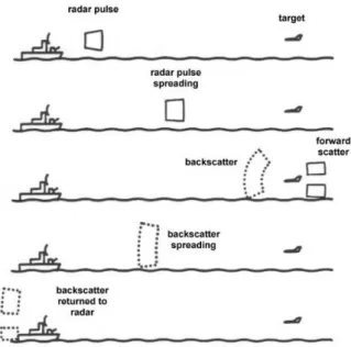
The electronic principle on which radar operates is very similar to the principle of sound-wave re‡ection. When shouting in the direction of a sound-re‡ecting object, there comes an echo. According to the speed of sound in air, one can estimate the distance and general direction of the object. The time required for an echo to return can be roughly converted to distance if the speed of sound is known. Radar uses electromagnetic energy in much the same way. The radio-frequency (RF) energy is transmitted to and re‡ected from the re‡ecting object. A small portion of the re‡ected energy returns to the radar set. This returned energy is called an echo, just as it is in sound terminology. Radar sets use the echo to determine the distance of the re‡ecting object.
Rmax= PtG2 2 (4 )3P min 1 4 (1.1) Radar system will obey the radar equation in Eq 1.1[1]. It represents the physical dependences and one can access the performance of the radar with the radar equation. First, we assume that electromagnetic waves propagate under ideal conditions. If RF energy is emitted by an isotropic radiator, than the energy propagate uni-formally in all directions. Areas with the same power density therefore form spheres (A= 4 R) around the radiator. Then in Fig. 1-1 it shows that target can be treat as another antenna. RF energy it re‡ected also propagate uni-formally. And how much it re‡ect can be replace by a coe¢ cient “ ”, Radar Cross Section (RCS). The used antenna play the role of transmitting and receiving. So antenna gain (G) should be square. And then, when transmitted larger power, the re‡ection power comes higher. Finally, the system sensitivity will decide the detection of rangeradar system.
Figure 1-1: Diagram of Radar System
After the introduction of radar system basic principle, we will introduce some di¤erent kinds of radar system. There are many di¤erent technologies for Anti-collision Safety System such as Ultra-sonic, Infrared, Laser, Video and Microwave radar. Microwave radar performs well in every items. So we choose it to implement our anti-collision system. In microwave radar system, there are also several di¤erent kinds. Such as pulse radar, FMCW radar and Doppler radar[2]. Pulse radar is popular in war time and has been well developed. Fig. 1-2(a) is a simple diagram of how pulse radar works. Generate several RF pulse signals, and …nd out in which time slot the recievied signal is. The distance resolution depends on how narrow in time domain the RF pulse is. Relative velocity can be found in the Doppler e¤ect on RF carrier. The algorithm of pulse radar is quite simple, but implementation of the circuit is much more di¢ cult then FMCW radar.
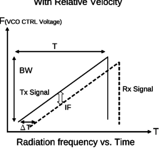
Fig. 1-2(b) is the diagram of FMCW radar. FMCW is the abbreviation of Frequency Modulation Continuous Wave. We add a linear frequency modulation on the center frequency. Fig. 1-3, Fig. 1-4 is voltage control oscillator (VCO) control voltage versus
to time. The time delay between transmitted signal (Tx) and received signal (Rx) will result in a inter-medium frequency (IF) signal. By detecting the IF signal frequency, we can calculate the target distance. Fig. 1-3 is the situation without relative velocity and Fig. 1-4 is with relative velocity. The IF signal is the result of distance and relative velocity. Relative velocity causes the Doppler e¤ect and will shit the IF frequency higher or lower. Doppler e¤ect will cause another problem in detection.
Doppler radar is similar to FMCW radar. Since relative velocity will cause some frequency shift. Transmit continuous wave (CW) and detect the frequency di¤erence between transmitted and recieved signal can get the relative velocity.
Target Target
(a) Target (b) Target
(a) (b)
Figure 1-2: (a) Pulse Radar Diagram (b) FMCW Radar diagram
T F(VCO CTRL Voltage)
Radiation frequency vs. Time
IF No Relative Velocity Rx Signal Tx Signal ΔT BW T T F(VCO CTRL Voltage)
Radiation frequency vs. Time
IF No Relative Velocity Rx Signal Tx Signal T F(VCO CTRL Voltage)
Radiation frequency vs. Time
IF No Relative Velocity Rx Signal Tx Signal ΔT BW T
T F(VCO CTRL Voltage)
Radiation frequency vs. Time
IF
With Relative Velocity
Rx Signal Tx Signal ΔT BW T T F(VCO CTRL Voltage)
Radiation frequency vs. Time
IF
With Relative Velocity
Rx Signal Tx Signal ΔT BW T T F(VCO CTRL Voltage)
Radiation frequency vs. Time
IF
With Relative Velocity
Rx Signal Tx Signal
ΔT
T F(VCO CTRL Voltage)
Radiation frequency vs. Time
IF
With Relative Velocity
Rx Signal Tx Signal
T F(VCO CTRL Voltage)
Radiation frequency vs. Time
IF
With Relative Velocity
Rx Signal Tx Signal
ΔT
BW T
Figure 1-4: Frequency Modulation Wave and Receiving Signal without Relative Velocity
1.3
FMCW Radar Distance and Velocity Detection
In FMCW radar, the IF frequency is proportional to the target distance if there is no relative velocity. So, distance resolution is decided by IF frequency resolution. In Fig. 1-3(a) is the condition without relative velocity. T is the period of control voltage. BW is the bandwidth of frequency modulation. It has 150 points in one cycle, so sample rate is 150T . VCO frequency slope “ ” is BWT and if the slope larger the IF frequency comes higher. From Eq 1.2 to Eq. 1.5. we can see that distance resolution is proportional to the used bandwidth and the ratio of over-sampling.
IF f requency = T / d (1.2)
M inimum F requency Resolution = 150 T 1 128 (1.3) so d = BW T d/ 150 T 1 128 (1.4)
Distance Resolution / BW (1.5) Velocity detection is according to Doppler e¤ect. Since Doppler e¤ect is fDoppler = 2vfC
only dependent on the operation frequency and relative velocity. Because IF frequency is the combination of distance and velocity, the control voltage slope rate should be higher enough. Doppler e¤ect in FMCW radar system will be discussed later.
Chapter 2
24GHz FMCW Radar System
2.1
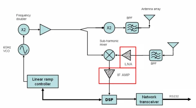
24GHz FMCW Radar System Architecture
Fig. 2-1 is the 24GHz FMCW radar system architecture. It can be separate into two parts. One is the RF circuit module and another is the IF ampli…er, frequency modulation control circuit and DSP core. First in RF circuit , there is a 6GHz VCO source and the tuning range should larger then the operation bandwidth. After VCO is a 6GHz to 12GHz frequency doubler and 12GHz ampli…er. In order to lower the e¤ect of antenna, two antenna type is chosen. One for transmitting signal and another for receiving the echo. After 12GHz ampli…er is a power divider which transmits the signal to Tx and Rx. In Tx path, there is a 12GHz to 24GHz frequency doubler, a band-pass …lter and a patch antenna for easy integration with other circuit. In Rx path, there is another 12GHz ampli…er to generate a ‡at LO signal. Next to the 12GHz ampli…er is a sub-harmonic mixer, band-pass …lter and patch antenna. LNA is the following work.
The base band circuits are IF ampli…er, frequency modulation control circuit and DSP core. IF ampli…er provides voltage gain and is an active band-pass …lter also. Frequency modulator is combined with DSP core in the micro-processor unit (MCU) we used. Combination of these two part can suppress timing error.
RS232 LNA IF AMP RS232 LNA IF AMP
Figure 2-1: 24GHz FMCW Radar System Architecture
2.2
24GHZ FMCW Radar System Algorithm
2.2.1
Signal Processing Flow Chart
Fig. 2-2 is the signal processing ‡ow chart of 24GHz FMCW radar system. It implements in ARM7 base microprocessor with 64KB RAM. Peripherals initial at the beginning. Set system clock to 40MHz to drive this chip in the highest performance. Then initiate peripherals such as:
1.AD/DA : For frequency modulation and sampling IF signal
2.Timer : Interrupt timer is to control AD/DA in the correct timing. 3.UART : Use it to transport data and change system parameter. 4.GPIO : Transport other control data such as LED alarm.
Initial Vt_gen & Sample Chirp Transform After Mask Target Est Alarm & Re-detection Initial Vt_gen & Sample Chirp Transform After Mask Target Est Alarm & Re-detection
Figure 2-2: FMCW Radar Digital Signal Flow Chart
The timer counts down and interrupts system into interrupt subroutine after initial-ization. Fig. 2-3 is the C code of interrupt subroutine. One key point should notice. The timing of resetting timer counter is important. Since the subroutine doesn’t spend the same operation time, the timer should be reset at the beginning (T1CLRI = 0). Other C code is to generate frequency modulation wave by changing register DAC0DAT and reading register ADCDAT to get IF signal.
Interrupt Subroutine T1CLRI = 0; DAC0DAT =(_Vtune[FIQ_times]<<16 ); ADCCON = 0x7E3; while (!ADCSTA){} _Sample_data[FIQ_times]=ADCDAT>>16; FIQ_times++;
Put those data into Chirp Transform and ignore the head and tail sample data to avoid transient distortion.. In the next section, there is some introduction of Chirp Transform and how to implement in C code. After Chirp Transform is a block call “After Mask”. As we all know, every system has its own noise. The way to design whether this result is a target or not is to compare the IF signal and background noise in frequency domain. In FMCW radar algorithm, a target makes an echo and results in a tone in frequency domian. We calibrate back ground noise and generate a threshold called “ Mask “. The detection result in frequency domain will compare with this threshold. The comparison result transports to the block “ Target Estimation”
Target Estimation is consisted of several determinations. The lower threshold is used the farer this system can detect. What happens if the threshold comes lower? There comes more un-wanted noise peak higher then the threshold. The determinations can …lter out some un-wanted noise and lower the threshold.
The result of target estimation is a …nal target table. The alarm condition has been decided at the beginnig and the micro-processor will generate alarm or start another detection according to those condition. In Fig. 2-1 some debug data will transport using UART. Once the radar is set at the testing car, it is hard to get the data in memory. So there is a simple communication protocol to communicate with radar system using UART.
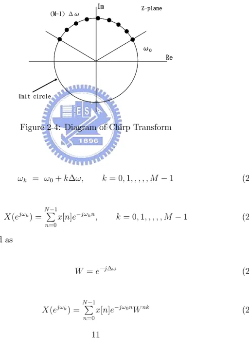
2.2.2
Chirp Transform
Chirp Transform (Fig. 2-4) is the extension of the DFT[3]. It is not optimal in minimizing any calculation, but is more ‡exible than the FFT. Un-like the FFT, the DFT is that multiply every data with the mapping coe¢ cient. Then the sum of all those multiply result is the value in frequency domain. Chirp Transform is quite the same as DFT. By modifying the coe¢ cients only part of points in unit circle are computed. Eq. 2.1 to Eq. 2.8 are the equations of Chirp Transform.
Re Im Z-plane ω0 (M-1) Δω Unit circle Re Im Z-plane ω0 (M-1) Δω Unit circle
Figure 2-4: Diagram of Chirp Transform
!k = !0+ k !; k = 0; 1; ; ; ; ; M 1 (2.1) X(ej!k) = NP1 n=0 x[n]e j!kn; k = 0; 1; ; ; ; ; M 1 (2.2) with W de…ned as W = e j ! (2.3) X(ej!k) = NP1 x[n]e j!0nWnk (2.4)
To express X(ej!k) as a convolution, we use the identity nk = 1 2 n 2+ k2 (k n)2 (2.5) X(ej!k) = NP1 n=0 x[n]e j!0nWn22 Wk22 W (k2n)2 (2.6) Letting g[n] = x[n]e j!0nWn22 (2.7)
We can then write
X(ej!k) = Wk22 (
NP1 n=0
g[n]W (k2n)2); k = 0; 1; ; ; ; ; M 1 (2.8)
The received signal frequency is start from DC so !0 is zero and simpli…es the C
code. Calculate the coe¢ cient (nk) …rst and …nd the mapping cosine and sine wave index. There is a natural back ground noise in low frequency. In order not to a¤ect higher frequency by the skirt of back ground noise, sample data should apply window on it. We choose Blackman Window since it has the lowest skirt level. Then multiply those after window data with W and add the results together. There is a shift n-bit operation in this C code. Because the micro-processor only calculates integer and in order not to be over-‡oat, pre-shift operation is necessary. Fig. 2-5 is part of Chirp Transform in C code.
for (n=0 ; n<128 ; n++) { nk=n*k; index_temp=(nk>>8); After_window= (*psample_data*Blackman_window[n-64])>>10; real+=After_window*(sin[index]); image+=After_window*(cos[index]); psample_data++; } . . real=(real>>12); image=(image>>12); _Chirp_result[k]=(real*real+image*image)>>1;
Figure 2-5: C Code of Chirp Transform
2.2.3
UART Protocol
There is a UART communication in the program for debuging this system. There are two things should notice. One is to make sure the communication link can built and the data in package should read correctly. Second is that this debug program should not a¤ect the main processing. If the terminator (PC with Labview) doesn’t plug on, this UART program should be bypassed. Under these two consideration, we design the following UART protocol as in Fig. 2-1. It is simple and can make sure the link is built. Also, it can bypass the UART program if the terminator doesn’t plug on.
Radar Detection Unit PC with LABVIEW Send Start Code Listening for Start Code
Send ACK if get Start Code Send ACK back if get ACK
Get Control Code and Send Data
Send Control Code if get ACK
Start Code ACK ACK Control Code
Data
Radar Detection Unit PC with LABVIEW Send Start Code Listening for Start Code
Send ACK if get Start Code Send ACK back if get ACK
Get Control Code and Send Data
Send Control Code if get ACK
Start Code ACK ACK Control Code
Data
Radar Detection Unit PC with LABVIEW Send Start Code Listening for Start Code
Send ACK if get Start Code Send ACK back if get ACK
Get Control Code and Send Data
Send Control Code if get ACK
Start Code ACK ACK Control Code
Data
Figure 2-6: Protocol of UART
Fig. 2-6 is the diagram of UART protocol. The terminator is in listenning mode at the beginning. When start up the debug program, micro-processor send a start code and wait for a short time. If there comes back an ACK, it send an ACK back. Then terminator transmits the control code. Control code can choose which data to read, such as sample data and Chirp Transform result. Control code can also change some parameters in radar system, such as frequency modulation range.
Chapter 3
Improvement of Radar system
3.1
Previous Approach in Algorithm (2D-FFT)
The previous approach is to generate 70 continuous triangular control waves. Since there is some transience and distorts the receiving data, we ignore the beginning ramps. Each triangular control wave has 150 sample points to avoid the transience at the head and tail of control wave. Choose 128 points each control wave and put into FFT with Hanning window. So we can get 64 FFT results just as showed in Fig. 3-1. Then take 64 FFT results into FFT again (Fig. 3-2). In …rst FFT, we acquire the information of distance. In second FFT, Doppler e¤ect can be separated out.
The trick of this approach is that after operating the …rst FFT, the results have amplitude and phase information. Since Doppler e¤ect presents on phase, the phase of the received signal can acquire the Doppler frequency. Common mode noise results in DC tern in 2D-FFT and a moving target can easily detected.
There are some defects of this approach. First it needs a lot of computation. In this setting, it requires 128 points FFT x 64 times and 64 points FFT x 128 times to get hole 2D spectrum result. Second is the common mode noise will blank the static target. Third is that in order to avoid Doppler e¤ect which distorts the distance information, control wave frequency should higher enough. Doppler e¤ect makes receiving signal shift
in frequency domain and the shift level is proportional to relative velocity and operation frequency. In order to bear higher relative velocity, the control voltage slope comes larger. In the setting, frequency resolution is 150128T1 and Doppler e¤ect should less then a frequency resolution. Since this radar system implements in an imbedded system, smaller T not only needs a faster AD/DA but also increases the cost of this system.
T F(VCO CTRL Voltage)
Radiation frequency vs. Time
Ramp1 Ramp2 75 Ramps 128 points FFT FFT2 FFT1 T T F(VCO CTRL Voltage)
Radiation frequency vs. Time
Ramp1 Ramp2 75 Ramps 128 points FFT FFT2 FFT1 T
Figure 3-1: First FFT Operation
T F(VCO CTRL Voltage)
Radiation frequency vs. Time
64 Ramps FFT2 FFT1 FFT3 FFT4 64 points FFT 128 points T T F(VCO CTRL Voltage)
Radiation frequency vs. Time
64 Ramps FFT2 FFT2 FFT1 FFT1 FFT3 FFT3 FFT4 FFT4 64 points FFT 128 points T
3.2
New Approach in Algorithm
3.2.1
Triangular Control Wave
In previous approach, there should have a fast AD/DA, large RAM size and a DSP core to calculate so many FFT points. Looking at the frequency modulation wave in previous approach, it just uses the rising edge. What if we use a triangle modulation wave? In Fig. 3-3 is the new control wave and triangle shape has two side information. If the target is approaching to radar, Doppler e¤ect shift the receiving signal upward. If we call F1 as the frequency of rising part IF signal and F2 as the frequency of falling part IF signal, F1, F2 are di¤erent about two times Doppler frequency.
F 1 = Distance f requency Doppler f requency (3.1)
F 2 = Distance f requency + Doppler f requency (3.2) Plus F1 and F2 together can cancel Doppler e¤ect and F2 minus F1 can get two times of Doppler frequency. This simple change makes us to use Doppler e¤ect rather than to against it. There are some conclusions of this new approach. (1)It can easily cancel Doppler e¤ect. (2)Comparing F1, F2 can get the relative velocity and whether the target is approaching or not. (3)This approach can slow down AD/DA update rate. Because it doesn’t need to avoid Doppler e¤ect distortion but using it. (4)It can apply several decision condition to avoid noise. For example, rising part and falling part should detect the target at the same time. The frequency di¤erence between rising part and falling part should be limited in a range. It can ignore many random noise and lower the false alarm rate. (5)New approach only need twice 128 points FFT which saves a lot of memory and a slower micro-processor is enough.
T BW 150 sample points ( T ) ΔT Receive Signal Transmit Signal F(VCO CTRL Voltage) F1 F2 T BW 150 sample points ( T ) ΔT Receive Signal Transmit Signal F(VCO CTRL Voltage) F1 F2
Figure 3-3: Triangular Control Wave
3.2.2
Triangular Control Wave Test Result
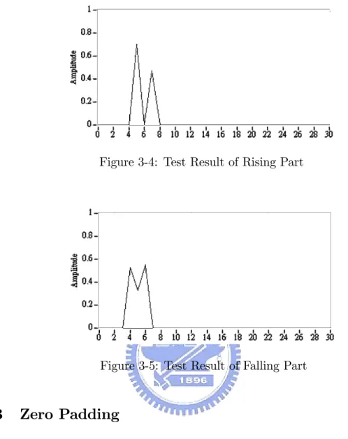
Fig. 3-43-5 are the test result of this triangular control wave. There is a moving car at the speed 10km/hr and the direction is away from the radar. In Fig. 3-43-5 there are two peak in the test result. That is because a car may have more then one re‡ection center and will result in multi-peaks in frequency domain. The test car is in the direction away from radar system and the test result of rising part of control wave will higher then falling part. Fig. 3-4 is the rising part and Fig. 3-5 is the falling part. It is easy to …nd that the result of rising part has one index more then the falling part. One index di¤erece means the relative velocity is about 10km/hr and is quite mach the test condition.
Figure 3-4: Test Result of Rising Part
Figure 3-5: Test Result of Falling Part
3.2.3
Zero Padding
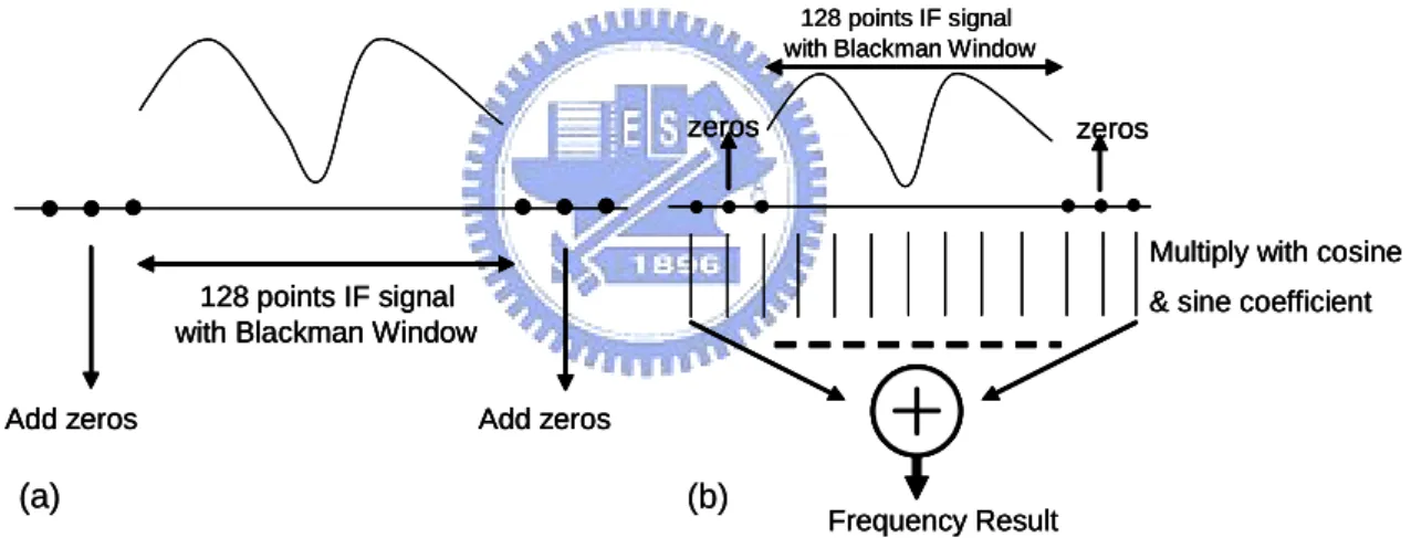
We know that distance resolution depends on the bandwidth. But according to FCC mask, only 200MHz bandwidth can be used. Ideally, 75cm is the natural limitation in distance resolution. What if we want the target position more precisely? In digital signal processing there is one way called “Zero Padding”. Under the same sampling rate and the same sample point, frequency resolution is already decided as sampling ratesample points. But we can …ll up the result between each frequency index by zero padding[4].
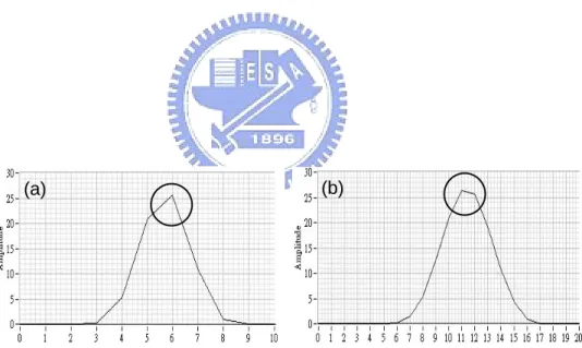
Zero padding is that add several zeros at the head and tail of the signal. In Fig. 3-6(a) is the diagram of zero padding. First generate a 5.7KHz 128 points sine wave signal (Fig. 3-7(a)). Apply Blackman window on this test signal and then adds 128
zeros (Fig. 3-7(b)). After FFT operation, the maximum value appears at 6KHz without zero padding. Using zero padding, the maximum value is at 5.5KHz. So the frequency resolution becomes two times better then normal FFT and distance resolution becomes two times better also. Fig. 3-8 is the simulation result.
Next step is to implement this approach in C code after the simulation of zero padding. Fig. 3-6(b) is the diagram of Chirp Transform calculation with zero padding. Add zeros at the head and tail of data as a new data. Then operate Chirp Transform on the new data set. Since Chirp Transform is more ‡exible then FFT, we can use some programming skill to lower the computation quantity. In Fig. 3-6(a), every data should multiply with a coe¢ cient and add together. Zeros also multiply and add together but they waste the computation resource. So, just change the …rst for loop of the C code in Fig. 2-5. Shift the start index from 0 to zero numbers then zero padding is easily implemented.
128 points IF signal with Blackman Window
zeros zeros
Multiply with cosine & sine coefficient
Frequency Result 128 points IF signal
with Blackman Window
Add zeros Add zeros
(a) (b)
128 points IF signal with Blackman Window
zeros zeros
Multiply with cosine & sine coefficient
Frequency Result
128 points IF signal with Blackman Window
zeros zeros
Multiply with cosine & sine coefficient
Frequency Result 128 points IF signal
with Blackman Window
Add zeros Add zeros
128 points IF signal with Blackman Window
Add zeros Add zeros
(a) (b)
Figure 3-6: (a) Diagram of Zero Padding (b)Diagram of Chirp Transform Calculation with Zero Padding
(a) (b)
(a) (b)
Figure 3-7: (a)128 points 5.7KHz sine waveform (b) Test Signal with Blackman Window and Zero Padding
(a) (b)
(a) (b)
Figure 3-8: (a) Without Zero Padding Frequency Result (b)With Zero Padding Frequency Result
3.3
Improvement in IF Ampli…er
There is a back ground noise in FMCW radar system naturally. Output power ‡atness will cause an AM modulation and result in a low frequency back ground noise. Self-mixing in mixer, antenna leakage and leakage wave in RF module will also result in a back ground noise. Fig. 3-9 is the IF signal under previous IF ampli…er and Fig. 3-10 is the FFT result. It is easy to …nd that back ground noise is in lower frequency.
Rising Part Falling Part Rising Part Falling Part
Figure 3-9: IF Signal in Previous IF Ampli…er
Since the wanted frequency is also start from DC, this overlap between back ground noise and wanted signal results in two problem. One is that back ground noise is too large and blinds the region near to radar. Second is that back ground noise limits IF ampli…er gain and makes system sensitivity poorer. Fig. 3-11 is the diagram of limitation in frequency domain. In region 1, back ground noise dominate the noise ‡oor. In region 2 and region 3 the skirt of back ground noise and quantization error consist the noise ‡oor. Region 2 is the previous detection region. Quantization error dominates the noise ‡oor in region 3 because the skirt of back ground noise is quite lower then in region 2. How can we suppress the quantization error noise?
1 2 3
1 2 3
Figure 3-11: Diagram of the Limitation in Frequency Domain
Back ground noise is the limitation of gain in previous IF ampli…er. But what if we move pole 1 to higher frequency. Fig. 3-12 is the frequency response of previous IF ampli…er and the new one. Using IF ampli…er as an active …lter. Higher pole1 can suppress back ground noise and lower pole2 can …lter out aliasing and noise in higher frequency. Once the back ground noise has been suppressed, higher IF ampli…er gain is admitted. Signal in region 3 ampli…es to higher voltage and improves the signal to noise ratio. Fig. 3-13 are the test result and a diameter in 15cm iron tube is the target. Fig. 3-13(a) is the result using previous IF ampli…er frequency response and Fig. 3-13(b)
is the result of new one. The farest detection distance moves up to 17m and system sensitivity improves about 10dB. This new IF ampli…er provides higher gain and noise ‡oor in region 3 dominates by RF module.
F Gain
F Gain
(a) Previous Amp FR (b) New Amp FR
pole1 pole2 pole1 pole2 F Gain F Gain
(a) Previous Amp FR (b) New Amp FR
F Gain
F Gain
(a) Previous Amp FR (b) New Amp FR
pole1 pole2
pole1 pole2
Figure 3-12: (a) Frequency Response of Previous IF Ampli…er (b) Frequency Response of New IF Ampli…er
Rising Part Falling Part Rising Part Falling Part
(a) (b)
Rising Part Falling Part Rising Part Falling Part
(a) (b)
Figure 3-13: (a) Test Result with Previous IF Ampli…er (b) Test Result with New IF Ampli…er
Chapter 4
6GHz Compact Size FMCW Radar
System
We try to built a compact size 6GHz FMCW radar system base on the experience in 24GHz FMCW radar. In 24GHz FMCW radar, there are two antennas to lower the interaction between Tx path and Rx path. And since it is built by discrete component, it’s hard to generate a 24GHz source directly. So there comes two frequency doubler and more RF circuit make the module size larger.
In 6GHz FMCW radar system, we try to use as less components as possible. There is only a 6GHz VCO, a 90 hybrid mixer and uses one antenna for both Tx and Rx. Fig. 4-1 is the block diagram of compact size 6GHz FMCW radar system RF module. In the following article, we will have some discussion on antenna, mixer, …lter and VCO. First is two di¤erent antenna types. One is a compact size novel wideband antenna and another is a 2 x 1 antenna array using aperture couple antenna.
6GHz VCO To IF Amp 6GHz Hybrid Mixer TX Rx LPF 6GHz VCO To IF Amp 6GHz Hybrid Mixer TX Rx LPF
Figure 4-1: 6GHz Compact Size FMCW Radar Block Diagram
4.1
Novel Wideband Antenna Con…guration
Recently there is tremendous demand for the development of wireless communication systems or mobile phone system. In order to have compact size device, several antenna structures with small dimension are proposed. Inverted-F antenna is a common structure. One shorted end makes it only quarter wavelength. This structure can provide E-plane and H-plane current path make its radiation pattern more omni-direction.
In order to integrate with other circuit, printed inverted-F structure is proposed (Fig. 4-2)[5]. In Fig. 4-2 there is a big gap G in traditional printed inverted-F antenna. What if we reduce the gap size ? Lower the gap size and move the antenna quite close to the ground plane can highly improve antenna bandwidth. So in the article, we propose a wideband antenna structure with small gap proximity to ground plane and will discuss several parameters and their e¤ect.
Via
G Via
G
Figure 4-2: Con…guration of Inverted-F Antenna
4.1.1
Antenna structure and Parameter discussion
When designing an antenna, we should consider not only how much area antenna has but also the ground plane size. In this antenna we decide to use on a dungo size device. So the ground plane we choose is 20mm x27mm. Fig. 4-3 illustrates the geometry of this investigated antenna. It is printed on 0.8mm FR4 with micro-strip line feed. The area of the antenna is 19mm x 11.5mm ((L1+L2) x H), ground plane is 20mm x 27mm with the gap (G) 0.8mm and there is a via short to ground plane. Next we will discuss the e¤ect of several parameters and all those comparisons are simulated in HFSS 8.0.
L1 L2 Via G H 27mm 20mm Y X L1 L2 Via G H 27mm 20mm Y X Y X
First separate this wideband antenna structure into two part. One is the main radiator at the right side. Another is a short end at the left. The main radiator in Fig 4-4 is just like a monopole antenna serial with one transmission line. But the transmission line doesn’t lie right on the ground plane. So it has high impedance an will generate some radiation. Comparing these two antenna structures we can …nd out that add this radiant transmission line can highly improve return loss bandwidth (Fig. 4-5).
(a) (b)
(a) (b)
Figure 4-4: (a) Right Part of Wideband Antenna with Radiant Transmission Line (b) Right Part of Wideband Antenna without Radiant Transmission Line
1 3 5 7 9 Frequency (GHz) -40 -30 -20 -10 0 Return Gain (dB) Ant b Ant a 1 3 5 7 9 Frequency (GHz) -40 -30 -20 -10 0 Return Gain (dB) Ant b Ant a
Fig. 4-6 demonstrates the simulated result in di¤erent gap distance (G). This the new wideband antenna is similar to traditional inverted-F but the gap proximity to ground plane is di¤erent. In order not to change the lowest frequency, we keep total length (L1+L2+H+G) as constant. We choose several gap values from 4 mm to 0 mm. When G becomes smaller, the e¤ect become stronger. By changing G the bandwidth become wider and there comes a new deep in higher frequency. In here G=0.5mm has the widest bandwidth. 1 3 5 7 9 Frequency (GHz) -40 -30 -20 -10 0 G=0.5 G=1 G=4 G=0 Return Gain (dB) 1 3 5 7 9 Frequency (GHz) -40 -30 -20 -10 0 G=0.5 G=1 G=4 G=0 Return Gain (dB)
Figure 4-6: Simulated Result of G from 0mm to 4mm
In Fig. 4-7 we change H and …nd out that the deep locations change. Since this antenna can be treat as a monopole with two matching transmission line. The length H just like a monopole antenna load. When H becomes larger, frequency becomes lower. Since L1, L2 and G keep un-changed, the matching circuit is the same.
Fig. 4-8 shows the relationship between L1 and return lose. We choose several L1 values from 4.5mm to 9mm and the band-width doesn’t change much but shift to lower frequency when L1 is shorter. At the beginning, we seperate this antenna into two part. The wideband mechanism is a monopole with a radiate transmission line and L1 is a matching circuit which makes the bandwidth wider.
1 3 5 7 9 Frequency (GHz) -40 -30 -20 -10 0 Return Gain (dB) H=11.5 H=12.5 H=13.5 H=10.5 1 3 5 7 9 Frequency (GHz) -40 -30 -20 -10 0 Return Gain (dB) H=11.5 H=12.5 H=13.5 H=10.5
Figure 4-7: Simulated Result of H from 10.5mm to 13.5mm
1 3 5 7 9 Frequency (GHz) -40 -30 -20 -10 0 Return Gain (dB) L1=6 L1=7.5 L1=9 L1=4.5 1 3 5 7 9 Frequency (GHz) -40 -30 -20 -10 0 Return Gain (dB) L1=6 L1=7.5 L1=9 L1=4.5
Figure 4-8: Simulated Result of L1 from 4.5mm to 9mm
locations and bandwidth. In the next several Smith Chart (Fig. 4-10 Fig. 4-11 ), we put di¤erent L2 simulation results into Smith Chart to …nd out how L2 e¤ect. When L2 become smaller, it pulls the S-parameter closer to center. At the same G size, L2 is a critical part of wideband matching.
1 3 5 7 9 Frequency (GHz) -40 -30 -20 -10 0 Return Gain (dB) L2=7.5 L2=8.5 L2=9.5 L2=6.5 1 3 5 7 9 Frequency (GHz) -40 -30 -20 -10 0 Return Gain (dB) L2=7.5 L2=8.5 L2=9.5 L2=6.5
Figure 4-9: Simulated Result of L1 from 6.5mm to 9.5mm
0 1.0 1.0 -1.0 10.0 10.0 -10.0 5.0 5.0 -5.0 2.0 2.0 -2.0 3.0 3.0 -3.0 4.0 4.0 -4.0 0.2 0.2 -0.2 0.4 0.4 -0.4 0.6 0.6 -0.6 0.8 0.8 -0.8 Swp Max 9GHz Swp Min 1GHz L2_6.5mm 0 1.0 1.0 -1.0 10.0 10.0 -10.0 5.0 5.0 -5.0 2.0 2.0 -2.0 3.0 3.0 -3.0 4.0 4.0 -4.0 0.2 0.2 -0.2 0.4 0.4 -0.4 0.6 0.6 -0.6 0.8 0.8 -0.8 L2_7.5mm Swp Max 9GHz Swp Min 1GHz 0 1.0 1.0 -1.0 10.0 10.0 -10.0 5.0 5.0 -5.0 2.0 2.0 -2.0 3.0 3.0 -3.0 4.0 4.0 -4.0 0.2 0.2 -0.2 0.4 0.4 -0.4 0.6 0.6 -0.6 0.8 0.8 -0.8 Swp Max 9GHz Swp Min 1GHz L2_6.5mm 0 1.0 1.0 -1.0 10.0 10.0 -10.0 5.0 5.0 -5.0 2.0 2.0 -2.0 3.0 3.0 -3.0 4.0 4.0 -4.0 0.2 0.2 -0.2 0.4 0.4 -0.4 0.6 0.6 -0.6 0.8 0.8 -0.8 Swp Max 9GHz Swp Min 1GHz L2_6.5mm 0 1.0 1.0 -1.0 10.0 10.0 -10.0 5.0 5.0 -5.0 2.0 2.0 -2.0 3.0 3.0 -3.0 4.0 4.0 -4.0 0.2 0.2 -0.2 0.4 0.4 -0.4 0.6 0.6 -0.6 0.8 0.8 -0.8 L2_7.5mm Swp Max 9GHz Swp Min 1GHz 0 1.0 1.0 -1.0 10.0 10.0 -10.0 5.0 5.0 -5.0 2.0 2.0 -2.0 3.0 3.0 -3.0 4.0 4.0 -4.0 0.2 0.2 -0.2 0.4 0.4 -0.4 0.6 0.6 -0.6 0.8 0.8 -0.8 L2_7.5mm Swp Max 9GHz Swp Min 1GHz Figure 4-10: L2=6.5mm & L2=7.5mm 0 1.0 1.0 -1 .0 10.0 10.0 -10.0 5.0 5.0 -5 .0 2.0 2.0 -2 .0 3.0 3.0 -3 .0 4.0 4.0 -4 .0 0.2 0.2 -0.2 0.4 0.4 -0.4 0.6 0.6 -0 .6 0.8 0.8 -0 .8 L2_8.5mm Swp Min 1GHz Swp Max 9GHz 0 1.0 1.0 -1 .0 10.0 10.0 -10.0 5.0 5.0 -5 .0 2.0 2.0 -2 .0 3.0 3.0 -3 .0 4.0 4.0 -4 .0 0.2 0.2 -0.2 0.4 0.4 -0.4 0.6 0.6 -0 .6 0.8 0.8 -0.8 Swp Max 9GHz Swp Min 1GHz L2_9.5mm 0 1.0 1.0 -1 .0 10.0 10.0 -10.0 5.0 5.0 -5 .0 2.0 2.0 -2 .0 3.0 3.0 -3 .0 4.0 4.0 -4 .0 0.2 0.2 -0.2 0.4 0.4 -0.4 0.6 0.6 -0 .6 0.8 0.8 -0 .8 L2_8.5mm Swp Min 1GHz Swp Max 9GHz 0 1.0 1.0 -1 .0 10.0 10.0 -10.0 5.0 5.0 -5 .0 2.0 2.0 -2 .0 3.0 3.0 -3 .0 4.0 4.0 -4 .0 0.2 0.2 -0.2 0.4 0.4 -0.4 0.6 0.6 -0 .6 0.8 0.8 -0 .8 L2_8.5mm Swp Min 1GHz Swp Max 9GHz 0 1.0 1.0 -1 .0 10.0 10.0 -10.0 5.0 5.0 -5 .0 2.0 2.0 -2 .0 3.0 3.0 -3 .0 4.0 4.0 -4 .0 0.2 0.2 -0.2 0.4 0.4 -0.4 0.6 0.6 -0 .6 0.8 0.8 -0.8 Swp Max 9GHz Swp Min 1GHz L2_9.5mm 0 1.0 1.0 -1 .0 10.0 10.0 -10.0 5.0 5.0 -5 .0 2.0 2.0 -2 .0 3.0 3.0 -3 .0 4.0 4.0 -4 .0 0.2 0.2 -0.2 0.4 0.4 -0.4 0.6 0.6 -0 .6 0.8 0.8 -0.8 Swp Max 9GHz Swp Min 1GHz L2_9.5mm Figure 4-11: L2= 8.5mm & L2= 9.5mm
From the comparison before, we know that monopole with radiant transmission line is naturally a wideband structure. Now we just simulate the right part of novel wideband antenna and only change the gap size. In Fig. 4-12 when gap is precisely chosen, the bandwidth can be quite large to about 2GHz. There is a deep in higher frequency and is caused by the discontinuity of antenna.
Base on this wideband structure, we propose a wideband antenna with its bandwidth from 3.1GHz to more the 9GHz. Antenna size is 14.6mm x 10mm ((L1+L2) x H). The main radiator is like a triangle. It can provide longer and di¤erent current path for lower frequency. Then use radiant transmission line for wideband purpose. Use the short end to smaller the size to quarter wavelength and be the …nal matching too. By tuning those parameters we have this wideband antenna in such a small size. Fig. 4-13 is the structure of this wideband antenna and Fig. 4-14 is the measurement return gain of it.
1 3 5 7 9 Frequency (GHz) -40 -30 -20 -10 0 Return Gain (dB) G=0.5 G=1 G=4 G=0 1 3 5 7 9 Frequency (GHz) -40 -30 -20 -10 0 Return Gain (dB) G=0.5 G=1 G=4 G=0
Via H L1+L2 Y X Via H L1+L2 Via H L1+L2 Y X Y X
Figure 4-13: Novel Wideband Antenna Structure
2 4 6 8 10 12 Frequency (GHz) -40 -30 -20 -10 0 Return Gain ( dB) 2 4 6 8 10 12 Frequency (GHz) -40 -30 -20 -10 0 Return Gain ( dB)
Figure 4-14: Return Gain of Wideband Antenna
4.1.2
Antenna Pattern
There are the radiation patterns in 3.5GHz and 7.5GHz. Main radiator has a radiation pattern similar to a monopole and the transmission line (L1+L2) which proximity to the ground compensates some null in radiation pattern. With this radial transmission line, the total …eld becomes more omni direction. When the frequency becomes higher that transmission line generates more radiation. In 7.5GHz the antenna gain is smaller then zero. This may causes by the loss of fr4.
(a) (b)
(a) (b)
Figure 4-15: (a) XZ plane in 3.5GHz (b) YZ plane in 3.5GHz
(a)
(b)
(a)
(b)
Figure 4-17: (a) XZ plane in 7.5GHz (b) YZ plane in 7.5GHz
4.2
Aperture Couple Antenna Array
In chapter 4.1 is a wideband antenna structure. It has an omni-direction radiation pattern but in some application the radiation pattern should be more directivity. In this section, we propose a aperture couple antenna array. This can avoid some re‡ection from the un-wanted region such as ground plane.
4.2.1
Aperture Couple Antenna Array Con…guration
Fig. 4-19 is the structure of this antenna array[6]. Fig. 4-19(a) is the slot and the feed line. Fig. 4-19(b) is the main radiator. Fig. 4-20 is the sight draft of this antenna array. Total size is 46mm x 70mm x 5mm (W x L x H) and uses 0.4mm fr4. The feed line excites the the radiator through the aperture. Once the operation frequency is decided, the size of the main radiator also decided. The over length of the feed line is used to tune the matching and the length and width of slot also e¤ect the matching. The main radiator is about /4 of the operation frequency and the distance between two radiator is /2. Aperture couple antenna has narrower beam width then normal patch antenna, so two antenna elements is enough.
L W (a) Y (b) X L W (a) (b) L W (a) Y (b) X Y X
Figure 4-19: (a) The Lower Part of Array (including feed line and slot) (b) The Upper Part of Array
Upper Layer FR4 Air (H) Slot FR4 Feed Upper Layer FR4 Air (H) Slot FR4 Feed Figure 4-20: Sight Draft of Antenna Array
4.2.2
Return Gain and Antenna Pattern
This aperture couple antenna array has 400MHz bandwidth from 5.8GHz to 6.2GHz. Half power beam width in XZ plane is 42 and peak gain is10.8dBi.
4 5 6 7 8 Frequency (GHz) -40 -30 -20 -10 0 Return Gain (d B) 4 5 6 7 8 Frequency (GHz) -40 -30 -20 -10 0 Return Gain (d B)
Figure 4-22: Aperture Couple Antenna Array Radiation Pattern in XZ and YZ plane
4.3
Compact Size Low-pass Filter
In Fig. 4-1, there is a low-pass …lter after the hybrid mixer to …lter out all harmonic frequencies generated by the circuit. In this radar structure there only needs a low-pass …lter not a band-pass …lter to …lters out VCO fundamental frequency. So a low-pass …lter with zeros at 12GHz and 18GHz is enough and that makes the circuit in small size. Fig. 4-23(a) is the layout of this …lter and Fig. 4-23(b) is the equivalent circuit. Total size is 4.6mm x 3.2mm (L x W) on 20mil RO4003. There comes two zeros. One is the parallel inductor with couple capacitor. Another is the serial inductor with capacitor to ground. The equivalent circuit is a common type of low-pass …lter[7]. Fig. 4-24 is the measurment result. There is one pole near 12GHz to …lter out second harmonic frequency and another pole is at 17GHz. Although we want to put the …rst pole at 12GHz and the next pole at 18GHz these two poles have interaction and is hard to modify them indepently.
L
W
(a)
(b)
L
W
L
W
(a)
(b)
Figure 4-23: (a) Lowpass Filter Layout (b) Filter Equivalent Circuit
4 8 12 16 20 Frequency (GHz) -40 -30 -20 -10 0 S11 S21 4 8 12 16 20 Frequency (GHz) -40 -30 -20 -10 0 S11 S21
Figure 4-24: Lowpass Filter S parameter
4.4
Hybrid Mixer
Fig. 4-25(a) is the schematic of hybrid mixer[8]. It consists of a quadrature hybrid and two low barrier schottky diodes. The symmetrical structure can compensate the common mode noise. With high LO power and low barrier diode, there needs no extra bias network to improve the conversion loss. Because the Lo signal is far away from IF signal, it only needs a simple quarter open stub and a LC network to perform as a LPF. 90 hybrid splits the LO signal with equal amplitude and 90 phase di¤erence to mixing
diodes. These signals are re‡ected and combine at the antenna port. The insertion loss of this hybrid mixer is the summation of re‡ection loss from diode and hybrid loss. The received signal also splits by this 90 hybrid. The IF signal comes 180 phase di¤erence and a operational ampli…er is used as a balun and active …lter.
IF IF IF IF (a) (b) (c) (d) IF IF IF IF IF IF IFIF IF IF IF (a) (b) (c) (d)
Figure 4-25: (a) Normal Hybrid Mixer (b) Hybrid Mixer with Short Stub (c) Hybrid Mixer with Open Stub (d) Hybrid Mixer with Filter
4.4.1
Hybrid Mixer Improvement and Test Result
In basic hybrid mixer structure it has 1.7 dB insertion loss and 12 dB conversion loss. Is there any approach to improve the performance without increasing too much area? There are some papers[9][10] discussing the improvement of conversion loss. We can have a conclusion that at each port (LO port, RF port and IF port) if the wanted frequency can pass and the un-wanted frequency is re‡ected, this will be an optimum conversion loss mixer.
IF port has a LPF and quarter wave stub in hybrid mixer so LO signal and RF signal can’t through. RF port and LO port are the same and should re‡ect the un-wanted signal. To achieve this purpose, we try to add some stub or …lter at RF port. Fig. 4-25 is the schematic of hybrid mixer. There are some di¤erent types; open stub, sort stub and compact size LPF. All those external circuits are used to re‡ect the second harmonic frequency back to the mixing diode. Fig. 4-26 is the comparison result and the comparison is base on 6dBm LO power as the condition this module is. And the test results arequite the same when changing the LO from 4dBm to 8dBm. There comes about 1 2dB improvement when add those stubs. In order to save more space, we choose the structure with open stub (type (c)) as the mixer in this radar module.
• Mixer type Insertion Loss Conversion Loss • Type (a) 1.7dB 12dB
• Type (b) 1.7dB 11.5dB • Type (c) 1.5dB 10dB
• Type (d) 1.3dB 11.3dB
4.5
Voltage Control Oscillator
For a BJT negative resistance oscillator the most e¤ective network is the common base con…guration[11]. An serial inductor from base to ground can easily generate negative resistance but it is for low output power use. In this radar module, we choose common emitter network to generate high output power. There is a open stub at the collector to obtain negative resistance. A micro-strip line and a varactor connects to the base as LC tank and derive the signal at the emitter. For better performance discrete components only use as bias and bypass. Fig. 4-27 is the schematic of this oscillator. Fig. 4-28 is the layout of this oscillator. Fig. 4-29 is the phase noise measurement result. It is -101 dBc/Hz @ 100KHz, -124dBc/Hz @ 1MHz and the output power is 12dBm.
Bias Network Output Varactor Bias Network Output Varactor
B E C C R R C R R C R C C Tank Bias Bias B E C C R R C R R C R C C Tank Bias Bias
Figure 4-28: VCO layout
Chapter 5
6GHz FMCW Radar System
Integration and Measurement
R R R VCO 5dB PAD Test Port Ant Port Mixer 6G Filter L L C R C R IF Filter I/O port R R R VCO 5dB PAD Test Port Ant Port Mixer 6G Filter L L C R C R IF Filter I/O port
Figure 5-1: RF Module Layout
Fig. 5-1 is the RF module layout of this Radar system. The dimension is 30mm x 50mm and implements on 20mil RO4003. The power consumption is less then 200mW under 5V supply voltage. There is a 5dB PAD after 6GHz VCO. Generally, There is an
ampli…er or a frequency multiplier next to oscillator. An ampli…er can not only enhance power to push the next stage but also be a bu¤er to avoid load pulling e¤ect. But to minimize circuit size, we use a 5dB pad to lower the load pulling e¤ect. Even we do so, mixer and VCO still need to be co-designed. After mixer is a low-pass …lter to suppress harmonic generated by mixer and VCO.
In Fig. 5-2 is the measurement result of this RF module. There is about 5dBm output power in the operation frequency range. The frequency sensitivity doesn’t perform well but we can modify the control voltage shape to make the output frequency linearer. Fig. 5-3 is the harmonic test result. All harmonic frequencies are suppressed more then 40dB. This means that …lter performs well.
73.4 5.52 6.0675 5 85 5.2 6.0308 4.5 101.6 5.22 5.9883 4 115 5.17 5.9375 3.5 100 5.18 5.88 3 93.4 5.28 5.83 2.5 90 5.45 5.7833 2 81.6 5.63 5.7383 1.5 73.4 5.78 5.6975 1 73.6 5.82 5.6608 0.5 5.82 5.624 0 Sensitivity (MHz/V) Output Power (dBm) Output Frequency (GHz) Vt (V) 73.4 5.52 6.0675 5 85 5.2 6.0308 4.5 101.6 5.22 5.9883 4 115 5.17 5.9375 3.5 100 5.18 5.88 3 93.4 5.28 5.83 2.5 90 5.45 5.7833 2 81.6 5.63 5.7383 1.5 73.4 5.78 5.6975 1 73.6 5.82 5.6608 0.5 5.82 5.624 0 Sensitivity (MHz/V) Output Power (dBm) Output Frequency (GHz) Vt (V)
Figure 5-3: RF Module Output Spectrum
Since the hybrid mixer has di¤erential IF output, an operational ampli…er is used as balun and active …lter. Fig. 5-4 is the schematic of IF ampli…er. In the previous section, system sensitivity can be better by changing pole1 and pole2. The ratio of input and feedback resistor decides the ampli…er gain and change the capacitors can modify pole position to …nd an optimum value. Fig. 5-5 is the test result of this 6GHz FMCW radar system. The target is an iron tube is 15cm diameter at 34.5m. NI DAQCard-6062E is used as the control wave generator and the ADC sampler. The frequency modulation bandwidth is 150MHz and the distance resolution is 1.2m ideally. Using zero padding technology the distance resolution upgrades to 0.3m. The detection result is at index 118 and the distance resolution is 0.29m. This is quite close to the expect result. Fig. 5-6 and Fig. 5-7 are the photographs of RF module and total system.
Pole1
Pole2
Pole1
Pole2
Figure 5-4: IF Ampli…er Schematic
Figure 5-6: 6GHz Radar RF Module Photograph
Chapter 6
Conclusion
This article provides a compact size 6GHz FMCW radar module. From antenna to RF circuit and digital signal processing are all included. Di¤erent kinds of antennas can be chosen according to di¤erent applications. RF module has low power consumption and low cost either. In digital signal processing there are some improvements base on the experience in 24GHz FMCW radar system.
Triangle modulation wave increases system stability and saves a lot of system resource. Chirp Transform is more ‡exible then FFT and is easy to implement zero padding tech-nology. The modi…ed IF ampli…er can increase system sensitivity about 10dB better and the detection range becomes two times farer then before.
The drawback of this radar system is the antenna size. The circuit performance is better in lower frequency and can accept more manufacturing torelance. But a radar system always needs high directivity and low operation frequency makes antenna larger. A compact size antenna with high directivity will be the future work.
Bibliography
[1] David M. Pozar;Microwave Engineering,3rded. :Wiley ,pp.661 [2] Skolnik, Merrill I.; Introduction to radar systems :McGraw-Hill
[3] Oppenheim, Alan V.;Schafer, Ronald W.; Discrete-time signal processing :Prentice Hall ,pp.656-661
[4] Qi Guoqing; “High accuracy range estimation of FMCW level radar based on the phase of the zero-padded FFT”, in ICOSP.2004, vol 3, 31 Aug.-4 Sept. 2004
[5] Zhu Qi, Fu Kan, Liang Tie-zhu; “Analysis of planar inverted-F antenna using equiv-alent models”, in APS.2005, vol. 3A, pp.142 - 145, 3-8 July 2005
[6] Jong Moon Lee; Won Kyu Choi; Cheol Sig Pyo; “RF integrated aperture coupled antenna for satellite communication at Ku-band”, in Antennas and Propagation Society International Symposium, 2003. IEEE, vol.4, pp. 702-705, 22-27 June 2003 [7] David M. Pozar;Microwave Engineering,3rded. :Wiley ,pp.401
[8] Tan Hsing Ho; Shyh Jung Chung; “A Compact Doppler Radar Using A New Hybrid Mixer”, in International Joint Conference of the 6th topic Symposium on Millimeter Wave TSMMW2004
[9] Madjar, A.; “A novel general approach for the optimum design of microwave and millimeter wave subharmonic mixers” in Microwave Theory and Techniques, IEEE
[10] Quan Xue; Kam Man Shum; Chi Hou Chan; “Low conversion-loss fourth subhar-monic mixers incorporating CMRC for millimeter-wave applications” in Microwave Theory and Techniques, IEEE Transactions, Vol 51, Issue 5, pp.1449 - 1454, May 2003
[11] Guillermo Gonzalez;Microwave Transistor Ampli…ers Analysis and Design,2nd