行政院國家科學委員會專題研究計劃成果報告
CMOS 發光顯像技術與閘極介電層材料研究(2/2)-中加合作案
CMOS hot car r ier luminescence imaging and advanced gate dielectr ics
計劃編號 : NSC
89-2218-E-009-067執行期間 : 89 年 8 月 1 日至 90 年 7 月 31 日
計劃主持人 : 汪大暉教授
執行單位 : 國立交通大學電子研究所
中華民國 90 年 7 月 31 日
Publication List
1. L.P. Chiang, C.W. Tsai, T. Wang, U.C. Liu, M.C. Wang and L.C. Hsia, “Auger Recombination Enhanced Hot Carrier Degradation in nMOSFETs with Positive Substrate Bias,”International Symp. on VLSI Tech. (VLSI), Hawaii, U.S.A., June, 2000.
2. N.K. Zous, L.P. Chiang, C.W. Tsai and T. Wang, ”Auger Recombination Enhanced Hot Electron Programming in Flash EEPROMs,”Solid State Devices and Materials (SSDM), Japan, 2000
3. C.W. Tsai, S.H. Gu, L.P. Chiang, T. Wang, Y.C. Liu, L.S. Haung, M.C. Wang and L.C. Hsia, “Valence-Band Tunneling Enhanced Hot Carrier Degradation in Ultra-Thin Oxide nMOSFETs,”International Electron Devices Meeting (IEDM), U.S.A., 2000
4. H. W. Chen, D. Landheer, T. S. Chao, J. Hulse, and T. Y. Huang “X-Ray
Photoelectron Spectroscopy of Gate Quality Silicon Oxynitride Films Produced by Annealing Plasma-Nitrided Si(100) in Nitrous Oxide”, Journal of The
Electrochemical Society, 148( 7), p. F140~F147, 2001
5. H. W. Chen, D. Landheer, X. Wu, T. S. Chao, and G. I. Sproule “Characterization of Thin ZrO2 Films Deposited Using Zr(OiPr)2(thd)2 and O2”, Tenth Canadian
Semiconductor Technology Conference, p.187, 2001
6. H.W. Chen, T. S. Chao, T. Y. Huang, D. Landheer, X. Wu, S. Moisa, and G. I. Sproule “Characterization of Thin ZrO2 Films Deposited Using Zr(OiPr)2(thd)2 and O2 on Si(100)”, submitted to Journal of Vacuum Science and Technology A. 7. H.W. Chen, T. Y. Huang, D. Landheer, X. Wu, S. Moisa, G. I. Sproule, and T. S.
Chao “Physical and Electrical Characterization of ZrO2 Gate Insulators Deposited on Si(100) Using Zr(OiPr)2(thd)2 and O2“, submitted to Journal of The Electrochemical Society.
CMOS 激光顯像與閘極介電層材料
摘要
在 CMOS 發 光 顯 像 方 面 , 吾 人 發 現 元 件 在 動 態 臨 界 電 壓 場 效 電 晶 體 (DTMOS)操作模式下會有增強熱載子退化,而此現象無法用傳統熱載子理論解 釋。因此吾人提出一歐傑再結合(Auger recombination)增強電子能量機制。吾人利 用熱載子激光與熱載子閘極電流入射實驗來證明通道中電子能量因正偏基極引發電 動入射產生歐傑再結合效應而增加。根據研究結果顯示,在此操作模式下汲極電流 與汲極雜訊(noise)退化較傳統熱載子操作下更嚴重。不同於傳統熱載子所造成的元 件退化,歐傑再結合所造成元件退化和溫度成正相關,因此對於在高溫操作的先進 元件會有更嚴重的可靠性問題。同時吾人也觀察在超薄氧化層元件中因價帶電子穿 隧(valence-band electron tunneling)所引發的歐傑再結合增強熱載子退化,此增強退 化現象和基極電壓成正相關,因此對於 SOI 和 DTMOS 元件將會造成嚴重的可靠 性問題。 另一方面來說,吾人將利用歐傑再結合增強電子能量機制發展出一套新式快 閃式記憶體寫入方法。根據相關理論,歐傑再結合效應所強化之閘極入射電流與溫 度成正相關,因此此方法適用於高溫操作。同時由於通道電子擁有較高的能量,此 方法將可適用於低電壓操作。 在先進閘極介電材料方面,藉由使用電子迴旋共振化學氣相沈積(ECR-CVD)法,吾人成功的在 Si 介面上長成一厚度範圍在 1.8nm-3.5nm 的 silicon oxynitride 薄膜。在成長完成後,為增進薄膜的品質,吾人會將薄膜置放於 N2O 的 氣體中並施以 950°C,60 秒的高溫退火(anneal)動作。以等效氧化層厚度為 1.8nm 的薄膜為例,在量測電壓範圍為 1-1.5V 時,其所產生漏電流約為同厚度之氧化層 的二十分之一。吾人除了以 C-V 方法進行分析外,也將會利用 X-ray photoelectron spectroscopy (XPS)來了解薄膜的鍵結狀況並進一步驗證所成長的薄膜厚度。CMOS hot car r ier luminescence imaging and
advanced gate dielectr ics
Abstr act
In the section of CMOS hot carrier luminescence imaging, enhanced hot carrier degradation in DTMOS-like operation mode is observed. This degradation is attributed to Auger recombination assisted hot electron energy gain process. In this process, holes created by positive bulk to source bias (Vbs) provide for Auger recombination with electrons in the channel, thus substantially increasing the hot electron energy. Measured hot electron gate current and light emission spectrums in nMOSFET provide evidence that the high-energy tail of channel electrons is increased by the application of a positive substrate bias. Two-dimensional device simulations are also performed to evaluate the Auger recombination rate along the channel. To further demonstrate the Auger effect on device reliability, the drain current and flicker noise degradation are measured. The drain current and flicker noise degradations are about ten times more serious in the DTMOS than in the conventional MOSFET. Consistently with this picture, the Auger enhanced degradation, as opposed to the convention hot carrier degradation, exhibits positive temperature dependence, and the critical substrate voltage that triggers this additional energy gain process (i.e. Auger effect) even becomes smaller as temperature is raised. Therefore, this phenomenon may cause a severe reliability issue in positively biased substrate devices and is more significant at low drain bias. Besides, Auger recombination enhanced hot carrier degradation with stress Vg in the valence-band tunneling regime is also observed. Our result shows that the valence-band tunneling enhanced degradation, as opposed to maximum Ib stress induced degradation, exhibits positive dependence on substrate bias.
Moreover, a hot electron programming method by taking advantage of Auger recombination is proposed. Faster programming rate and higher electron injection
efficiency than conventional channel hot electron programming (CHE) are obtained. In contrast to CHE, this technique shows excellent temperature stability from T=25C to T=125C.
In advanced gate dielectrics parts, ultra-thin silicon oxynitride films with thickness in the range of 1.8-3.5 nm have been produced on Si (100) by nitridation of an NO-oxidized surface with an electron-cyclotron resonance plasma source. The films were annealed in N2O at 950 °C for times up to 60 s and formed into Al-gated capacitors for capacitance-voltage (CV) and current-voltage analysis. The rapid annealing increases the oxygen content of the films but results in capacitors with excellent electrical properties. For a plasma oxynitride with equivalent oxide thickness, teq = 1.8 nm, current reductions
of ~20 over that for SiO2 films have been obtained for gate voltages in the range 1-1.5V. For comparison, the thickness of the oxynitrides was obtained by X-ray photoelectron spectroscopy (XPS) of the Si-2p, N-1s and O-1s photoelectrons. By analyzing the yield from thick silicon dioxide and silicon nitride films, the electron escape depth in silicon nitride was estimated to be 1.7 nm for the Si-2p electrons. By correcting the measurements of the oxygen/nitrogen concentration ratio obtained from the O-1s and N-1s XPS peaks, and calculating the dielectric constant with a Bruggeman effective medium approximation, the equivalent oxide thickness was calculated. Agreement to ~0.2 nm was obtained with teq determined by the CV analysis. Information obtained from the XPS
analysis can also give information about bonding configurations and possible errors due to non-uniform stoichiometry as a function of depth.
Contents
Publication List
i
Abstr act (Chinese)
ii
Abstr act (English)
iii Contents v Figur e Captions vii Table Captions xii
Chapter 1 Intr oduction
1
Chapter 2 Evidence of Auger Recombination Assisted Hot Electr on Ener gy Gain Pr ocess
6
2.1 Device Char acter ization Method
6
2.2 Auger Recombination Assisted Hot Electr on Ener gy Gain Pr ocess 6 2.3 Hot Electr on Light Emission Measur ement 7 2.4 Hot Electr on Gate Cur r ent 8 2.5 Two-Dimensional Device Simulation Results
Chapter 3 Device Degr adation Enhanced by Auger Recombination 10
3.1 On-State Dr ain Cur r ent Degr adation
10
3.2 Off-State Dr ain Leakage Cur r ent Degr adation 10
3.3 Flicker Noise Degr adation
11
3.4 Temper atur e Dependence 11 3.5 Substr ate Bias Effect on Auger Enhanced Degr adation
12
3.6 Dr ain Bias Dependence of Auger Enhanced Degr adation 12 Chapter 4 Valence-Band Tunneling Enhanced Hot Car r ier Degr adation in Ultr
a-Thin Oxide nMOSFET’s
14
Chapter 5 Auger Recombination Enhanced Hot Electr on Pr ogr amming in EEPROMs
16
5.1 Dummy Cell Char acter istics
16
5.2 EEPROM Char acter istics
17
Chapter 6 Fabr ication Pr ocess and Char acter ization Technique of Advanced Gate Dielectr ics
18
6.2 Oxidation of Oxynitr ides 18
6.3 XPS Analysis of Oxynitr ides
19
6.4 Electr ical Measur ements
22
Chapter 7 Analysis of Advanced Gate Dielectr ics
24
7.1 Char acter istics of the N-1s XPS Peak
24
7.2 XPS Calibr ation 25
7.3 Thickness and Composition of Annealed Films
26
7.4 Discussion 28
Chapter 8 Conclusions
30
Appendix A. A Linear Appr oximation for λon 32
Appendix B. Intensities for two Layer Films
34
Refer ences 35
Figur es 42
Figur e Captions
Fig. 1.1 Subthreshold characteristics of nMOSFET's and pMOSFET's, operating in DTMOS and standard MOS regimes. |Vds|=0.1V. Higher Ion/Ioff ratio can be obtained in DTMOS operation mode.
Fig. 2.1 Auger recombination process in various nMOSFET's operation conditions. (a)Impact ionization created holes flowing to the region near the source. (b)Substrate hole injection to the channel with a positive substrate bias.
(c)+Vg induced valance-band electron tunneling and leaving holes in the Si
substrate.
Fig. 2.2 Electron energy gain process in the (a) conventional hot carrier stress (Vbs=0V) and (b) DTMOS hot carrier stress (Vbs>0V).
Fig. 2.3 (a) Auger recombination assisted hot electron energy gain process.
(b) Hot electron energy distribution in the conventional hot carrier stress and in the DTMOS hot carrier stress. High energy tail of channel electrons is increased in the DTMOS hot carrier stress.
Fig. 2.4a The micrograph of hot carrier light emission from a nMOSFET with
Lg=0.3µm and Wg=100µm. Vds=2.9V, Vgs=1.5V and Vbs=0V. The band pass
Fig. 2.4b The micrograph of hot carrier light emission from a nMOSFET with
Lg=0.3µm and Wg=100µm. Vds=2.9V, Vgs=1.5V and Vbs=0.7V. The band
pass filter is 800Å . The total exposure time is 100 sec.
Fig. 2.5 Substrate current and light intensity as a function of gate bias with different substrate biases. Vds=3.5V. The band pass filter is 800Å .
Fig. 2.6 Hot electron light emission in a nMOSFET with different substrate biases. IL is the light intensity.
Fig. 2.7 Normalized gate current versus gate voltage with different substrate biases. Vds=3.5V.
Fig. 2.8 Gate current versus gate voltage at different drain biases.
Fig. 2.9 Simulated Auger recombination rate and lateral electric field along the channel. Vds=2.9V and Vgs=1.5V.
Fig. 3.1 Linear drain current degradation as a function of stress time. Drain current is measured at Vgs=2.0V and Vds=0.1V. Stress drain bias is 2.9V and gate bias is 1.5V.
Fig. 3.2 Gate length dependence of Auger enhanced degradation. Stress Vds=2.9V. The stress time is 1000 sec.
Fig. 3.3 Drain leakage current degradation by the conventional hot carrier stress and by the DTMOS hot carrier stress. Stress drain bias is 2.9V. The stress time is 1000 sec.
Fig. 3.4 Drain leakage current enhancement factor by the conventional hot carrier stress and by the DTMOS hot carrier stress. Stress drain bias is 2.9V. The stress time is 1000 sec.
Fig. 3.5 Ion/Ioff characteristics before and after different stress substrate biases. The on-state current is measured at Vgs=2.0V and Vds=0.1V. Off-state current is measured at Vgs=0V and Vds=1.5V. Stress drain bias is 2.9V and gate bias is 1.5V. The stress time is 1000 sec.
Fig. 3.6 Flicker noise degradation by the conventional hot carrier stress and by the DTMOS hot carrier stress. Vds=2.9V and Vgs=1.5V. The stress time is 1000 sec.
Fig. 3.7a Temperature dependence of hot electron gate current in the conventional hot carrier stress. Vds=3.5V. Negative temperature dependence is observed.
Fig. 3.7b Temperature dependence of hot electron gate current in the DTMOS hot carrier stress. Vds=3.5V. The gate current exhibits positive temperature dependence.
Fig. 3.8 Temperature dependence of linear drain current degradation. Vds=2.9V and Vgs=1.5V. The stress time is 2000 sec.
Fig. 3.9 Substrate bias dependence of linear drain current degradation at different stress temperatures. Vds=2.9V and Vgs=1.5V. The stress time is 2000 sec. Fig. 3.10 Substrate bias dependence of stress drain current at different stress
temperatures. Vds=2.9V and Vgs=1.5V.
Fig. 3.11 Linear drain current degradation as a function of stress drain bias. The stress time is 2000 sec. Region A, B and C indicate the different hot carrier degradation mechanisms.
Fig. 4.1a Id degradation versus stress gate bias in Lg=0.2µm nMOSFET's. Stress Vds is 3.0V and 2.5V. Stress time is 500 sec. Id degradation is measured at Vds=0.1V and Vgs=1.5V.
Fig. 4.1b Id degradation versus stress gate bias in Lg=0.13µm nMOSFET's. Stress Vds is 2.5V and 2.0V. Stress time is 500 sec. Id degradation is measured at Vds=0.1V and Vgs=1.5V.
Fig. 4.2 Substrate current versus gate voltage, Vds=2.5V.
Fig. 4.3 Measured subthreshold characteristics in a fresh device, after Vds=2.5V and Vgs=1.3V stress and after Vds=2.5V and Vgs=3.4V stress. Stress time is 500
sec. The swing degradation indicates that the cause of degradation is interface trap creation.
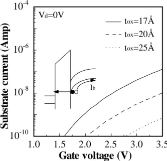
Fig. 4.4a Id degradation versus stress gate bias in nMOSFET's with tox=17Å , 20Å , 25Å and 33Å . Stress Vds is 3.0V for the tox=33Å device and 2.5V for other devices.
Fig. 4.4b Substrate current versus gate bias with Vds=0V. This substrate current results from valance-band electron tunneling.
Fig. 4.5 Illustration of valance-band tunneling enhanced hot electron process.
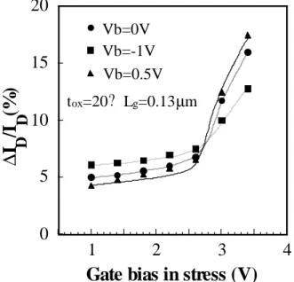
Fig. 4.6a Drain current degradation with different substrate biases in stress, Vbs=0.5V, 0V and -1V. tox=20Å and stress Vds=2.5V.
Fig. 4.6b Drain current degradation with different substrate biases in stress, Vbs=0.5V, 0V and -1V. tox=33Å and stress Vds=3.0V.
Fig. 4.7 Dependence of gate current on substrate bias in stress. Lg=0.13µm and tox=25Å .
Fig. 4.8a Simulated lateral field distributions along the channel.Vds=2.5V, Vgs=3.4V,
Vbs=0V and -1V. The source junction is at x=0.0µm.
Fig. 4.8b Simulated conduction band-edge diagram and electron concentration distribution in the vertical direction from coupled 1D Poisson equation and Schrodinger equation. The centroid of the electron distribution is closer to the Si surface at Vbs=-1V.
Fig. 4.9 Substrate bias dependence of the drain current degradation at two different stress Vgs, 1.3V and 3.4V. The degradation in a stress condition of Vds=2.5V, Vgs=3.4V and substrate floating is indicated.
Fig. 5.1 The dependence of hot electron gate current on substate bias. The threshold voltage of the device is about 1.5V.
Fig. 5.2 The dependence of hot electron gate current on drain bias. The threshold voltage of the device is about 1.5V.
Fig. 5.3 Hot electron light emission spectrum in a nMOSFET with different substrate biases. IL is the light intensity.
Fig. 5.4 Temperature dependence of hot electron gate current at Vbs=0V (CHE) and 1.5V (AECHE). The drain bias is 3.5V.
Fig. 5.5 Max. programming efficiency in a range of 0V=Vgs=7V versus drain bias. Is' is defined as Id+Ib(Vbs/Vds).
Fig. 5.6 Programming characteristics of the CHE and the AECHE at T=25C and 125C. Vds=3.5V.
Fig. 7.1 (a) N-1s spectra and (b) Si-2p spectra of plasma nitrided films at various stages of processing: () after oxidation of Si(100) in NO at 780 ºC, (----) after exposure to N2 plasma, (⋅⋅⋅⋅⋅) after 30 s anneal in N2 at 950 ºC, (⋅-⋅-⋅) after 60 s anneal in N2O at 950 ºC.
Fig. 7.2 (a) N1s spectrum and (b) Si2p spectrum with background removed for plasma-nitrided film after 15 s anneal in N2O at 950ºC: (•••) measured, (----) fit peaks, () sum of fit peaks, (⋅⋅⋅⋅⋅) residual errors.
Fig. 7.3 XPS spectra of thick silicon dioxide (----) and silicon nitride films () showing the Si 2p features and associated peaks caused by inelastic scattering. Fig. 7.4 Thickness and oxygen/nitrogen concentrations ratio as a function of annealing
time in N2O at 950 ºC for silicon oxynitride films deposited by LPCVD on Si(100): (●●●) thickness from XPS, (▲▲▲) equivalent oxide thickness determined from XPS measurements and calculated dielectric constant, (○○ ○) [O]/[N] from XPS measurements, (□) XPS thickness for Si (100) oxidized in N2O at 950 ºC.
Fig. 7.5 Thickness and oxygen/nitrogen concentrations ratio as a function of annealing time in N2O at 950 ºC for silicon oxynitride films formed by oxidation of Si(100) in NO followed by plasma nitridation: (●●●) thickness from XPS,
oxide thickness determined by electrical measurements, (▲▲▲) equivalent oxide thickness determined from XPS measurements, (○○○) [O]/[N] from XPS measurements.
Fig. 7.6 The number of silicon bonds (magnitude of 4/(2x + 3y)) calculated using the XPS measurements for the plasma-nitrided (●●●) and LPCVD (■■■) films as a function of annealing time in N2O at 950 ºC.
Fig. 7.7 Capacitance per unit area at 100 kHz vs voltage for plasma nitride film annealed for 30 s in N2O at 950 ºC: (●●●) measured, () fit from NCSU CV program [52].
Fig. 7.8 Current density vs voltage for plasma nitride film annealed for 30 s in N2O at 950 ºC: () measured, (⋅⋅⋅⋅⋅) calculated from expression of Brar et al. [58]. Fig. 7.9 Calculated XPS thickness, d, divided by equivalent oxide thickness, deq, for
films consisting of a layer of silicon dioxide on top of a layer of silicon nitride (open symbols) or a layer of silicon nitride on silicon dioxide (solid symbols): (●●●) deq = 2.0 nm, (■■■) deq = 1.5 nm, (▲▲▲) deq = 1.0 nm.
Table Captions
Table1:
Full width at half maximum (FWHM) and binding energy (BE) of the N-1s XPS peak for plasma-deposited silicon oxynitride films after various process steps during formation and after annealing at 950 ºC in N2O.
Chapter 1 Intr oduction
The supply voltage for ULSI circuits will have to be reduced as channel length decreases due to hot electron reliability limitations. In contradiction to predictions based on the simple lucky carrier concept [1], non-negligible hot carrier degradation has been observed in MOS devices even at a drain bias below the threshold for interface state generation (Φit ~ 3.7eV) [2-6]. There are several possible mechanisms for low-voltage hot carrier degradation. For example, by using Monte Carlo or other simulation techniques to nMOSFET's, it has been predicted that at the drain voltage below 3V, electrons heated by electron-electron (e-e) scattering should dominate the high-energy tail of the electron energy distribution function above Φit [7,8]. Moreover, Monte Carlo simulations and theoretical considerations suggest that the electron-phonon interaction at high energies in the silicon conduction band can lead to a quantum-mechanical collisional broadening which results in a dispersion of the electron energy levels [9]. Recently, Auger recombination has also been proposed to be a major mechanism for supplying the additional required energy for hot electron degradation at a low applied voltage [10], [11]. This process involves electron and hole recombination, transferring their energy to another electron. Thus, the high-energy tail of channel electrons is increased.
Recently, the feasibility of applying a positive substrate bias in nMOSFET's to achieve better performance has received extensive attention in certain analog and digital circuits. For example, enhanced low-power analog performance can be achieved by applying a positive substrate bias that enables reduced short channel effects [12]. Less threshold voltage roll off suggests that a better device matching property can be obtained. Hsu et al. demonstrated that buried-channel (B.C.) MOSFET's operated in DTMOS-like operation mode (Vgs=Vbs) is more appropriate for low-noise analog applications [13]. In addition, a DTMOS that is suitable for low voltage ULSI circuits was proposed [14,15]. The on-state threshold voltage in this structure is reduced by forward biasing the substrate,
resulting in a significantly higher Ion/Ioff ratio than the conventional MOSFET's as shown in Fig.1.1. The applied substrate bias here is sometimes as large as 0.7V [16] or even larger [17,18]. However, the reliability issue of MOSFET's in such a bias condition has seldom been studied. In this work, we report a new hot carrier degradation mode in DTMOS operation. The observed degradation cannot be simply explained by conventional channel hot electron theory. Instead, an Auger recombination assisted hot electron energy gain process is proposed. The hot electron gate injection current and light emission spectrum, which reflects the high-energy tail of the channel electrons have been measured to support our model. The temperature and the substrate bias dependencies of the Auger effect in DTMOS operation are characterized. The Auger enhanced degradation exhibits positive temperature dependence and may become a serious reliability problem at a high temperature. Besides, enhanced hot carrier degradation with stress Vg in the valence-band tunneling regime is observed in ultra-thin gate oxide MOSFET's. This degradation is attributed to channel hole creation by valence-band electron tunneling. The created holes provide for Auger recombination with electrons in the channel and thus increase hot electron energy. In ultra-thin gate oxide nMOSFETs, our result shows that the valence-band tunneling enhanced degradation, as opposed to maximum Ib stress induced degradation, exhibits positive dependence on substrate bias. This phenomenon may cause a severe reliability issue in floating substrate or positively biased substrate devices. On the other hand, by taking advantage of the Auger recombination assisted hot electron energy gain process, a new HE programming technique is proposed for flash EEPROM operation. The proposed method provides a faster programming rate and higher electron injection efficiency than the conventional hot electron programming. This technique also shows excellent temperature stability from T=25C to T=125C. This method is promising in low voltage and high temperature operation.
Except the hot carrier reliability issues, intrinsic gate leakage current is also an incoming problem. Silicon nitride and oxynitrides are being evaluated as replacements for silicon dioxide in the gates of aggressively scaled CMOS devices. Although boron penetration and hot-electron stress effects can potentially be reduced by mono-layer quantities of nitrogen, larger nitrogen concentrations result in a higher dielectric constant, allowing for reduction of the direct tunneling currents. Treatment of the Si (100) surface with a nitrogen plasma results in the formation of a defective silicon nitride layer. In order to reduce defects in gate-quality oxynitrides, they are often annealed in nitrous oxide [19] after formation, and this results in an increase in the oxygen content of the films. Previous work has focused on measuring the redistribution of nitrogen at the interface between Si (100) and silicon dioxide films during N2O annealing [20], or the effect of long (up to 30 min) oxidations of silicon nitride films in N2O [21]. The amount of nitrogen left in ultra-thin oxynitride films after rapid thermal oxidation in N2O has not been the subject of much comment by those who measure equivalent oxide thickness using capacitance measurements.
A major reason for this is the difficulty of determining the nitrogen profile of ultra-thin films since ion-beam techniques such as medium-energy ion scattering [20], or narrow resonance nuclear reaction analysis [22] are not readily available for routine analysis, while other methods such as secondary-ion mass-spectrometry [23] have reached their resolution limits. A simple and generally available technique such as X-ray photoelectron spectroscopy (XPS) can give useful information such as the film thickness and the oxygen/nitrogen concentration ratio and can provide a measure of the non-uniformity with depth.
A recent review discusses much of the literature describing the XPS analysis of ultra-thin silicon dioxide films [24]. It highlights the sensitivity of ellipsometry measurements to surface contamination, in contrast to the XPS technique that involves a ratio of two peak areas equally attenuated by contaminants. XPS measurements on SiO2
films have also been carefully calibrated against other techniques such as transmission electron microscopy and capacitance-voltage (CV) measurements [25]. Previous work was facilitated by the relative simplicity of growing a number of stoichiometric silicon dioxide films with thickness in the range of interest. For silicon nitride films the calibration is more difficult since it cannot generally be assumed that nitrogen concentration does not change with film thickness.
In this paper the equivalent oxide thickness of plasma-nitrided films annealed in N2O at 950 ºC was determined by capacitance-voltage (CV) measurements, and the quality of these films was determined by CV and current-voltage (IV) measurements. The thickness of N2O-annealed oxynitride films produced by plasma nitridation and by low-pressure chemical-vapour deposition (LPCVD) was determined by analysis of the Si-2p (substrate) and Si-2p (bonded) XPS lines and their composition was determined by analysis of the N-1s and O-N-1s lines. The electron escape depth of Si-2p electrons from silicon nitride was determined by comparing the yields in thick silicon nitride and silicon dioxide standards. The XPS measurements, coupled with interpolations from the silicon dioxide and silicon nitride standards, were used to self-consistently recalculate the thickness. The dielectric constant determined from a Bruggeman effective medium approximation [26] using the oxygen/nitrogen ratio was then used to calculate the equivalent oxide thickness for comparison with the CV measurements. Finally, estimates are made of potential errors in the XPS analysis introduced by assuming that the films have uniform composition with depth.
In this study, Chapter 2 contains a brief description of device characterization and Auger recombination assisted hot electron energy gain process. The measured hot electron gate current and the photon luminescence spectrum are also shown in this Chapter. These measurements confirm that the increase of the high-energy tail of channel electrons results from the DTMOS operation mode. In addition, the device simulation
evidence that Auger effect is significantly enhanced under such a bias condition. In Chapter 3, Auger recombination enhanced device degradation in DTMOS operation mode is measured. The temperature and bias effects on the Auger enhanced degradation are also analyzed. In Chapter 4, valence-band tunneling enhanced hot carrier degradation in ultra-thin oxide nMOSFET’s is observed. This phenomenon is also attributed to Auger recombination effect. The substrate bias dependence of valence-band tunneling enhanced hot carrier degradation is examined. Moreover, we demonstrate a new hot electron programming technique by taking advantage of Auger recombination enhanced gate injection current in flash EEPROM in Chapter 5. Improved hot electron injection efficiency and temperature stability can been obtained. The fabrication process flow and characterization method for advanced gate dielectrics will be described in Chapter 6. In Chapter 7, the characteristics of fabricated ultra-thin gate dielectrics will be shown. The thickness of the dielectrics has been verified by C-V method and XPS analysis. Furthermore, the bonding configurations are also analyzed by XPS method. The conclusions drawn from this work were embodied in Chapter 8.
Chapter 2 Evidence of Auger Recombination Assisted Hot Electr on
Ener gy Gain Pr ocess
2.1 Device Char acter ization Method
A four-terminal nMOSFET was used with a gate width of 100µm and a gate length of 0.25µm. The device has a gate oxide thickness about 50Å . Maximum Ib stress around Vg=0.5Vd was performed in DTMOS-like mode (Vb>0) and in the standard mode (Vb=0). Drain current in the triode region was measured to monitor drain current degradation. Temperature and drain bias dependence of the Auger enhanced degradation was also characterized. Hot carrier luminescence measurement was performed with single photon counting system that allowed for spectral analysis in the range 1.2eV-2.9eV [27]. Photons emitted from a MOSFET are detected by a photon counting camera through the optical microscope. The photon numbers at each wavelength are counted individually using band pass filters. The measured data are then corrected for the energy dependence of the filter transmittance. During the luminescence measurement, drain current was monitored to check the possible presence of aging, which was found to be negligible.
2.2 Auger Recombination Assisted Hot Electr on Ener gy Gain Pr ocess
It has been reported that Auger recombination can enhance hot electron tail and cause more serious degradation in MOSFETs [11], [28], [29]. The process for Auger recombination in various device operation conditions is illustrated in Fig.2.1. In Fig.2.1 (a), a small part of holes created by impact ionization may flow to the region near the source (where electron concentration is high) [30] and provide for Auger recombination. In Fig.2.1 (b), a positive substrate bias is applied and the channel hole concentration and thus Auger recombination rate are increased due to substrate hole injection [29]. In ultra-thin oxide nMOSFETs, a positive gate bias can cause valence-band electron tunneling to
the gate and leave holes behind in the channel (Fig.2.1 (c)). In the following, we will first investigate the significance of positive substrate bias injected holes to device reliability.
Fig.2.2 illustrates the electron energy gain process in conventional hot carrier stress and in DTMOS hot carrier stress, respectively. In conventional hot carrier stress, the electron energy gain mechanism is field heating near the drain junction as shown in Fig.2.2 (a). In DTMOS hot carrier stress, i.e., with a positive substrate bias applied, holes are injected from the positively biased substrate to the channel as shown in Fig.2.2 (b). The injected holes can provide for recombination with electrons in the channel and give excess energy to other channel electrons as shown in Fig.2.3 (a). This is the Auger recombination process and also a major energy gain process in DTMOS operation. The energetic electrons arising from the Auger process are then accelerated by a channel electric field, thus resulting in a larger hot electron tail than in the standard MOSFET’s operation condition as shown in Fig.2.3 (b).
2.3 Hot Electr on Light Emission Measur ement
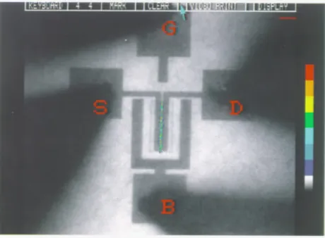
As we know, the hot electron luminescence and the light emission in nMOSFET's can reflect the electron energy distribution [31], [32]. Fig.2.4 (a) and Fig.2.4 (b) are the micrographs of the hot electron light emission from nMOSFET's with Lg=0.25µm and
Wg=100µm. Bias conditions are: Vds=2.9V, Vgs=1.5V, Vbs=0V and Vds=2.9V,
Vgs=1.5V, Vbs=0.7V, respectively. The bandwidth of the band pass filter is 800Å . Square block regions are aluminum pad with 100µm by 100µm for electrical contacts. The total exposure time is 100 seconds. Note that the light intensity is relatively stronger as the positive substrate bias is applied. Fig.2.5 shows the light intensity and the substrate current as a function of the gate voltage with different substrate biases. It should be mentioned that the substrate current arising from impact ionization near the drain junction strongly depends on channel field and so does the hot electron light emission. Therefore, the hot electron light emission correlates well to the substrate current in the conventional
hot carrier stress. However, the substrate current in the DTMOS hot carrier stress condition is more complex due to an additional current path from the substrate to the channel. Therefore, the light emission provides a reliable monitor for hot electron energy in MOSFET's, which can be used as an alternative monitor to the substrate current.
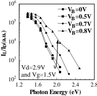
The hot electron light emission spectrum is measured to analyze the hot electron distribution, as illustrated in Fig.2.6 In this figure, the y-axis represents the normalized light intensity and the x-axis represents the photon energy. The light intensity is normalized to the drain current to compensate for the different carrier flux in the channel. As the substrate bias increases from 0V to 0.5V, the hot electron actually decreases due to a smaller electric field. As the substrate bias continues to increase to 0.8V, the hot electron tail is significantly enhanced by an order of magnitude.
2.4 Hot Electr on Gate Cur r ent
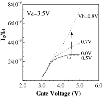
Another evidence is the hot electron gate injection current. Since hot electron gate inction current, Ig, is a sensitive measure of the high-energy tail of the hot carrier distribution [33]. Fig.2.7 demonstrates the normalized hot electron gate injection current as a function of gate bias with different substrate biases. The drain bias is fixed at 3.5V and the substrate bias is increased from 0V to 0.8V. Again, the gate injection current first decreases and then increases with the substrate bias. In Fig.2.8, we measure the hot electron gate current at different drain biases. From the above two figures, the hot electron gate current depends on both drain bias and substrate bias. The drain bias determines the field heating and the substrate bias determines the Auger effect. The dependence on both the drain bias and the substrate bias confirms that the electron energy gain process in DTMOS operation consists of Auger recombination and field acceleration.
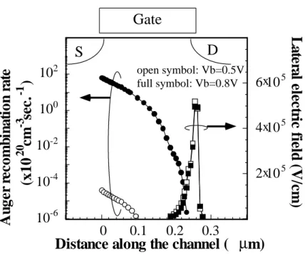
Figure 2.9 shows the two-dimensional device simulation results of the Auger recombination rate and electric field in the channel. In this figure, the x-axis is the distance from the source junction. The open symbol represents the result with a substrate bias of 0.5V and the full symbol represents a substrate bias of 0.8V. Note that the electric field slightly decreases as the substrate voltage increases from 0.5V to 0.8V due to body effect, whereas the Auger recombination rate increases by several orders of magnitude due to the exponential dependence of hole injection. Notably, hole injection is restricted to the low field region near the source. Therefore, the energetic electrons arising from the Auger recombination are then accelerated by a lateral electric field, thus leading to a large hot electron tail, and so do the hot electron light emission and the gate injection current.
Chapter 3 Device Degr adation Enhanced by Auger Recombination
Experimental evidence of the Auger recombination enhanced hot electron tail is shown in the above Chapter. In the following, device performance degradations due to the Auger recombination effect are discussed. The measured result includes on-state drain current degradation, off state drain leakage current degradation and flicker noise degradation.
3.1 On-State Dr ain Cur r ent Degr adation
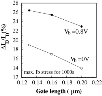
To demonstrate the Auger effect on device reliability, the linear drain current degradation at different substrate biases is measured in the Fig.3.1. Stress drain bias is 2.9V and gate bias is 1.5V. The device has a gate length of 0.25µm. The drain current degradation is increased by an order of magnitude when the substrate bias increases from 0V to 0.8V. The gate length dependence of Auger enhanced degradation is examined in Fig.3.2. The enhanced degradation is still remarkable as the gate length is down to 0.13µm.
3.2 Off-State Dr ain Leakage Cur r ent Degr adation
Figure 3.3 shows the off-state drain leakage current degradation by the conventional hot carrier stress and by the DTMOS hot carrier stress. The dashed line represents the conventional hot carrier stress and the dotted line is the DTMOS hot carrier stress. At a medium drain bias, the drain leakage current degradation is primarily caused by interface trap creation. Fig.3.4 shows the drain leakage current enhancement by the two stresses. Apparently, the drain leakage degradation by the DTMOS hot carrier stress
Vds=0.1V versus the off-state drain leakage current (Ioff) measured at Vgs=0V and Vds=1.5V with different stress substrate biases. Note that the Ion/Ioff characteristics in
the Lg=0.13µm device after DTMOS hot carrier stress is worse than that of the Lg=0.2µm
device. This means that short gate length nMOSFET's operated in the DTMOS operation mode has a severe reliability problem.
3.3 Flicker Noise Degr adation
With respect to analog devices, we compare the flicker noise degradation by the conventional hot carrier stress and by the DTMOS hot carrier stress. As shown in Fig.3.6, the flicker noise degradation by the DTMOS hot carrier stress is enhanced by several times. Therefore, analog devices in DTMOS operation will suffer from a higher drain current noise.
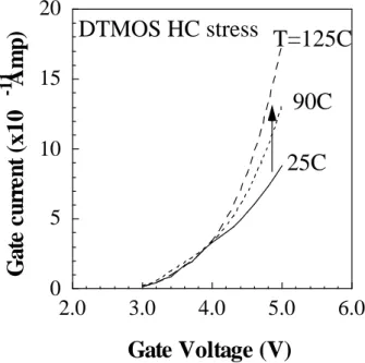
3.4 Temper atur e Dependence
Historically, elevated temperatures resulted in a decrease in hot electron gate current (and hot carrier damage) due to increased phonon scattering [34], [35]. Fig.3.7 compares the temperature dependence of hot electron gate injection current in the conventional hot carrier stress and in the DTMOS hot carrier stress. The gate injection current in the conventional hot carrier stress has negative temperature dependence. However, the gate current in the DTMOS hot carrier stress exhibits positive temperature dependence. The reason for the positive temperature dependence is two-fold; first, the substrate hole injection increases with the temperature. Second, the Auger recombination rate itself has a positive temperature coefficient [36]. To our knowledge, a positive temperature dependence of hot electron gate injection current is observed here for the first time.
Figure 3.8 illustrates the temperature effect on the drain current degradation by the two stresses. As the temperature is increased from room temperature to 125C, the degradation by the DTMOS hot carrier stress is enhanced by about ten times. This point is particularly important to device reliability since today's high performance devices are required to operate in such high temperature range.
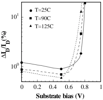
3.5 Substr ate Bias Effect on Auger Enhanced Degr adation
The substrate bias effect on the Auger enhanced degradation is investigated in Fig.3.9. The corresponding stress drain current is shown in Fig.3.10. As shown in Fig.3.9, the drain current degradation shows opposite temperature dependence in the low substrate bias region and in the high substrate bias region. In the low substrate bias region, the field heating is the dominant electron energy gain process. Therefore, the drain current degradation reduces at a higher temperature because of a larger phonon scattering rate. In the high substrate bias region, both the Auger effect and field heating play a major role in the electron energy gain process and, as mentioned previously, the former mechanism has a positive temperature effect. Furthermore, this figure also shows that the critical substrate voltage for the onset of the Auger enhanced degradation decreases as the temperature increases. The threshold substrate bias for the onset of the Auger effect is about 0.5V at 125C.
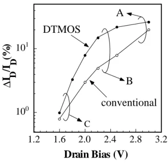
3.6 Dr ain Bias Dependence of Auger Enhanced Degr adation
Figure 3.11 demonstrates the dependence of Auger enhanced drain current degradation on the stress drain bias. At a relatively high drain bias (region A), the field heating itself is sufficient to cause severe degradation. Thus, the degradation by
drain bias reduces (region B), electrons by field heating solely do not gain sufficient energy for interface trap creation. As a result, the combination of Auger recombination and field heating processes can increase the hot electron energy above the threshold for trap creation. Consequently, the Auger enhanced degradation appears to be more significant. Finally, at an extremely low drain bias (region C), the Boltzmann distribution tail is believed to be dominant and the degradation is almost independent of the substrate bias.
Chapter 4 Valence-Band Tunneling Enhanced Hot Car r ier Degr adation
in Ultr a-Thin Oxide nMOSFET’s
It has been shown in literature that in short gate-length devices hot carrier degradation at Vgs˜Vds stress is more serious than at maximum Ib stress (Vgs~0.5Vds) [37], [38]. Fig.4.1 (a) and 5.1 (b) shows the drain current degradation in two different gate-length nMOSFETs, Lg=0.20µm and Lg=0.13µm, respectively. The gate oxide thickness is tox=25Å . The corresponding Ib in stress is plotted in Fig.4.2. In the 0.13µm device, the degradation increases first slightly with stress Vgs. This characteristic was explained in [38] because the channel hot electrons are confined more closely to the Si surface at a larger Vgs. As stress Vgs increases above 3V, a drastic rise of the degradation is noticed in both devices. Further study reveals that the degradations at a low stress Vgs and at a high stress Vgs are both due to interface trap creation (Fig.4.3).
To investigate the correlation of the rise of the degradation with valence band tunneling, we measured Id degradation and valence-band tunneling current in nMOSFET's with different tox (Fig.4.4). The tox=33Å device has a gate length of 0.16µm and other devices have a gate length of 0.13µm. The substrate current measured at Vds=0V, which reflecting valence-band tunneling, is shown in Fig.4.4 (b). The following features should be noted. First, the rise of the Id degradation in the valence-band tunneling regime is observed in all the devices except for the tox=33Å device. The valence-band tunneling current in the 33Å device is found to be negligible (result not shown in Fig.4.4 (b)). Secondly, the degradation at maximum Ib stress decreases when tox reduces. This part is in agreement with the conclusion by Momose [39]. However, an opposite trend (i.e., the degradation increases as tox reduces) is found when the devices are stressed in the valence-band tunneling regime. The process for valence-band tunneling enhanced hot carrier stress is proposed in Fig.4.5. In Fig.4.5 (a), channel holes are created
recombination with electrons in the channel and transfer the excess energy to other conduction electrons (Fig.4.5 (b)). The energetic electrons arising from the Auger process are subsequently accelerated by a lateral electric field (Fig.4.5 (c)), thus resulting in a larger interface trap generation rate. The entire electron energy gain process therefore depends on Vgs (valence band tunneling) and Vds (lateral field acceleration)
To further verify the role of valence-band tunneling created holes in the degradation, we change the substrate bias in stress (Fig.4.6). Fig.4.7 shows the dependence of gate current on substrate bias in stress. For tox=20Å devices (Fig.4.6 (a)), the degradation in the low Vgs region and in the high Vgs region exhibits opposite substrate bias dependence. The simulated lateral electric field distribution and the conduction band-edge diagram in the vertical direction are plotted in Fig.4.8. As Vbs changes from 0V to -1V, the peak lateral channel field slightly increases, implying stronger lateral field heating. Moreover, the vertical field is also increased, which means the channel electrons are pushed further toward the Si surface. These two factors lead to a larger gate current (Fig.4.7) and increased Id degradation in the low Vgs region. In the high Vgs region, we have shown valence-band tunneling plays a role in the degradation. A negative substrate bias can help remove the channel holes to the substrate and thus reduce the hole effect. As a result, the Id degradation becomes smaller at a negative substrate bias although the stress gate current is larger (Fig.4.7). This result actually excludes the possibility that the rise of the Id degradation at a large Vgs is primarily caused by the increase of stress Ig.
In contrast, the tox=33Å device shows negative substrate bias dependence in the entire range of stress Vgs because of negligible valence-band tunneling effect. In Fig.4.9, we plot the Id degradation versus the substrate bias in stress. The stress gate bias is 1.3V for the lower curve and 3.4V for the upper curve. The degradation in a floating substrate stress condition is also indicated in the figure.
Chapter 5 Auger Recombination Enhanced Hot Electr on Pr ogr amming
in EEPROMs
A stack-gate EEPROM cell and a conventional gate dummy cell are used in this study. The tunnel oxide thickness is 100Å and the gate length is 0.7µm. The dummy cell has a gate width of 20µm.
5.1 Dummy Cell Char acter istics
Figure 5.1 displays the dependence of hot electron gate current on substrate bias in a conventional gate nMOSFET. The drain voltage is 3.5V. When Vbs increases, the gate current initially decreases due to the reduction of channel lateral field and then increases with Vbs. The Vgs characteristic at Vbs=1.5V differs from that at Vbs=0V. The Igs-Vgs has a peak at Vbs=0V, while the gate current monotonically increases with Igs-Vgs at Vbs=1.5V. Fig.5.2 illustrates the drain bias dependence of hot electron gate injection current. The dependence on both drain bias and substrate bias confirms that the electron energy gain process in this method consists of Auger recombination and field acceleration. Hot electron luminescence and emission spectra are measured to analyze the hot electron distribution (Fig.5.3). The light intensity is normalized to the drain current. This finding confirms that applying a positive substrate bias can increase the high-energy tail of the channel electrons. In addition, Fig.6.3 shows a small hump around 1.6eV (=1.5Eg) with a positive substrate bias. Theoretically, the most probable electron energy gain in Auger process is about 1.5Eg [40,41]. The appearance of the hump is possibly related to the Auger effect.
The temperature dependence of conventional CHE and AECHE programming is examined in Fig.5.4. The CHE gate current has negative temperature dependence, while the AECHE gate current exhibits slightly positive temperature dependence. This feature
of the AECHE is particularly useful in applications that require high temperature operation.
The injection efficiency (Ig/Is') of AECHE is evaluated in Fig.5.5, where Is' is defined as Id+Ib(Vbs/Vds) to account for the voltage difference at the substrate and at the drain. Notably, although a large lateral BJT current exists in the AECHE operation, the programming efficiency of the AECHE is still much better than the CHE. In addition, diminishing temperature instability in programming efficiency is obtained in the AECHE.
5.2 EEPROM Char acter istics
Figure 5.6 presents the programming characteristics in a EEPROM cell by the CHE and AECHE. Vcg is 12V and Vbs is 1.5V in the AECHE and Vcg is 6V in the CHE. The drain bias is 3.5V. To our knowledge, positive temperature dependence of the HE programming speed is reported for the first time in the AECHE. In contrast to the CHE, a 5x programming speed enhancement factor in the AECHE is obtained at T=25C. The speed enhancement factor is even larger at 125C. Besides, the fact that a higher Vcg is allowable in the AECHE makes it possible to achieve a larger threshold voltage window between the programmed state and the erased state.
Chapter 6 Fabr ication Pr ocess and Char acter ization Technique of
Advanced Gate Dielectr ics
6.1 For mation of Oxynitr ides
Si (100) wafers (0.025 ohm-cm n-type) were given a HF-last RCA clean prior to film deposition. Two types of silicon oxynitride were studied in this work. One set was formed by first oxidizing the wafers in nitric oxide (NO) at a pressure of 4 mTorr for 6 minutes at 780 oC. Without breaking vacuum, these wafers were exposed to nitrogen plasma for 5 s at a substrate temperature of 300 oC. The plasma was formed using 450 Watts of absorbed microwave power and 15 sccm of molecular nitrogen in an electron-cyclotron resonance (ECR) apparatus (described previously [42]) positioned 50 cm from the silicon substrates.
Another set of films, produced for comparison purposes, was formed by a standard low-pressure chemical-vapor deposition with silane and dichlorosilane at 780 oC. These were given a rapid anneal in flowing nitrogen for 30 s at 1000 oC to densify the films prior to oxidation.
6.2 Oxidation of Oxynitr ides
The wafers were introduced into a Heatpulse 610 (Steag RTP Systems) rapid thermal processor (RTP) where they were first heated in flowing nitrogen for 4 minutes at 500 oC to drive off water vapor. The plasma nitrided wafers were immediately given a 30 s anneal in N2 at 950 ºC to densify them prior to the oxidation in N2O but this step was omitted for the LPCVD wafers since they were annealed in N2 immediately after the LPCVD deposition. All the films were oxidized in flowing N2O at 950 ºC. To compensate for the optical absorption by N2O [43], the RTP pyrometer was calibrated by performing measurements on a test wafer with an embedded thermocouple. The accuracy
6.3 XPS Analysis of Oxynitr ides
The analysis of film composition was done using a PHI XPS instrument which employed a non-monochromatic MgKαX-ray source with a hemispherical electron energy analyser at an angle θ = 45º from the wafer normal (standard x-ray source position 54.7 º from analyser). Spectra were obtained with a band-pass energy of 23.5 eV, resulting in an energy resolution of ~1 eV.
A technique for background removal, correcting the measured spectra for inelastic scattering, has been formulated by Tougaard [44] in terms of an inelastic scattering cross-section that varies with the energy lost as a result of the inelastic scattering. Calculations using the inelastic scattering cross-sections for SiO2 provided in Ref. [44] have been used to evaluate the effect of inelastic scattering. The resultant primary excitation spectra were not significantly different than the spectra obtained from the measured peaks using a linear background correction. This was expected since the inelastic scattering must be small for scattering events that result in energy losses less than the oxynitride band-gap (> 5eV). The analysis of Tougaard [44] has shown that the commonly used Shirley background correction cannot be correct; however, its use would not result in significant changes in the measured intensity ratios, since the background is relatively flat under the main peaks.
The O1s and N1s peak areas were obtained from the fits of one or two Gaussian-Lorenzian functions to the observed spectra. The Si 2p peak was fit with two features: the 2p3/2-2p1/2 doublet characteristic of electron emission from the Si substrate, and a broader Gaussian-Lorenzian peak due to emission from the overlying film. The doublet was characterized using a Si (100) wafer given an RCA-HF last clean and these features (0.61 eV splitting, 2:1 area ratio, 70% Gaussian-30% Lorentzian lineshape) were used for the fitting of the spectra of the oxynitride films. The fit of the oxynitride Si2p spectra thus involved optimizing seven parameters, the full width at half-maximum intensity (FWHM)
of the doublet, its intensity, its position, the intensity of the Si2p (oxynitride) peak, its FWHM, its position, and the ratio of Gaussian/Lorenzian components in its line shape. In the following the subscripts o, n, on, and Si are used to designate parameters for the O1s, N1s, Si2p (substrate), and Si2p (bonded to O and N) features, respectively. It is assumed that the films are homogeneous, and this assumption will be investigated in more detail later. Thus λo, λn, and λon are the electron escape depths for the O1s, N1s,
and Si2p electrons in an oxynitride film, So, Sn, and Son are the atomic sensitivity factors,
and Co, Cn, and Con are the concentrations of oxygen, nitrogen and silicon atoms in the
film. The parameter λSi is the electron escape depth for Si2p electrons in the silicon
substrate, Csi is the concentration of silicon atoms in the substrate, and d is the film
thickness. The following quantities involving the areas, Io, In, Ion, and ISi, of the four
features were used in the analysis of the films [45, 46]:
], 1 / ln[ ) cos( + = on Ion onISi d λ θ β (1) , )] cos / exp( 1 [ )] cos / exp( 1 [ θ λ θ λ o o n n n o n o d S I d S I C C R − − − − = = (2) , )] cos / exp( 1 [ )] cos / exp( 1 [ θ λ θ λ o o on on on o on o d S I d S I C C − − − − = (3) and , )] cos / exp( 1 [ )] cos / exp( 1 [ θ λ θ λ n n on on on n on n d S I d S I C C − − − − = (4)
where βon = λonCon/λSiCsi. The sensitivity factor ratios in Eqs. (1)-(3) are related to the
escape depths [45] by So/Son = Toλo/Tonλon and Sn/Son = Tnλn/Tonλon, where To, Tn, and Ton
are the transmission of the electron analyzer at the energies of the O1s, N1s, and Si2p electrons, respectively. The escape depths were calculated for the O1s and N1s electrons from those for the Si2p electrons using the following expressions:
m on
o λ (720/1150)
where the O1s, N1s and Si2p electrons have energies of 720, 855, and 1150 eV, respectively. A value of m = 0.5 has been used by Seah and Dench [47] and a value of m = 0.7 gives a good fit to the data of Tanuma et al. [48]. In fact, choosing any value between m = 0.5 and m = 0.7 results in negligible changes in the calculated values of d, and changes in R of <1.5%. With the use of Eq. (5), the sensitivity factor ratios become independent of oxynitride film composition, as is often assumed.
To calibrate the XPS thickness measurements, spectra were obtained from thick SiO2 and silicon nitride films. The former was a thermal oxide grown at 1050 oC in O2, while the latter was a high-quality silicon nitride film deposited using a plasma-CVD process [42] which results in a [N]/[Si] ratio of 1.37, as determined by nuclear reaction analysis (NRA) and Rutherford backscattering (RBS) measurements of the nitrogen and silicon contents, respectively. This sample is slightly nitrogen rich, consistent with the <5% at. % hydrogen bonded as NH [42]. The density of silicon dioxide was taken as 2.27 g/cm3 [49] corresponding to a density of silicon atoms Cox = 2.28×10²² at./cm3 . The
density of the silicon nitride film was determined from the NRA and RBS measurements and the thickness obtained by ellipsometry [42, 50]. This gave a value for the density of 2.95 g/cm3 which corresponds to a silicon concentration Cnit = 3.80×10²² at./cm3. The
nitride wafer was given a 30 s clean in 1% HF solution, rinsed, and blown dry, and the substrates were placed side-by-side on a metal mount along with a piece of Si (100) given an RCA HF-last clean. Spectra were obtained for all three samples, taking care to ensure that the spectrometer alignment and incident x-ray intensity was the same for all three. Since the films of interest had excellent electrical properties after annealing, it was assumed that the oxynitrides, consisting of molecules of SiOxNy, were free of O-N, Si-Si
and dangling bonds; i.e., that x/2+ 3y/4= 1, (“Mott’s law” [51]). It follows that x is related to the oxygen/nitrogen concentration ratio, R, by x = 4R/(3+ 2R). In Appendix A it is shown that the escape depth in an oxynitride film can be given to a good approximation
by a linear interpolation between those for pure silicon dioxide and nitride films, λox and
λnit, respectively, viz:
. ) 2 3 ( 3 2 2 ) 2 ( R R x x ox nit ox nit on + + = − + = λ λ λ λ λ (6)
Finally, it will be shown that βon differs by <5% for silicon nitride and silicon
dioxide so only a small error will be introduced by using the following linear interpolation between the values for pure silicon dioxide and nitride films, βox and βnit,
respectively: . 2 ) 2 ( nit ox on x xβ β β = + − (7)
Since the electron escape depths depend on the oxygen/nitrogen ratio, and the determination of the latter depends on the calculated thickness, we have used a simple iterative procedure to calculate x and d. It uses pure silicon dioxide values as the initial guesses for λon and βon . The iterations, which can be carried out on a simple spreadsheet,
involve calculating Eqs. (1), (2), (5), (6) and (7) and then repeating the sequence starting at Eq. (1). Convergence to <0.1% can be obtained after 2 or 3 iterations.
6.4 Electr ical Measur ements
Al-gated capacitors were made by evaporating aluminum through a shadow mask followed by annealing in forming gas at 380 ºC for 20 minutes and back contacts were made with In-Ga eutectic. The area of the capacitors, ~5×10⁻⁴ cm2, was measured to an accuracy of ±2% with a calibrated digitizing camera. Electrical measurements were made by probing the Al gates in a probe-station attached to two instruments, a multi-frequency
4140B). High frequency CV measurements were made by stepping with 0.1 V steps each second, first from –3 V to +3 V and then in the reverse direction to look for hysteresis. IV characteristics were obtained with the picoammeter by stepping the voltage source from 0 volts in a positive direction (towards accumulation) until breakdown, which was characterized by a steep rise to currents above 10-2 A. The equivalent oxide thickness was obtained from the 100 kHz CV characteristics by using the NCSU CV fitting routine [52] which includes quantum effects in the channel.
A. Hajii et al. [26] have used a Bruggeman effective medium approximation to estimate the dielectric constant, κoxnit, of oxynitride films in terms of the value of x:
. 89 . 0 82 . 4 85 . 8 2 x x oxnit = − + κ (8)
The coefficients were determined for oxynitride films produced by LPCVD with low oxygen contents but the estimate has been used here for our films with higher values of x. The equivalent oxide thickness, deq, was calculated from the XPS thickness using the
Chapter 7 Analysis of Advanced Gate Dielectr ics
7.1 Char acter istics of the N-1s XPS Peak
The N1s spectra for some of the plasma-nitrided samples are shown in Fig. (1a) and the fit of a single peak to a spectrum is shown in Fig. (2a) for the sample given a 15 s anneal in N2O. The deviation between the measured spectrum (solid circles) and the fit peak (solid line) is shown by the dotted line (residual errors). With one exception, all the N1s spectra were well fit by one peak. The N2 plasma increases the FWHM of the N1s spectrum from 1.46 to 1.73 eV and for this spectrum a better fit is produced using two peaks, one at 398.3 eV with 31 % of the total area, and the other at 398.8 eV. Subsequent annealing reduces the FWHM to 1.57 eV, as shown in Table I. The peaks were referenced to the Si2p3/2substrate peak at 99.9 eV, so sample charging or bandbending in the Si substrate could contribute to the small shifts from 398.3 to 398.8 eV shown in Table I. The high-resolution XPS measurements of Hussey et al. [53] identified two components in this energy range, a 398 eV peak assigned to Si3N4, and a 398.8 eV assigned to an oxynitride species of the form N-Si-O. Others have ascribed a peak at 398.6 eV to bonding states where each N atom is bonded to only two Si atoms, leaving a nitrogen dangling bond [54]. No feature near 400.7 eV attributable to N-O bond [55] was observed in any of the plasma-nitrided films after annealing in N2O.
The N1s peak was at 398.5 eV for all the LPCVD samples, the FWHM was 1.70 eV before N2O oxidation, and the FWHM was 1.66 ± 0.01 eV for all the oxidized LPCVD samples. The main peak was fitted with one component and there was no peak near 400.7 eV attributable to N-O bonds. However, the LPCVD films showed a small satellite, which was observable after the N2O oxidation, with < 0.3 % of the area of the main peak situated at 4.2 eV to the high binding energy side of the main peak. This feature has previously been attributed to screening effects associated with the formation
The Si2p spectra for the plasma-nitrided films are shown at various stages of processing in Fig. (1b). The spectral decomposition of the spectrum for the plasma-nitrided film after a 15 sec oxidation in N2O is shown in Fig. (2b) with the background removed. The sum of the residual errors for the fits are typically < 0.3% of the area of the measured peak areas for all the films after annealing in N2 or N2O at 950 ºC. The residuals could be reduced by the addition of more components to the fits but the improvements were not statistically significant. The maximum errors in the area ratio of the Si2p (bonded) to the Si2p (substrate) peaks were estimated to be ~ ±10 %.
7.2 XPS Calibr ation
Analysis of the O1s signal from the silicon nitride sample indicated that there was approximately an amount of oxide on the nitride surface that would be contained in a 0.12 nm layer of silicon dioxide. Since a heater or sputter gun were not available on the XPS system to remove this contamination, which was probably mostly water, the measured peak areas were corrected by assuming there was a 0.12 nm thick fictitious layer on the surface of both the oxide and nitride standards that absorbed like silicon dioxide but contained no silicon. The sensitivity ratio obtained from the nitride standard was Sn/Son =
1.59, and that from the silicon dioxide standard was So/Son = 2.54, resulting in So/Sn =
1.59.
The Si2p spectra for the oxide and nitride standards, shown in Fig. (3), are remarkably similar. The intensities, Iox and Init of the main Si 2p peak near 103 eV were obtained by
integration using a linear background which, as discussed above, is consistent with Tougaard’s background correction technique [44]. This gave Init/Iox = 0.97±0.04. For SiO2, the value of βox = 0.75 and λox = 2.96 nm were taken from Ref. [25], and the values, βnit =
βnit/ βox = Init/Iox = (λnitCnit)/( λoxCox). The calculated Si2p electron escape depth for
silicon nitride is 33% smaller than the value of 2.59 nm obtained from the parameters of Seah and Dench [47].
For comparison with prior studies, the broad feature between 109 and 140 eV in Fig. (3) associated with inelastic scattering was integrated using a Shirley background. The yields, Yox and Ynit, were estimated for the oxide and nitride films, respectively, by
taking the ratios of the main peak intensity to the sum of the intensities of the main and plasmon peaks, Init(∞) or Iox(∞), for the nitride and oxide samples. The results were
Init(∞)/Iox(∞) = 1.03±0.04, Yox = 0.70 and Ynit = 0.68. The value for SiO2 is identical to
that found in Ref. [25]. The yields were not used in our analysis.
7.3 Thickness and Composition of Annealed Films
Figs. (4) and (5) show the calculated thickness (solid circles) and oxygen/nitrogen concentration ratios (open circles) as a function of N2O annealing time for the LPCVD and plasma-nitrided films, respectively. Before oxidation in N2O the silicon oxynitride film formed by plasma-nitridation had an oxygen/nitrogen concentration ratio, R = 1.9. The film deposited by LPCVD initially had more nitrogen but was not pure nitride (with R = 0.9), likely due to water vapour in the LPCVD furnace or the RTP system used for the post-deposition anneal at 1000 ºC. The LPCVD oxynitride films increased in thickness during the first 20 s by only 0.9 nm and the plasma-nitrided films increased by 1.0 nm during the same time. The more rapid oxidation of the plasma-nitrided films even though they initially have more oxygen is probably due to the fact that they are thinner. In Fig. (4) the thickness of a film formed by directly oxidizing a Si(100) wafer given a HF-last RCA clean is shown, for comparison, by the open squares. The oxidations were done for 15 and 30 s at 950 ºC in N2O. The thickness is in agreement with the N2O oxidation measurements of Ting et al. [57], confirming the calibration of our pyrometer.