電子工程學系 電子研究所碩士班
碩 士 論 文
利用矽控整流器當做記憶單元之
系統層級靜電放電暫態偵測電路
On-Chip Transient Detection Circuit
with SCR as Memory Unit
for System-Level ESD Protection
研 究 生: 林宛彥 (Wan-Yen Lin)
指導教授: 柯明道教授 (Prof. Ming-Dou Ker)
利用矽控整流器當做記憶單元之系統層級靜電放電暫態偵測電路
On-Chip Transient Detection Circuit with SCR as
Memory Unit for System-Level ESD Protection
研 究 生:林宛彥
Student: Wan-Yen Lin
指導教授:柯明道教授
Advisor: Prof. Ming-Dou Ker
國立交通大學
電子工程學系
電子研究所
碩士論文
A Thesis
Submitted to Department of Electronics Engineering and Institute of Electronics
College of Electrical and Computer Engineering
National Chiao-Tung University
in Partial Fulfillment of the Requirements
for the Degree of
Master
in
Electronics Engineering
August 2011
Hsin-Chu, Taiwan, Republic of China
~ iii ~
利用矽控整流器當做記憶單元之
系統層級靜電放電暫態偵測電路
學生:林宛彥
指導教授:柯明道教授
國立交通大學 電子工程學系電子研究所碩士班
ABSTRACT (CHINESE)
靜 電 放 電 (Electrostatic Discharge, ESD) 是 造 成 電 子 產 品 遭 受 過 度 電 性 應 力 (Electrical Overstress, EOS) 最主要的原因。近年來,隨著積體電路 (Integrated Circuits, ICs) 技術進步至深次微米製程,同時為了減少電子產品成本,越來越多的積體電路整合 在單一晶片系統上。在先進製程中,較薄的氧化物層和較窄的通道,都會使得積體電路 的產品更容易受到靜電放電的破壞,因此,靜電放電的防護設計在積體電路技術中是一 項很重要可靠度議題。 系統層級靜電放電在近年中的可靠度問題逐漸受到重視。許多電子產品即使已經通 過元件層級靜電放電(Component-Level ESD)規範的測試,仍然無法達到系統層級靜電放 電(System-Level ESD)防護的要求。在系統層級靜電放電防護的測試條件下,快速暫態 雜訊會使得系統進入未知的當機、故障,或是不正常的工作狀態。傳統的解決方法是在 微電子產品之中,加入許多種不同的濾波或是抗雜訊用的分離元件,但卻大幅地增加了 微電子產品的生產成本。因此,對於系統層級靜電放電防護而言,應用於金氧半導體製 程的積體電路設計防護方法可以整合於晶片系統中,減少產品成本,更具有其重要性。
本論文首先利用矽控整流器(Silicon Controlled Rectifier, SCR)元件會被暫態突波觸 發的特性,提出了一種應用於系統層級靜電放電防護的暫態偵測電路設計。電路主要的 原理是利用矽控整流器當作記憶元件。由實驗的結果證實,當有系統層級靜電放電事件 發生時,提出的電路可以成功的偵測並且記憶快速暫態電波在積體電路電源線上產生的
~ iv ~ 干擾現象。 其次,提出一個結合積體電路雜訊濾波器以及暫態偵測電路的四位元暫態對數位轉 換器。利用電流鏡電路,可以放大在電源線之間的等效電容值,在雜訊濾波器上的電容 值可以有效的減小並節省晶片面積,以及避免漏電問題。此轉換器可以成功的將系統層 級靜電放電之電壓轉換為四位元數位碼輸出,因此能夠確切知道積體電路在系統層級靜 電放電測試之下所遭受影響之程度。 這份論文總共分成五個章節。第一章是有關於系統層級靜電放電防護國際法規的內 容和條例;第二章介紹了傳統用來解決系統層級靜電放電防護的方法;第三章為以矽控 整流器做為記憶單元的暫態偵測電路之介紹及實驗結果;第四章提出四位元暫態對數位 轉換器,包括模擬和量測結果;第五章為此份論文的結論和未來展望。
~ v ~
On-Chip Transient Detection Circuit with SCR as
Memory Unit for System-Level ESD Protection
Student:
Wan-Yen
Lin
Advisor:
Prof.
Ming-Dou
Ker
Department of Electronics Engineering and Institute of Electronics
National Chiao-Tung University
ABSTRACT (ENGLISH)
Electrostatic discharge (ESD) is the main reason that causes electrical overstress (EOS) on microelectronic products. Recently, as technology scaling down to the deep sub-micron, more integrated circuits are integrated into single chip to decrease the cost of microelectronic products. Due to thinner oxide and shallower junction depth in advance technology, microelectronic products equipped with CMOS ICs are more susceptible to ESD damage. Therefore, ESD protection has become an important reliability issue in CMOS ICs.
System-level ESD tests is an increasingly important reliability issue for CMOS ICs. It has been reported that reliability issues still exist in CMOS ICs under system-level ESD tests, even though they have passed component-level ESD specifications. The transient noise generated by system-level ESD events can cause microelectronic system into locked state, frozen state, or even hardware damage such as transient-induced latch-up. For traditional solutions, extra discrete components are often added on printed circuit board (PCB) to suppress system-level ESD events in microelectronic products. However, those discrete components are substantially increasing the cost of microelectronic products. As a result, chip-level solutions with silicon integration and to meet high system-level ESD specification for microelectronic products are strongly requested by IC industry.
In this thesis, first, with silicon controlled rectifier (SCR) device as memory unit, on-chip SCR-based transient detection circuit has been proposed and fabricated in 0.18-m CMOS
~ vi ~
process. It has been investigated that, under system-level ESD tests, the SCR device can be triggered on and the cross voltage can be dropped into holding voltage. Experimental results has confirmed that, when system-level ESD events happens, the detection circuit can successfully detect and memorize the occurrence of positive and negative fast electrical transients coupled on the power line and ground line of CMOS ICs. Furthermore, with hardware/firmware system co-design, display panel can automatically recover from the frozen state into normal operation after the system-level ESD zapping.
Second, a new on-chip transient-to-digital converter composed of four CR-based transient detection circuits and four different noise filters has been successfully designed and verified in a 0.13-m CMOS process with 1.8-V devices. By using the current amplification techniques, capacitor used in the noise filter could be reduced to save silicon area and avoid leakage in deep submicron process. The output digital codes of the proposed on-chip transient-to-digital converter correspond to different level of positive/negative ESD voltages under system-level ESD tests.And these digital codes can be used as the firmware index to execute partial/total auto-recovery procedures in microelectronic systems.
This thesis is divided into five parts. In the first chapter, international standards about system-level ESD are generally guided. In chapter two, some traditional solutions to overcome system-level ESD events are collected and introduced. In chapter three, on-chip SCR-based transient detection circuit is proposed. In chapter four, on-chip transient-to-digital converter has been simulated in detail and circuit performance has been verified under system-level ESD tests. The last chapter includes conclusions and future works.
~ vii ~
A
CKNOWLEDGEMENT
兩年半的碩士生涯,默默的即將到了尾聲。在這些日子中,很感謝柯明道老師的指 導,每一次與老師討論的過程中,都能從中得到不同的知識和啟發!也謝謝老師支持我 出國交換學生的機會,除了學得更深,也看得更廣! 感謝實驗室眾多學長姐們的照顧和教導,林群佑學長、小王學長、小胖學長、陳穩 義學長、惠雯學姐和竹立煒學長,謝謝你們在我遇到研究上的問題時,總是熱心的幫忙 和鼓勵我!林佑達、陳思翰、張堂龍和陳韋霖和其他研究群的學長姐們,謝謝你們在我 剛進實驗室人生地不熟時對我的照顧和幫忙!帶給大家歡樂的小州哥,謝謝你這兩年多 來大小事的幫忙和鼓勵!最重要的,是要感謝帶我的正哥,在研究上總是不遺餘力的幫 助我很多很多,細心和耐心的一步一步教導我,能 cover 我所有的問題和疑惑,從學長 身上真的學到很多,也更深知自己還有很多不足的地方! 還有跟我同屆的夥伴們,黃筱晴和李易儒,能跟你們當同學真好,一起討論,一起 擔心 Meeting 沒有人要報告,謝謝你們在口試的時候的幫忙和鼓勵!艷婷、簡仲、Adely, 每次和你們聊天都會覺得很開心,帶給我很多的歡樂!安仔和建宏,能在研究所再待同 一間實驗室真的很有緣,謝謝你們當初 DIC 的 cover! 謝謝奇景光電蔡志忠技術長、陳東暘博士、蔡青霖博士以及陳世範學長,不論是研 究計畫的支持與實際面板應用上的協助,有你們的幫忙這份論文才能得以順利完成。 謝謝與我一同去魯汶的夥伴們,阿凱、吃吃、博堯、水哥、恕平、小客和燿嘉,一 年的日子多虧有你們的照顧和幫忙,還有在魯汶的眾多學長姐們,Crystal 和韋智,能 夠認識你們真的很幸運!謝謝 EP98 的朋友們,到了研究所仍然能與大家互相討論和分 享生活的感覺很棒!謝謝一路陪我走過研究所生涯的 G 軒,你的鼓勵和你帶給我的歡 笑,都是我繼續往前走的動力之一。 最後謝謝我的父母和姊姊,謝謝你們的支持和鼓勵!我愛你們! 林宛彥 2011.08.15 @新竹交通大學~ viii ~
C
ONTENTS
ABSTRACT (CHINESE) ... iii
ABSTRACT (ENGLISH) ... v ACKNOWLEDGEMENT ... vii CONTENTS ... viii Table Captions ... x Figure Captions ... xi Chapter 1 Introduction ... 1 1.1. Motivation ... 1
1.2. Introduction of International Standard ... 3
1.2.1. IEC 61000-4-2 Specification ... 3
1.2.2. IEC 61000-4-4 Specification ... 7
1.3. Thesis Overview ... 10
Chapter 2 Solutions to Overcome System-Level Electrical Transient Disturbance... 11
2.1. Background ... 11
2.2. Traditional System Design Solutions ... 12
2.2.1. Transient Voltage Suppressor (TVS) ... 13
2.2.2. Low-Pass Noise Filter ... 14
2.2.3. Design Concept of Printed Circuit Board (PCB) ... 16
2.2.4. External Hardware Timer ... 16
2.3. Hardware/Firmware Co-Design ... 16
2.4. Summary ... 19
Chapter 3 Design of On-Chip SCR-Based Transient Detection Circuit ... 21
3.1. Background ... 21
3.2. Prior Art ... 21
3.3. New On-Chip SCR-Based Transient Detection Circuit ... 23
3.3.1. Silicon Controlled Rectifier (SCR) ... 24
3.3.2. SCR-Based Transient Detection Circuit ... 26
3.4. Experimental Results ... 27
3.4.1. Transient-Induced Latchup (TLU) Test ... 28
3.4.2. System-Level ESD Test ... 30
3.4.3. Electrical Fast Transient (EFT) Test ... 32
~ ix ~ Chapter 4
Design of On-Chip Transient-to-Digital Converter ... 35
4.1. Background ... 35
4.2. New On-Chip CR-Based Transient Detection Circuit ... 36
4.2.1. Circuit Implementation ... 36
4.2.2. HSPICE Simulation ... 37
4.3. Experimental Results ... 41
4.3.1.. Transient-Induced Latchup (TLU) Test ... 41
4.3.2. System-Level ESD Test ... 43
4.4. Transient-to-Digital Converter ... 47 4.4.1. Circuit Implementation ... 47 4.4.2. Experimental Results ... 50 4.4.3. Hardware/Firmware Co-Design ... 60 4.5 Summary ... 62 Chapter 5 Conclusions and Future Works ... 63
5.1. Conclusions ... 63
5.2. Future Works ... 64
Reference ... 67
Publication List ... 71
~ x ~
T
able
C
aptions
TABLE I Waveform parameters of discharge current. ... 5
TABLE II Component-level ESD specifications. ... 5
TABLE III System-level EMC/ESD specifications - test levels. ... 6
TABLE IV Recommended classifications of system-level ESD test results. ... 6
TABLE V Characteristics of the EFT generator. ... 8
TABLE VI Characteristics of the fast transient/burst. ... 9
TABLE VII Characteristics of a single pulse in each burst. ... 9
TABLE VIII EFT specifications - test levels. ... 9
TABLE IX Simulation results of the minimum EFT amplitude corresponding to different resistor combinations used in resistive voltage divider. ... 40
TABLE X ... 46
Measured Results of Display Panel Without And With System Hardware/Firmware Co-Design ... 46
TABLE XI ... 60
Measurement results of digital codes corresponding to transient voltages undersystem-level ESD, TLU, and EFT tests. ... 60
~ xi ~
F
igure
C
aptions
Chapter 1
Fig. 1.1 The equivalent circuit of (a) ESD gun which is used to zap the ESD-induced energy under system-level ESD test and of (b) human body model under component-level
ESD test. ... 4
Fig. 1.2 Under 8-kV ESD zapping, the peak current in system-level ESD test is about five times larger than that in component-level ESD test. ... 5
Fig. 1.3 Discharge electrodes of ESD gun which is used under system-level ESD test with (a) contact discharge mode and (b) air discharge mode. ... 5
Fig. 1.4 Measurement instruments of system-level ESD test. ... 7
Fig. 1.5 The equivalent circuit of EFT generator. ... 8
Fig. 1.6 General graph of fast transient/burst. ... 10
Fig. 1.7 Voltage waveform of a single pulse in each burst. ... 10
Chapter 2 Fig. 2.1 The system solution to overcome the system-level ESD issue by adding extra discrete components to absorb or bypass the electrical fast transients (a) in keyboard and (b) in USB I/O port. ... 13
Fig. 2.2 Board-level noise filter of (a) capacitor filter, (b) LC-like filter, and (c) -section filter. ... 15
Fig. 2.3 Relations between the decoupling capacitance and the TLU level of the DUT under three types of noise filter networks: capacitor filter, LC-like filter, and -section filter [13]. ... 15
Fig. 2.4 Required IC area for ESD protection as a function of chip size [14]... 17
Fig. 2.5 Hardware/firmware co-design for system recovery by using the detection results of the on-chip transient detection circuit. ... 18
Fig. 2.6 Hardware/firmware system co-design with transient detection circuit in display panel product. ... 19
Chapter 3 Fig. 3.1 Previous transient detection circuits composed of (a) a sensor circuit, (b) a latch circuit with additional capacitors (CP1 and CP2), (c) RC-based detection cell, and (d) RC circuit without latch cell. ... 23
Fig. 3.2 (a) Device cross-sectional view and (b) layout top view, of the p-type substrate-triggered SCR (P_STSCR). ... 24
Fig. 3.3 Measurement setup of P_STSCR device under different trigger currents. ... 25 Fig. 3.4 The measured I-V characteristics of P_STSCR device under different trigger currents.
~ xii ~
... 26 Fig. 3.5 The new proposed on-chip SCR-based transient detection circuit. The P_STSCR is
used as memory cell to memorize the occurrence of electrical transient disturbance. ... 27 Fig. 3.6 Chip photo of the new proposed on-chip SCR-based transient detection circuit
fabricated in a 0.18- m CMOS process with 3.3-V devices. ... 27 Fig. 3.7 Measurement setup for transient-induced latchup (TLU) [20]. ... 28 Fig. 3.8 Measured VDD, VOUT1, and VOUT2 waveforms on the on-chip SCR-based transient
detection circuit under TLU tests with the VCharge of (a) +9 V and (b) -1 V. ... 30
Fig. 3.9 Measurement setup for system-level ESD test with indirect contact-discharge test mode [6] to evaluate the detection function of the on-chip SCR-based transient detection circuit. ... 31 Fig. 3.10 Measured VDD, VOUT1, and VOUT2 transient voltage waveforms of the on-chip
SCR-based transient detection circuit under system-level ESD tests with ESD voltage of (a) +0.35 kV and (b) -0.2 kV. ... 32 Fig. 3.11 Measurement setup for EFT test combined with attenuation network [9]. ... 33 Fig. 3.12 Measured VDD, VOUT1, and VOUT2 waveforms on the on-chip SCR-based transient
detection circuit under EFT tests with (a) +750-V and (b) -400-V EFT voltages combined with attenuation network. ... 34
Chapter 4
Fig. 4.1 The previous transient-to-digital converter [21]. ... 36 Fig. 4.2 The new proposed on-chip CR-based transient detection circuit. ... 37 Fig. 4.3 Simulated VDD and VOUT waveforms of the new proposed on-chip CR-based transient
detection circuit under system-level ESD test with (a) positive-going, and (b)
negative-going, underdamped sinusoidal voltages. ... 38 Fig. 4.4 The specific time-dependent exponential pulse waveform applied on the power lines
to simulate the disturbance under EFT zapping... 39 Fig. 4.5 CR-based transient detection circuit (a) without and (b) with resistor divider. ... 40 Fig. 4.6 Chip photo of the new proposed on-chip CR-based transient detection circuits
fabricated in a 0.13-m CMOS process. ... 41 Fig. 4.7 Measurement setup for transient-induced latchup (TLU) test on display panel. ... 42 Fig. 4.8 Measured VDD and VOUT waveforms on the new proposed CR-based transient
detection circuit under TLU tests with VCharge of (a) +200 V, and (b) -200 V... 43
Fig. 4.9 Measurement setup for system-level ESD test with air discharge test mode. [6] ... 43 Fig. 4.10 Measured VDD and VOUT transient voltage waveforms of the new proposed detection
circuit under system-level ESD tests with ESD voltage of (a) +4 kV, and (b) -4 kV. ... 45
~ xiii ~
Fig. 4.11 Measurement results of display system under (a) normal operation, and (b)
system-level ESD test. ... 45 Fig. 4.12 Test points definition on display panel under system-level ESD tests with
air-discharge test mode. ... 46 Fig. 4.13 Schematics of the active clamp [22]. ... 48 Fig. 4.14 Simulation results of the noise filters with different MN2 over MN1 device ratios of (a)
1:1 and (b) 1:8. ... 49 Fig. 4.15 Schematic of the proposed 4-bit transient-to-digital converters. ... 50 Fig. 4.16 Chip photo and layout of the proposed 4-bit transient-to-digital converter realized in
a 0.13-m CMOS process. (This project is supported by Himax Technologies Inc.) ... 51 Fig. 4.17 Measured VOUT1, VOUT2, VOUT3, and VOUT4 transient waveforms under
positive system-level ESD tests with ESD voltage of (a) +0.7 kV, (b) +0.8 kV, (c) +1.0 kV, and (d) +1.3 kV. ... 54 Fig. 4.18 Measured VOUT1, VOUT2, VOUT3, and VOUT4 transient waveforms under
negative system-level ESD tests with ESD voltage of (a) -0.2 kV, (b) -0.3 kV, (c) -0.6 kV, and (d) -1.1 kV. ... 55 Fig. 4.19 Measured VOUT1, VOUT2, VOUT3, and VOUT4 transient waveforms under
positive TLU tests with VCharge of (a) +8 V, (b) +13 V, (c) +16 V, and (d) +25 V. 56 Fig. 4.20 Measured VOUT1, VOUT2, VOUT3, and VOUT4 transient waveforms under
negative TLU tests with VCharge of (a) -8 V, (b) -9 V, (c) -10 V, and (d) -12 V. ... 57 Fig. 4.21 Measured VOUT1, VOUT2, VOUT3, and VOUT4 transient waveforms under
positive EFT tests with EFT voltage of (a) +400 V, (b) +500 V, (c) +700 V, and (d) +2000 V. ... 58 Fig. 4.22 Measured VOUT1, VOUT2, VOUT3, and VOUT4 transient waveforms under
negative EFT tests with EFT voltage of (a) -410 V, (b) -450 V, (c) -500 V, and (d) -700 V. ... 59 Fig. 4.23 Hardware/firmware operation in display panel system during (a) low, and (b) high
system-level ESD zapping conditions. ... 61
Chapter 5
Fig. 5.1 Frequency simulation results of noise filters (a) noise filters and (b) linear plot. ... 64 Fig. 5.2 Relationship between the bandwidth of the noise filters and test voltages (a)
~ 1 ~
Chapter 1
Introduction
1.1. Motivation
Electrostatic discharge (ESD) is a serious reliability event that causes electrical overstress (EOS) on microelectronic products. This kind of phenomenon is a permanent destruction that would affect the function of integrated circuits (ICs). Recently, as technology scaling down to the deep sub-micron, more ICs are integrated into single chip to decrease the cost of microelectronic products. Due to thinner oxide and shallower junction depth in advanced technology, microelectronic products equipped with CMOS ICs are more susceptible to ESD stresses. Therefore, ESD protection has become an important reliability design in CMOS IC [23]-[27]. In order to verify the robustness of the ESD protections against the ESD-induced energy, many international standards have been established. Generally, component-level ESD and system-level ESD are two kinds of specifications to verify the ESD robustness of the CMOS ICs. The major difference between them is whether the equipment under test (EUT) is evaluated with or without power supply. Component-level ESD tests are used to simulate the well-controlled environment, such as factory environment. To characterize component-level ESD susceptibility of CMOS ICs, the test method should follow three ESD test standards: human-body-model (HBM), machine-model (MM), and charge-device-model (CDM) [1]-[3], [28]-[36].
On the other side, system-level ESD is now an increasingly important issue on microelectronic products due to transient-induced damage effect among the CMOS devices. [4], [5]. Under system-level ESD test, the ESD-generated transient electrical disturbance with
~ 2 ~
quite large amplitude and fast period can randomly exist on power line (VDD), ground line
(VSS), and input/output (I/O) pins. This energy may cause malfunction or hardware
destruction, such as logic data losing or the chip burning out. In order to ensure the yield of the microelectronic products, several electromagnetic compatibility (EMC) regulations are defined. The microelectronic products are required to evaluate system performances under test standard of system-level ESD test. For examples, in the system-level ESD test standard of IEC 61000-4-2 [6], the microelectronic products are required to sustain the ESD-generated voltage of ±8 kV (±15 kV) under contact-discharge (air-discharge) test mode to achieve the immunity requirement of “level 4”. Unfortunately, it has been reported that even though some CMOS IC products have passed component-level ESD specifications, they are still susceptible to system-level ESD stresses. The experimental results have confirmed the power and ground lines of microelectronic products no longer maintain the normal operating voltage under system-level ESD tests, but underdamped sinusoidal waveforms with an amplitude of several tens to hundreds of volts and period of several tens of nanoseconds instead [4]. From previous studies, it has been reported the super twisted nematic (STN) liquid crystal display (LCD) panel keeps in locked state and shows error display after system-level ESD tests [7]. Traditionally, extra discrete components are added to suppress system-level ESD events in microelectronic products [8]. Those discrete components including, ferrite bead, magnetic core, and transient voltage suppressor (TVS), are used to decouple, absorb or bypass the electrical transients generating from system-level ESD zapping. In traditional solutions, the total cost of microelectronic products will increase substantially. Additionally, the requirement of ESD level is often depended on customer-defined specifications and ESD protection designs need to be different for various product applications. It is more challenging to achieve high ESD level compared with previous products. Therefore, system-level ESD protection design plays an important role in many kinds of CMOS IC products. As a result, the chip-level solutions with silicon integration design and to meet high system-level ESD
~ 3 ~
specification for microelectronic products are strongly requested by IC industry.
1.2. Introduction of International Standard
ESD is an important reliability issue on CMOS IC products, especially in the advanced technology. Many international associations, such as ESDA (Electrostatic Discharge Association), AEC (Automotive Electronics Council), EIA (Electronic Industries Alliance), JEDEC (Joint Electron Device Engineering Council), and MIL-STD (US Military Standard), etc, have drawn up the different ESD standards for all kinds of ESD conditions. All of the international standards described above are component-level ESD standards. The component-level ESD standards defined the test environment, test methods, and the corresponding ESD test level. In order to verify the robustness of CMOS ICs under system-level ESD events, many international companies adopt other specifications, such as IEC 61000-4-2 (system-level ESD events) and IEC 61000-4-4 (EFT events). IEC 61000-4 is a part of the IEC 61000 series, and the main contents of part 4 are about testing and measurement techniques. In this section, the international standards are described below.
1.2.1. IEC 61000-4-2 Specification
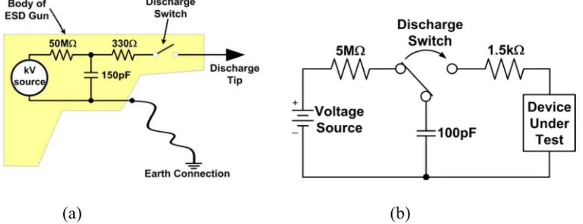
The objective of the standard, IEC 61000-4-2, is to establish a common and reproducible basis for evaluating the performance of CMOS ICs inside the electrical/electronic microelectronic products. This standard specifies typical waveform of the discharge current, test levels, test equipment, test set-up, and test procedure. In order to verify the disturbance of CMOS ICs under system-level ESD tests, the ESD gun is used to zap the ESD-induced energy into the EUT. Fig. 1.1 (a) shows the equivalent circuit of ESD gun. Moreover, the equivalent circuit of the human body model is shown in Fig. 1.1 (b). The energy storage capacitor, the discharge resistor, and the discharge switch shall be placed as close as possible to the discharge electrode. Comparing with the two equivalent circuits, the storage capacitor
~ 4 ~
in system-level ESD test is 150pF, while in component-level ESD test, it is 100pF. That means, the ESD-induced energy stored in the system-level ESD condition is larger than that in the component-level ESD condition. The discharge resistors used in the Fig. 1.1 (a) and (b) are 330 and 1.5k, respectively. Therefore, the ESD-induced energy generating from ESD gun in system-level ESD tests has faster rise time than that in component-level ESD tests. Fig. 1.2 shows the typical waveforms of the discharge current under system-level ESD test (IEC 61000-4-2) and component-level ESD test (MIL-STD 883). Under 8-kV ESD zapping condition, the peak current in system-level ESD test is about five times larger than that in component-level ESD test. In order to compare the test results obtained from different ESD generators, the characteristics of the waveform of discharge current are listed in Table I. Table II shows the test level (test voltage) of component-level ESD test, such as HBM, MM, and CDM. The system-level ESD tests are divided into contact discharge and air discharge test modes, as shown in Table III. The discharge electrodes of two test modes are shown in Fig. 1.3. Contact discharge is the preferred test method, and air discharge shall be used when contact discharge cannot be applied. There is no obvious relationship to imply that the test severity is related between contact discharge and air discharge test modes.
(a) (b)
Fig. 1.1 The equivalent circuit of (a) ESD gun which is used to zap the ESD-induced energy under system-level ESD test and of (b) human body model under component-level ESD test.
~ 5 ~
Fig. 1.2 Under 8-kV ESD zapping, the peak current in system-level ESD test is about five times larger than that in component-level ESD test.
Fig. 1.3 Discharge electrodes of ESD gun which is used under system-level ESD test with (a) contact discharge mode and (b) air discharge mode.
TABLE I Waveform parameters of discharge current.
Level Indicated Voltage (kV) First Peak Current ±10% (A) Rise Time (ns) Current (±30%) at 30ns (A) Current (±30%) at 60ns (A) 1 2 7.5 0.7 to 1 4 2 2 4 15 0.7 to 1 8 4 3 6 22.5 0.7 to 1 12 6 4 8 30 0.7 to 1 16 8
TABLE II Component-level ESD specifications. Model Name Test Voltage Human Body Model >2000V
Machine Model >200V Charge Device Model >1000V
~ 6 ~
TABLE III System-level EMC/ESD specifications - test levels. Contact Discharge Air Discharge
Level Test Voltage (kV) Level Test Voltage (kV)
1 ± 2 1 ± 2 2 ± 4 2 ± 4 3 ± 6 3 ± 8 4 ± 8 4 ± 15 X Specified by Customer X Specified by Customer
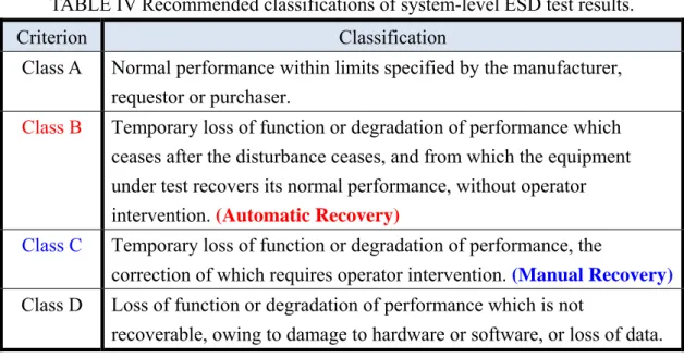
Comparing Table III with Table II, the test voltage of system-level ESD is larger than component-level ESD, whether under contact discharge or air discharge test modes. According to these phenomena, system-level ESD tests affect the system operation of the microelectronic products more seriously than component-level ESD tests.Table IV shows the evaluation of system-level ESD test results. The test results shall be classified in terms of hardware damage, loss function, or degradation of performance of the EUT. From the evaluation table, the microelectronic product should reset itself automatically after system-level ESD test to pass the “class B” specification.
TABLE IV Recommended classifications of system-level ESD test results. Criterion Classification
Class A Normal performance within limits specified by the manufacturer, requestor or purchaser.
Class B Temporary loss of function or degradation of performance which ceases after the disturbance ceases, and from which the equipment under test recovers its normal performance, without operator intervention. (Automatic Recovery)
Class C Temporary loss of function or degradation of performance, the
correction of which requires operator intervention. (Manual Recovery)
Class D Loss of function or degradation of performance which is not
~ 7 ~
The EUT shall be operated within the specified climatic conditions to avoid unnecessary influence from electromagnetic environment of the laboratory. The measurement setup of system-level ESD test is shown in Fig. 1.4 and the elaboration of this setup will be followed in chapter 3.
Fig. 1.4 Measurement instruments of system-level ESD test.
1.2.2. IEC 61000-4-4 Specification
IEC 61000-4-4 is an international standard which gives immunity requirements and test procedures related to electrical fast transients (EFT) [9]. EFT disturbances commonly exist in industrial environment where electromechanical switches are used. The EFT test intends to demonstrate the immunity of electronic equipments against transient disturbances originating from switching transients, such as interruption of inductive loads, relay constant bounce, etc.
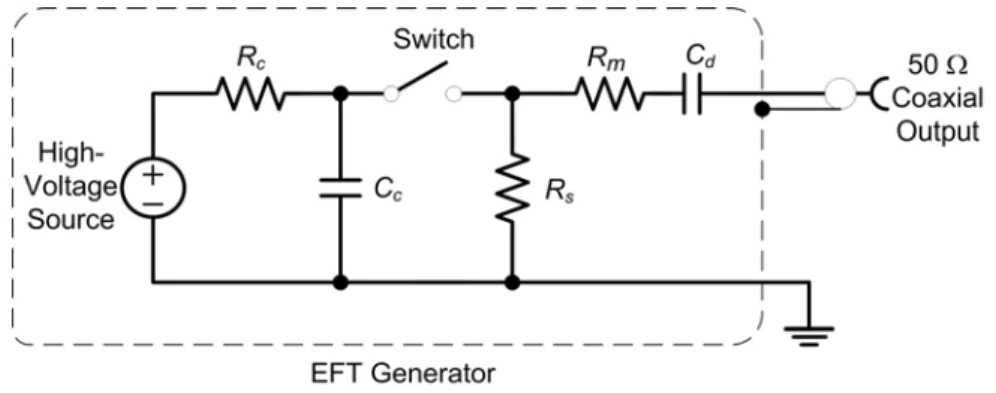
The equivalent circuit diagram of the EFT generator is shown in Fig. 1.5 and the major elements of the EFT test generator are listed in Table V. In particular, the impedance matching resistor Rm (50) and the DC blocking capacitor Cd (10nF) are defined in the standard. The
charging capacitor Cc is used to store the charging energy and Rc is the charging resistor. The
~ 8 ~
Fig. 1.5 The equivalent circuit of EFT generator.
TABLE V Characteristics of the EFT generator. Parameter Definition
Rc Charge Resistor
Cc Energy Storage Capacitor
Rs Duration Shaping Resistor
Rm Impedance Matching Resistor
Cd DC Blocking Capacitor
During EFT tests, the power lines of the CMOS ICs inside the microelectronic products no longer maintain their initial voltage levels. A number of fast transients would randomly couple into power, ground, and I/O pins, causing the ICs inside the EUT to be upset or frozen after EFT zapping. The characteristics of such a high-voltage-level EFT-induced disturbance are listed in Table VI and shown in Fig. 1.6. The test voltage waveforms of these fast transients are defined in the standard with the repetition frequency of 5kHz and 100kHz. A burst consists of 75 pulses with repetition period of 0.2ms (repetition rate of 5kHz) under EFT tests. Therefore, the burst duration time is 15ms, and the period between two adjacent bursts is 300ms. Similarly, for the EFT pulse with the repetition frequency of 100kHz, there are seventy-five pulses in each burst and the burst duration time is 0.75ms. The rise time and duration of a single pulse voltage waveform must accord with the characteristics which are listed in Table VII and shown in Fig. 1.7. A voltage pulse waveform with rise time of 5ns±30% and duration of 50ns±30% occurs on the test pins of EUT under EFT tests.The EFT
~ 9 ~
test levels for testing power supply ports and for testing I/O, data, and control ports of the EUT are listed in Table VIII.The voltage peak for I/O, data, and control ports is half of the voltage peak for testing power supply ports. Level “X” is an open level, and is specified in the dedicated equipment specification.
TABLE VI Characteristics of the fast transient/burst. Repetition
Rate (kHz)
Repetition
Period (ms) Pulse Number
Burst Duration (ms) Burst Period (ms) 5 0.2 75 15 300 100 0.01 75 0.75 400
TABLE VII Characteristics of a single pulse in each burst. Parameter Value
Frequency 5 kHz or 100 kHz Rise Time 5ns ± 30%
Duration 50ns ± 30%
TABLE VIII EFT specifications - test levels.
Level
On Power and PE (Protective Earth) Ports
On I/O (Input/Output) Signal, Data, and Control Ports Voltage Peak (kV) Repetition Rate (kHz) Voltage Peak (kV) Repetition Rate (kHz) 1 0.5 5 or 100 0.25 5 or 100 2 1 5 or 100 0.5 5 or 100 3 2 5 or 100 1 5 or 100 4 4 5 or 100 2 5 or 100 X Specified by Customer Specified by Customer Specified by Customer Specified by Customer
~ 10 ~
Fig. 1.6 General graph of fast transient/burst.
Fig. 1.7 Voltage waveform of a single pulse in each burst.
1.3. Thesis Overview
Based the previous introduction, how to solve the system-level ESD events has become an important issue for the IO industry. The goal of this thesis is to find some chip-level solutions towards system-level ESD problems. This thesis would divide into five chapters.
In chapter 2, an overview of some traditional techniques on solving system-level ESD events is introduced. In chapter 3, by using the device of silicon controlled rectifier (SCR) as memory unit, the on-chip SCR-based transient detection circuit is proposed. In chapter 4, the topic focuses on the 4-bit transient-to-digital converter. Finally, in chapter 5, the conclusions and the future works of this thesis are given.
~ 11 ~
Chapter 2
Solutions to Overcome System-Level Electrical
Transient Disturbance
2.1. Background
The phenomenon of electrostatic discharge commonly exists in the real world. For component-level ESD protection, grounded-gate NMOS (GGNMOS) and diode are the simple way to protect CMOS ICs from ESD events. Moreover, to provide strong protection against transient disturbance, other protection methods and new structure device have been studied and proposed to enhance immunity against large impulse current. However, system-level ESD test is defined when the power line of the microelectronic products connects to the normal operating voltage, which is different from test conditions of component-level ESD tests. Furthermore, as shown in Fig. 1.2, the peak current in system-level ESD test is about five times larger than that in component-level ESD test. The system-level ESD stresses can cause more serious damage compared with component-level ESD events. Therefore, the methods to prevent damages against component-level ESD event may not be available in system-level ESD protection considerations.
Recently, IC designers gradually pay more attentions to the system-level ESD events. More and more test methods have been published to investigate the system-level ESD events. It would provide an appropriate way for IC designers to obtain more analysis ways on the transient disturbance protection. Generally in laboratory tests, the ESD robustness of discrete devices is tested by applying a current pulse with a waveform compliant to the IEC 61000-4-2 standard. The ESD failure threshold is typically determined by monitoring the leakage current.
~ 12 ~
When the leakage current is larger than the defined value, ESD damage is considered to happen [10]. Based on this knowledge, several software, including finding the hot spot on the IC chip, are now popular in the IC industry. A new test standard, which called human metal model (HMM), also comes up to connect the relationship between the component-level ESD and the system-level ESD tests [11]. Although there are lots of ways to do the system-level ESD test, the on-chip solution towards it is still not too much. For traditional solution for microelectronic products against system-level ESD tests, the basic concept is to use off filters to bypass or absorb the large transient disturbance. Since for the advanced technology, system-on-a-chip (SOC) has become a trend to provide multi-function integration and save cost, how to avoid system-level ESD stresses causing SOC system locked in frozen state would become an important design topic
2.2. Traditional System Design Solutions
In order to improve the immunity of microelectronic products to achieve the strict ESD specifications, system designers can take many approaches to prevent ESD damage. One of the system design solution against system-level ESD events is to add some discrete noise-decoupling components or board–level noise filters on the printed circuit board (PCB), as shown in Fig. 2.1. For example, Fig. 2.1(a) shows the system solution to overcome the system-level ESD issue in keyboard, and Fig. 2.1(b) is used for universal series bus (USB) input/output (I/O) port.
~ 13 ~
(a)
(b)
Fig. 2.1 The system solution to overcome the system-level ESD issue by adding extra discrete components to absorb or bypass the electrical fast transients (a) in keyboard and (b) in USB I/O port.
These discrete components are used to decouple, bypass, or absorb the transient noise generated from system-level ESD events. Therefore, the discrete components can reduce the transient energy of transient disturbance coupled on power lines of CMOS ICs inside microelectronic products. Some noise-decoupling components can even clamp the transient voltage at low level to avoid ESD damage on internal circuits of CMOS ICs. Some discrete noise-bypassing components for system-level ESD protection, such as transient voltage suppressor (TVS), or low-pass noise filters, have been reported and would discuss in the following sections [12].
2.2.1. Transient Voltage Suppressor (TVS)
Transient voltage suppressor (TVS) is commonly used to improve the system-level ESD immunity of microelectronic products. It can provide ESD energy discharge path under system-level ESD tests. TVS is located between I/O ports and connected pins of CMOS ICs
~ 14 ~
to provide system-level ESD protection function in the PCB of microelectronic products.The main function of TVS is to absorb high peak power under ESD tests. It is acted as a surge protector.The peak pulse power of TVS can be estimated by
peak pp clamp
P I V (1)
where Ipp is the maximum lightning current that TVS can bypass, and Vclamp is the voltage
when Ipp is applied across the device.Devices with lower clamping voltage during ESD stress
conditions can sustain higher ESD level.Although TVS could be ESD protector,its immunity performance is not well enough compared to other discrete components.Moreover, TVS has high capacitive loading, which can cause distortion on high data rate signals.As a result, TVS is not suitable for high speed applications.
For ESD protections, there are many types of TVS components, such as varistor, metal oxide varistors (MOVs), and zener diode, etcs. Varistors are made of ceramic materials. MOVs contain a ceramic mass of zinc oxide grains. Compare with other TVS components, MOVs have lower capacitance. However, for high speed interface applications, the capacitance of MOVs is still too high to prevent signal distortion.Moreover, MOVs has high impedance with low clamping voltage. When the voltage across this device is high, the resistance value would drop to a low level. This voltage drop across the varistor will dramatically increase as the current increase. As a result, if the ESD clamping voltage is too high, varistor is hard to protect electronic products.
2.2.2. Low-Pass Noise Filter
To meet the strict system-level ESD specification, different types of board-level noise filters have been investigated to improve the immunity of CMOS ICs inside the
~ 15 ~
microelectronic products under system-level ESD tests [13]. Adding board-level noise filter between noise trigger source and CMOS ICs can absorb, bypass, or decouple ESD-generated energy to avoid ESD damage on EUT. Several types of board-level noise filters, such as capacitor filter, LC-like filter (2nd-order), and-section filter (3rd-order), as shown in Fig. 2.2,
have been confirmed the enhancement of system-level ESD immunity. For evaluating the transient-induced latchup (TLU) level of DUT, these three different kinds of filters are investigated. Among different noise filter network, the higher-order noise filters have better performance to enhance TLU-triggered level of DUT, and thus have better immunity against system-level ESD events. Experimental data is shown in Fig. 2.3 [13].
(a) (b) (c)
Fig. 2.2 Board-level noise filter of (a) capacitor filter, (b) LC-like filter, and (c)-section filter.
Fig. 2.3 Relations between the decoupling capacitance and the TLU level of the DUT under three types of noise filter networks: capacitor filter, LC-like filter, and -section filter [13].
~ 16 ~
2.2.3. Design Concept of Printed Circuit Board (PCB)
While discrete ESD components are used to suppress the effect of system-level ESD events, PCB design is another important topic on ESD protection design. A simple diagram was shown in Fig. 2.1. To design the printed circuit board against system-level ESD events, few concepts needs to be taken into account. First, the induced magnetic current into circuit loop will be proportional to the size of the loop [12].Therefore, minimizing the loop size on the PCB is a critical design for ESD reliability enhancement.Second, place the circuit devices on the PCB as close as possible to minimize the lengths of signal and power lines. It can avoid receiving too much energy generating from system-level ESD events.
2.2.4. External Hardware Timer
Another method which is totally different from the previous solutions is to regularly check the system abnormal conditions by using an external hardware timer, such as watch dog timer. This additional hardware timer is often designed with registers or flip flops as a reference clock for system operation if the main program was locked or frozen due to some fault conditions. However, during system-level ESD or EFT tests, the logic states stored in the registers or flip flops of hardware timer would sometimes also be destroyed, still causing malfunction or frozen condition in the system operation. Therefore, this kind of timer is not a stable way to protect microelectronic products against system-level ESD events.
2.3. Hardware/Firmware Co-Design
The above solutions try to solve system-level ESD events by off-chip designs, which would occupy additional chip area. It has been reported that the ESD protection device required more IC area to achieve 2 kV HBM ESD protection when the gate oxide thickness shrinks, as shown in Fig. 2.4 [14].
~ 17 ~
Fig. 2.4 Required IC area for ESD protection as a function of chip size [14].
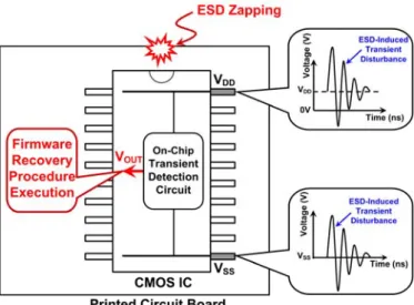
In recent years, it had been reported that the hardware/firmware co-design can effectively improve the system-level ESD susceptibility of the CMOS IC products [8]. As the hardware/firmware co-design case shown in Fig. 2.5, the detection results (VOUT) from the
on-chip transient detection circuit can be temporarily stored as a system recovery index for firmware check. The transient detection circuit is designed to detect and memorize the occurrence of system-level ESD events. For example, the output (VOUT) state in the on-chip
transient detection circuit and the firmware index are initially set to logic “1”. When the fast electrical transient happens, the on-chip transient detection circuit can detect the fast electrical transient and then change the output state (VOUT) from logic “1” to logic “0”. The system
recovery index is therefore flagged at logic “0”, which will be checked by the firmware to automatically recover all system functions to a stable state as soon as possible. After the recovery procedure, the output state of the on-chip transient detection circuit and the firmware index are re-set to logic “1” again for detecting the next electrical transient disturbance events.
~ 18 ~
Fig. 2.5 Hardware/firmware co-design for system recovery by using the detection results of the on-chip transient detection circuit.
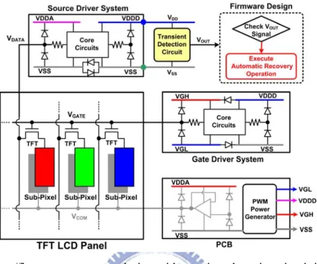
Moreover, it had been proven that the hardware/firmware co-design can effectively improve the robustness of the industrial products against electrical transient disturbance [8]. For display system protection design with thin-film transistor (TFT) liquid crystal display (LCD) panel, multiple power systems are needed for electrical display functions, as shown in Fig. 2.6.For example, in the backside of source driver IC, the analog power line (VDDA) is used for digital-to-analog converter circuit and digital power line (VDDD) is used for shifter register to store display signals. The transient detection circuit, designed for detecting and memorizing the occurrence of ESD-induced transient disturbance, can connect with VDDD power line to implement the hardware/firmware protection design in display system. The detection results from the detection circuit can be temporarily stored as a system recovery index for firmware check, as shown in Fig. 2.6. In the beginning, the output (VOUT) state of
the detection circuit is initially reset to logic “1.” When the electrical transients happen, the detection circuit can detect the occurrence of system-level ESD-induced transient disturbance and transit the output state (VOUT) to logic “0.” At this moment, the firmware index is also
changed to logic “0” to initiate automatic recovery operation to restore the microelectronic display system to a desired stable state as soon as possible. After the automatic recovery
~ 19 ~
operation, the output of the detection circuit and the system recovery index are re-set to logic “1” again for detecting the next ESD-induced electrical transient disturbance events.
Fig. 2.6 Hardware/firmware system co-design with transient detection circuit in display panel product.
2.4. Summary
System-level ESD protection has now become more and more important for IC industry. Several methods have been discussed and analyzed in this chapter. Transient voltage suppressor can provide ESD energy discharge path under system-level ESD tests, but its nonlinear resistance characteristic is its drawback. Board-level noise filter on PCB is another choice to enhance system-level immunity, but the occupied area should be taken into account as well. Above all, traditional solutions toward system-level ESD immunity have some limitation, either in the aspect of occupied area or cost. Hardware/firmware co-design has been proved to have capability enhancing the system-level ESD robustness of microelectronic products. Moreover, on-chip detection circuit can be used to save PCB area and provide detection results for firmware to execute the automatic system recovery procedures. Based on
~ 20 ~
this request, the on-chip solutions will be developed in advance and to be the trend for future solution for system-level ESD events.
~ 21 ~
Chapter 3
Design of On-Chip SCR-Based Transient Detection
Circuit
3.1. Background
It has been investigated that during the system-level ESD events, the power line and ground line of the microelectronic products would be disturbed by the fast and large transient electrical disturbance. As technology continues to scale down, designers should put more emphasis on the electrical disturbance generated from system-level ESD stresses, which would cause malfunction of CMOS ICs. Traditional board-level solutions have limitation in silicon integration and product cost. According to the IEC61000-4-2 standard, IC product is recommended to pass “class B” at least. That means, system should have the capability to automatically recover from upset states after the ESD zapping, not stay in the frozen or any unknown state. In recent years, on-chip transient detection has proposed to co-operate with hardware/firmware system to execute the system auto recovery procedures. With the published experimental results, it has been confirmed that chip-level co-design can successfully improve system-level ESD immunity and save ESD protection device area.
3.2. Prior Art
Previously, four transient detection circuits for system-level ESD protections have been proposed [8], [15]-[17]. The circuit diagram of the first on-chip transient detection circuit is shown in Fig. 3.1 (a). Two latch logic gates are used as the ESD sensor unit to detect the system-level ESD events on the power and ground lines. Coupling capacitors can be added
~ 22 ~
between the input/output nodes of latch and VDD/VSS lines in order to enhance the sensitivity
of the ESD sensor to fast transients on the VDD/VSS line.It has been analyzed that the NMOS
in the inverter of sensor_1 in Fig. 3.1 (a) is designed with a larger W/L ratio than that of the PMOS to make the latch locking at logic “0” easily. The PMOS in the inverter of sensor_2 is designed with a larger W/L ratio than that of the NMOS to make the latch easily locking at logic “1” [8].
The second transient detection circuit is designed with latch logic gates and capacitors shown in Fig. 3.1 (b). In this transient detection circuit, a latch circuit composed of two inverters is used to memorize the logic state after the system-level ESD tests.The capacitors Cp1 (Cp2) are used to detect the positive (negative) fast electronic transients. It has been
confirmed that the W/L ratio of inverters in the latch and the coupling capacitance will strongly influence the sensitivity of this detection circuit. The NMOS (Mnr) can provide a
reset function toset the VOUT to be logic “0”.When the voltage of VDD is below the voltage of
VSS, the parasitic diodes of PMOS would be turned on. Therefore, this circuit can detect the
positive system-level ESD events.Similarly, the parasitic diodes of NMOS of inverters would be turned on under the negative system-level ESD stress.
The third one is designed with RC-based circuit structure to realize the transient detection circuit, as shown in Fig. 3.1(c). The two inverter latch is used to memorize the logic state before and after the system-level ESD events. The NMOS (Mnr) provides the reset
function to set the output (VOUT) logic state to be initially high. Under system-level ESD
stress, due to RC time constant delay, the PMOS device of INV_1 and NMOS (Mn1) would be
turned on by the overshooting ESD voltage. Mn1 can pull down the output voltage level and
thus change the output logic state from logic “1” to logic “0”. Therefore, the third proposed transient detection can successfully detect and memorize the occurrence of system-level ESD events.
~ 23 ~
detection function, as shown in Fig. 3.1(d). The PMOS device (Mp1) helps to memorize the
logic state before and after the system-level ESD stress. The NMOS device (Mnr) provides the
reset function to set the initial output voltage (VOUT) to be 0 V. When there is fast electrical
transient disturbance, RC-time constant delay would urge PMOS device (Mp1) to turn on by
the overshooting ESD voltage. Therefore, output logic state would transfer from logic “0” to logic “1”. Those previous transient detection can detect and memorize the occurrence of system-level ESD events.
(a) (b)
(c) (d) Fig. 3.1 Previous transient detection circuits composed of (a) a sensor circuit, (b) a latch
circuit with additional capacitors (CP1 and CP2), (c) RC-based detection cell, and (d) RC
circuit without latch cell.
3.3. New On-Chip SCR-Based Transient Detection Circuit
The new on-chip SCR-based transient detection circuit is designed to detect the positive or negative fast electrical transients during the system-level ESD or EFT tests. Under the normal circuit operation condition (VDD=3.3 V), the output state of the new proposed on-chip
~ 24 ~
SCR-based transient detection circuit is kept at 3.3 V as logic “1”. After the transient disturbance, the output state will transit from 3.3 V to 0 V. Therefore, the new proposed on-chip SCR-based transient detection circuit can detect and memorize the occurrence of system-level electrical transient disturbance events.
3.3.1. Silicon Controlled Rectifier (SCR)
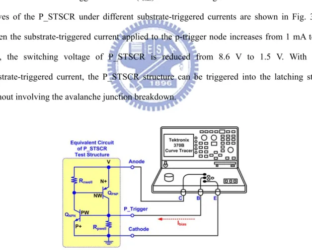
The silicon controlled rectifier (SCR) was often used as the on-chip ESD protection device due to its high ESD robustness within small layout area [18]. The anode of SCR is connected to the P+ and N+ diffusions in N-well (NW), whereas the cathode of SCR is connected to the N+ and P+ diffusions in P-well (PW). The equivalent circuit of the SCR structure composes of a lateral NPN and a vertical PNP bipolar transistor to form the 2-terminal/4-layer PNPN (P+/NW/PW/N+) structure. The original switching voltage of the SCR device is decided by the avalanche breakdown voltage of the N-well/P-well junction. It has been reported that the turn-on mechanism of SCR device is essentially a current triggering event [19]. While a current is applied to the base or substrate of SCR device, it can be quickly triggered into its latching state. The device cross-sectional view and the layout top view of the p-type substrate-triggered SCR (P_STSCR) are shown in Fig. 3.2(a) and Fig. 3.2(b), respectively.
(a) (b)
Fig. 3.2 (a) Device cross-sectional view and (b) layout top view, of the p-type substrate-triggered SCR (P_STSCR).
~ 25 ~
An extra P+ diffusion is inserted into the P-well of the P_STSCR device and connected out as the p-trigger node. The geometrical parameters such as D and W represent the distance between the anode and cathode, and the distance between the adjacent well contacts, respectively. In this work, the P_STSCR structure with the layout parameters of D=0.86m and W=3.8 m in a 0.18-m CMOS process with 3.3-V devices is used as the memory unit to memorize the occurrence of electrical transient disturbance. The SCR in this work is not used as on-chip ESD protection device, but as the memory unit in the transient detection circuit.
The setup to measure the DC current–voltage (I-V) curves of the fabricated P_STSCR device under substrate-triggered current (Ibias) is shown in Fig. 3.3. The measured DC I-V
curves of the P_STSCR under different substrate-triggered currents are shown in Fig. 3.4. When the substrate-triggered current applied to the p-trigger node increases from 1 mA to 4 mA, the switching voltage of P_STSCR is reduced from 8.6 V to 1.5 V. With the substrate-triggered current, the P_STSCR structure can be triggered into the latching state without involving the avalanche junction breakdown.
~ 26 ~
Fig. 3.4 The measured I-V characteristics of P_STSCR device under different trigger currents.
3.3.2. SCR-Based Transient Detection Circuit
The new proposed on-chip SCR-based transient detection circuit of this work is shown in Fig. 3.5. The P_STSCR device shown in Fig. 3.2 is used as the memory unit to memorize of the occurrence of system-level electrical transient disturbance. The anode of P_STSCR is connected to the drain of PMOS (Mpr) device. The gate of PMOS (Mpr) is connected to VSS by
the initial reset signal (VRESET) to set the initial output voltage (VOUT2) at 3.3 V. The RC-delay
circuit and the inverter are designed to provide the SCR triggering current. Under the system-level ESD or EFT events, the transient voltage has a fast rise time in the order of nanosecond (ns). Because the RC-delay circuit is designed with a time constant in the order of microsecond (s), the voltage level of VX has much slower voltage response than the transient
voltage coupling to VDD.Due to the longer delay of the voltage increase at the node VX, the
PMOS device (Mp1) can be turned on by the overshooting voltage at VDD and conduct trigger
current to the p-trigger node. The SCR device is therefore turned on to pull down the output voltage (VOUT1) level to the SCR holding voltage of ~1.2 V. In the two-inverter buffer stage,
the logic threshold voltage of inverter1 (INV_1) is designed at ~2.4 V and that of inverter2 (INV_2) is ~1.7 V. Therefore, after electrical transient disturbance, the final output voltage (VOUT2) of the proposed detection circuit will change from 3.3 V to 0 V to detect and
~ 27 ~
Fig. 3.5 The new proposed on-chip SCR-based transient detection circuit. The P_STSCR is used as memory cell to memorize the occurrence of electrical transient disturbance.
memorize the occurrence of system-level ESD/EFT-induced transient disturbance. The reset function (VRESET) is then used to release the turn-on state of SCR device by turning off
Mpr_device, and reset the output voltage (VOUT2) back to 3.3 V again for detecting the next
system-level transient disturbance.
3.4. Experimental Results
The proposed detection circuit has been designed and fabricated in a 0.18-m CMOS process with 3.3-V devices. The fabricated test chip with the silicon area of 542 m x 240 m is shown in Fig. 3.6.
Fig. 3.6 Chip photo of the new proposed on-chip SCR-based transient detection circuit fabricated in a 0.18-m CMOS process with 3.3-V devices.
~ 28 ~
3.4.1. Transient-Induced Latchup (TLU) Test
To evaluate the system-level ESD immunity of a single IC inside the equipment under test (EUT), a component-level transient-induced latchup (TLU) measurement setup was reported with the following two advantages [20]. First, the TLU immunity of a single IC can be evaluated by the measured voltage and current waveforms through the oscilloscope. Second, with the ability of generating an underdamped sinusoidal voltage, it can accurately simulate how an IC inside the EUT is disturbed by the ESD-generated transient disturbance during the system-level ESD test. Fig. 3.7 illustrates such a component-level TLU measurement setup. A charging capacitance of 200pF is used to store the charges as the TLU-triggering source, VCharge, and then the stored charges are discharged to the device under
test (DUT) through the relay. The underdamped sinusoidal voltage generated by TLU measurement is similar to the transient voltage on the power pins of CMOS ICs under the system-level ESD tests, whether polarity (positive or negative) of the ESD voltage is. Moreover, a small current-limiting resistance of 5 is recommended to protect the DUT from electrical-over-stress (EOS) damage during the high-current (low-impedance) latching state. The supply voltage of 3.3 V is used as VDD and the trigger source is directly connected to
DUT through the relay in the TLU measurement setup.
~ 29 ~
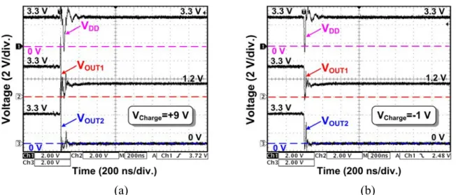
Figs. 3.8(a) and 3.8(b) show the measured VDD, VOUT1, and VOUT2 transient voltage
waveforms of the on-chip SCR-based transient detection circuit under the TLU tests with VCharge of +9 V and -1 V, respectively. As shown in Fig. 3.8(a), under the TLU test with VCharge
of +9 V, VDD begins to increase rapidly from 3.3 V with positive-going underdamped
sinusoidal voltage waveform. During the TLU test, VOUT1 and VOUT2 are influenced
simultaneously by the positive-going underdamped sinusoidal voltage coupled to VDD power
line. After the TLU test with the VCharge of +9 V, the output voltage VOUT1 of the proposed
transient detection circuit is changed from 3.3 V to 1.2 V, which is equal to the SCR holding voltage. Through two-inverter buffer stage, VOUT2 of the proposed detection circuit is pulled
down to 0 V. In Fig. 3.8(b), under the TLU test with VCharge of -1 V, VDD begins to decrease
rapidly from 3.3 V with negative-going underdamped sinusoidal voltage waveform. During this TLU test, VOUT1 and VOUT2 are influenced simultaneously by the negative-going
underdamped sinusoidal voltage coupled to VDD power line. After the TLU test with the
VCharge of -1 V, the VOUT2 of the proposed transient detection circuit also transits from 3.3 V to
0 V.
From the TLU test results, the proposed on-chip SCR-based transient detection circuit can successfully memorize the occurrence of electrical transients. With positive or negative underdamped sinusoidal voltages coupled to VDD power line, the output voltage (VOUT2) of
the proposed on-chip SCR-based transient detection circuit can be changed from logic “1” to logic “0” after TLU tests.
~ 30 ~
(a) (b)
Fig. 3.8 Measured VDD, VOUT1, and VOUT2 waveforms on the on-chip SCR-based transient
detection circuit under TLU tests with the VCharge of (a) +9 V and (b) -1 V.
3.4.2. System-Level ESD Test
In IEC 61000-4-2, two test modes have been specified, which are the air-discharge and contact-discharge test mode. In the case of contact discharge test mode, the sharp discharge tip is used to simulate the mechanical ESD damage on the EUT. The contact discharge is applied to the conductive surfaces of the EUT (direct application) or to the coupling planes (indirect application). Contact discharge is further divided into direct discharge to the system under test, and indirect discharge to the horizontal or vertical coupling planes. Fig. 3.9 shows the measurement setup of the system-level ESD test standard with indirect contact-discharge test mode. The measurement setup of system-level ESD test consists of a wooden table on the grounded reference plane (GRP). In addition, an insulation plane is used to separate the EUT from the horizontal coupling plane (HCP). The HCP are connected to the GRP with two 470 k resistors in series [6]. When the ESD gun zaps the HCP, the electromagnetic interference (EMI) coming from ESD gun will be coupled into all CMOS ICs inside EUT. The power lines of CMOS ICs inside EUT will be disturbed by the ESD-coupled energy.
~ 31 ~
Fig. 3.9 Measurement setup for system-level ESD test with indirect contact-discharge test mode [6] to evaluate the detection function of the on-chip SCR-based transient detection circuit.
With such measurement setup, the circuit function of the proposed detection circuit after system-level ESD tests can be evaluated. By monitoring the oscilloscope, the transient responses on power lines of CMOS ICs can be recorded and analyzed. Before each system-level ESD test, the initial output voltages (VOUT1 and VOUT2) of the proposed detection
circuit are all reset to 3.3 V. After each system-level ESD test, the output voltages (VOUT1 and
VOUT2) are monitored to check their final voltage levels. Thus, the function of the proposed
detection circuit can be evaluated under system-level ESD tests.
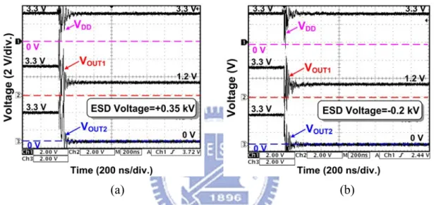
The measured VDD, VOUT1, and VOUT2 waveforms of the proposed detection circuit under
system-level ESD test with the ESD voltage of +0.35 kV zapping on the HCP are shown in Fig. 3.10(a). VDD begins to rapidly increase from the normal voltage level of 3.3 V.
Meanwhile, VOUT1 and VOUT2 begin to change under such a high-energy ESD stress. During
the fast transient disturbance, VDD, VOUT1, and VOUT2 are influenced simultaneously. Finally,
VOUT1 is pulled down to 1.2 V. Through buffer stages, VOUT2 of the proposed detection circuit
transits from 3.3 V to 0 V.
The measured VDD, VOUT1, and VOUT2 waveforms of the proposed detection circuit under
~ 32 ~
3.10(b). During the ESD-induced transient disturbance, VDD begins to decrease rapidly from
the original voltage level of 3.3 V. Finally, the output voltage (VOUT2) of the proposed
transient detection circuit is changed from 3.3 V to 0 V.
Therefore, the new proposed on-chip SCR-based transient detection circuit can successfully detect the electrical transients under system-level ESD tests with positive or negative ESD voltages.
(a) (b)
Fig. 3.10 Measured VDD, VOUT1, and VOUT2 transient voltage waveforms of the on-chip
SCR-based transient detection circuit under system-level ESD tests with ESD voltage of (a) +0.35 kV and (b) -0.2 kV.
3.4.3. Electrical Fast Transient (EFT) Test
The measurement setup for EFT test combined with attenuation network is shown in Fig. 3.11. EFT generator is connected to the DUT with VDD of 3.3 V through the attenuation
network. In order to simulate the degraded EFT-induced transient disturbance on CMOS ICs inside the microelectronic products, the attenuation network with -40 dB degradation is used in this work. The amplitude of EFT-induced transients can be adjusted by the attenuation network.
~ 33 ~
Fig. 3.11 Measurement setup for EFT test combined with attenuation network [9].
Figs. 3.12(a) and 3.12(b) show the measured VDD, VOUT1, and VOUT2 transient responses
of the proposed detection circuit under the EFT tests with input EFT voltages of +750 V and -400 V, respectively. As shown in Fig. 3.12(a), under the EFT test with positive voltage of +750 V, VDD begins to increase rapidly from 3.3 V with positive exponential voltage pulse.
During the EFT test, VOUT1 and VOUT2 are influenced simultaneously by the positive
exponential voltage pulse coupled to VDD power line. After the +750-V EFT test, the output
voltage VOUT1 (VOUT2) of the proposed detection circuit transits from 3.3 V to 1.2 V (0 V). In
Fig. 3.12(b), under the EFT test with negative voltage of -400 V, VDD begins to decrease
rapidly from 3.3 V with negative exponential voltage pulse. After the EFT test, the output voltage VOUT2 of the proposed detection circuit transits from logic “1” to logic “0”.
From the EFT test results shown in Figs. 3.12(a) and 3.12(b), either positive or negative EFT voltages coupled to VDD power line, the output voltage (VOUT2) of the proposed detection
circuit can be changed from 3.3 V to 0 V. Therefore, the new proposed on-chip SCR-based transient detection circuit can successfully memorize the occurrence of EFT-induced exponential pulse transient disturbance.
~ 34 ~
(a) (b)
Fig. 3.12 Measured VDD, VOUT1, and VOUT2 waveforms on the on-chip SCR-based transient
detection circuit under EFT tests with (a) +750-V and (b) -400-V EFT voltages combined with attenuation network.
3.5. Summary
A new on-chip SCR-based transient detection circuit to detect system-level electrical transient disturbance has been implemented in a 0.18-m CMOS process with 3.3-V devices. By using P_STSCR device and RC-delay circuit, the proposed detection circuit is designed to detect fast electrical transients during the system-level ESD or EFT tests. Experimental results in silicon chip have successfully verified that the proposed detection circuit can successfully memorize the occurrence of electrical transients under system-level ESD or EFT tests. From the previous research, it is reasonable that with hardware/firmware co-design method, the output state of the proposed on-chip SCR-based transient detection circuit can be used as the firmware index to provide an effective solution against the system malfunction caused by system-level electrical transient disturbance.

![Fig. 3.11 Measurement setup for EFT test combined with attenuation network [9].](https://thumb-ap.123doks.com/thumbv2/9libinfo/8249680.171648/46.892.265.673.107.347/fig-measurement-setup-eft-test-combined-attenuation-network.webp)
