Deposition of Mesoporous Silicon Carbide Thin Films from
(Me
3Si)
4Sn: Tin Nanoparticles as in Situ Generated Templates
Chia-Hsin Wang,
†Wen-Yih Shen,
†Pei-Sun Sheng,
†Chi-Young Lee,
‡and Hsin-Tien Chiu
†,*
Department of Applied Chemistry, National Chiao Tung UniVersity, Hsinchu,
Taiwan, 30050, Republic of China, and Department of Materials Science and Engineering and Center for Nanotechnology, Materials Science and Microsystems, National Tsing Hua UniVersity,
Hsinchu, Taiwan, 30043, Republic of China
ReceiVed April 18, 2007. ReVised Manuscript ReceiVed September 6, 2007
With use of Sn(SiMe3)4as the precursor, amorphous SiC1+xthin films with Sn nanoparticles embedded were grown on Si substrates at 923 K by low-pressure chemical vapor deposition. After treatment under hydrogen plasma at 923 K, the Sn nanoparticles in the films were removed by an HF solution and by evaporation at 1423 K. Following the removal of Sn, high-temperature treatments at 1273-1423 K converted the amorphous thin films into mesoporous semiconductingβ-SiC thin films with pore sizes 10-100 nm.
1. Introduction
In nature and the laboratory, the morphology and structure of many objects are shaped and altered mainly by phase segregation. Interactions among different domains of the constituents may perform cooperatively as hard and soft templates. The effects can be observed in systems such as the formation of minerals,1block copolymers,2and nanosized inorganic and organic structures.3-5In this report, we wish to discuss how to fabricate mesoporous silicon carbide thin films on silicon substrates based on this methodology. Silicon carbide is an excellent semiconductor material for high-temperature, high-power, and high-frequency applications in harsh environments.6,7Recently, many new routes have been developed to prepare silicon carbide nanostructures and thin films. These include solid-state carbothermal reduction of silica, solution-phase sol-gel synthesis and preceramic processes,andvariouschemicalvapordepositiontechniques.3,8-18
Porous silicon carbide thin films on SiC or Si are potentially useful for luminescence and sensing devices.19,20 To date, electrochemical etching of SiC in HF(aq)is the only method to fabricate it into the porous form.19-21However, the route may not be suitable for the fabrication of porous SiC layers onto Si wafers because the high reactivity of Si toward the HF electrolyte would cause preferential dissolution of the substrate.22Porous SiC powders prepared by carbothermal reduction are also difficult to integrate into the device fabrication process.16-18Clearly, a new method is needed to overcome the difficulty. Here, we demonstrate the integration of a metal-organic chemical vapor deposition (MOCVD) process and a phase segregation strategy to achieve this goal.
* Corresponding author. Fax: 886-3-5723764. Tel.: 886-3-5131514. E-mail: [email protected].
†National Chiao Tung University. ‡National Tsing Hua University.
(1) (a) Brian, J.; Charles, F. K. J. Sed. Petrol. 1993, 63, 1018. (b) Guillaume, C.; Olivier, B.; Christophe, D.; Michel, A.; Eric, P. V. Catena 2005, 59, 1.
(2) (a) Muthukumar, M.; Ober, C. K.; Thomas, E. L. Science 1997, 277, 1225. (b) Fo¨rster, S.; Plantenberg, T. Angew. Chem., Int. Ed. 2002, 41, 688.
(3) Wang, C.-H.; Chang, Y.-H.; Yen, M.-Y.; Peng, C.-W.; Lee, C.-Y.; Chiu, H.-T. AdV. Mater. 2005, 17, 419.
(4) (a) Huang, C.-H.; Chang, Y.-H.; Lee, C.-Y.; Chiu, H.-T. Langmuir 2006, 22, 10. (b) Yen, M.-Y.; Chiu, C.-W.; Hsia, C.-H.; Chen, F.-R.; Kai, J.-J.; Lee, C.-Y.; Chiu, H.-T. AdV. Mater. 2003, 15, 235. (c) Hsia, C.-H.; Yen, M.-Y.; Lin, C.-C.; Chiu, H.-T.; Lee, C.-Y. J. Am. Chem. Soc. 2003, 125, 9940.
(5) (a) Chen, F.; Liu, M. Chem. Commun. 1999, 1829. (b) Kyotani, T.; Ma, Z.; Tomita, A. Carbon 2003, 41, 1451. (c) Ramesh, P.; Kishi, N.; Sugai, T.; Shinohara, H. J. Phys. Chem. B 2006, 110, 130. (d) Valle´, K.; Belleville, P.; Pereira, F.; Sanchez, C. Nat. Mater. 2006, 5, 107.
(6) Fissel, A.; Schroter, B.; Richter, W. Appl. Phys. Lett. 1995, 66, 3182. (7) Spetz, A. L.; Baranzani, A.; Tobias, P.; Lundstro¨m, I. Phys. Status
Solidi A 1997, 162, 493.
(8) (a) Shin, Y.; Wang, C.; Exarhos, G. J. AdV. Mater. 2005, 17, 73. (b) Li, Y.; Bando, Y.; Golberg, D. AdV. Mater. 2004, 16, 93.
(9) Hatakeyama, F.; Kanzaki, S. J. Am. Ceram. Soc. 1990, 73, 2107. (10) Seog, I. S.; Kim, C. H. J. Mater. Sci. 1993, 28, 3227.
(11) (a) Yajima, S.; Hayasht, J.; Hasegawa, Y.; Iimura, M. J. Mater. Sci. 1978, 13, 2569. (b) Hasegawa, Y.; Iimura, M.; Yajima, S. J. Mater.
Sci. 1980, 15, 720. (c) Hasegawa, Y.; Okamura, K. J. Mater. Sci. 1983, 18, 3633.
(12) Kamlag, Y.; Goossens, A.; Colbeck, I.; Schoonman, J. Chem. Vap. Deposition 2003, 9, 125.
(13) Chiu, H.-T.; Huang, S.-C. J. Mater. Sci. Lett. 1993, 12, 537. (14) Pitcher, M. W.; Joray, S. J.; Bianconi, P. A. AdV. Mater. 2004, 16,
706.
(15) (a) Liu, Q.; Wu, H.-J.; Lewis, R.; Maciel, G. E.; Interrante, L. V. Chem. Mater. 1999, 11, 2038. (b) Cheng, Q.-M.; Interrante, L. V.; Lienhard, M.; Shen, Q.; Wu, Z. J. Eur. Ceram. Sci. 2005, 25, 233. (16) Sonnenburg, K.; Adelhelm, P.; Antonietti, M.; Smarsly, B.; No¨ske,
R.; Strauch, P. Phys. Chem. Chem. Phys. 2006, 8, 3561.
(17) Lu, A.-H.; Schmidt, W.; Kiefer, W.; Schu¨th, F. J. Mater. Sci. 2005, 40, 5091.
(18) Krawiec, P.; Geiger, D.; Kaskel, S. Chem. Commun. 2006, 2469. (19) Matsumoto, T.; Takahashi, J.; Tamaki, T.; Futagi, T.; Mimura, H.;
Kanemitus. Y. Appl. Phys. Lett. 1994, 64, 226.
(20) (a) Connolly, E. J.; O’Halloran, G. M.; Pham, H. T. M.; Sarro, P. M.; French, P. J. Sens. Actuators A 2002, 99, 25. (b) Connolly, E. J.; Timmer, B.; Pham, H. T. M.; Groeneweg, J.; Sarro, P. M.; Olthuis, W.; French, P. J. Sens. Actuators B 2005, 109, 44.
(21) (a) Shor, J. S.; Grimberg, I.; Weiss, B.; Kurtz, A. D. Appl. Phys. Lett. 1993, 62, 2836. (b) Rittenhouse, T. L.; Bohn, P. W.; Adesida, I. Solid
State Commun. 2003, 126, 245. (c) Rittenhouse, T. L.; Bohn, P. W.; Hossain, T. K.; Adesida, I.; Lindesay, J.; Marcus, A. J. Appl. Phys. 2004, 95, 490.
(22) Takazawa, A.; Tamura, T.; Yamada, M. Jpn. J. Appl. Phys. 1993, 32, 3148.
10.1021/cm0710498 CCC: $37.00 © 2007 American Chemical Society
We show that preceramic amorphous SiC1+x thin films containing Sn nanoparticles can be deposited on Si substrates employing Sn(SiMe3)4as the precursor. After the Sn nano-particles are removed, the SiC1+xfilms are processed further into mesoporous semiconductingβ-SiC thin films.
2. Experimental Section
2.1. Materials. The materials used in the present work included trimethylchlorosilane (Aldrich), lithium ribbon (Aldrich, 99.9%), tin(IV) chloride (Aldrich), hydrofluoric acid (Aldrich, 48%), tetrahydrofuran (Echo Chemical, HPLC-grade), acetone (Echo chemical, HPLC-grade), 1,1,1-trichloroethane (Echo Chemical), buffered hydrofluoric acid (BOE) solution (Echo Chemical), n-type silicon (100) wafer (1-10Ω·cm), and p-type silicon (111) wafer (7-30Ω·cm). The MOCVD precursor Sn(SiMe3)4was synthesized using a literature route.23
2.2. Growth of Sn/Amorphous SiC1+x Thin Films, I. The MOCVD experiments were performed in a hot-wall reactor composed of a Lindberg 55342-4 horizontal tube furnace and a 27 mm diameter quartz tube shown in Figure 1. Radio frequency (rf) power (13.56 MHz) was applied to the reactor through two pieces of copper foil electrodes. After the cleaned Si wafers (1 cm× 1 cm) were placed inside the reactor, they were further treated by H2 plasma (40 sccm, 20 W, 66.7 Pa) at 923 K for 10 min to create a surface favorable to thin film deposition. Sn(SiMe3)4(0.5 g) was evaporated into the reactor at 333 K and 26.7 Pa under the assistance of a constant flow of H2(20 sccm). The deposition was carried out at 923 K for 6 h to grow dark green thin films (I) on the wafers. 2.3. Preparation of Samples I-P, I-P-HF, II, III, and IV. Further processing of I by H2plasma (20 sccm, 10 W) at 923 K for 6 h followed by dipping into HF(aq)(48%) for 30 min generated I-P and I-P-HF, respectively. Then, it was annealed at 1273 K for 1 h to produce II. On the other hand, I-P and I were annealed at 1423 K for 1 h to produce III and IV, respectively.
2.4. Preparation of n-Typeβ-SiC/p-Type Si Heterojunction.
A precursor film I was deposited at 923 K for 90 min on p-type Si (7-30Ω·cm) via the MOCVD process described above. After the film was directly annealed at 1423 K to remove Sn particles embedded inside, IV was prepared. P was doped into the film IV by ion implantation (5× 10¹⁴P3+/cm2at 25 keV) using a Varian E500HP implanter.
2.5. Characterization. Scanning electron microscopic (SEM) and energy dispersive X-ray (EDX) data were collected using a JEOL JSM-6330F at 15 kV. Transmission electron microscopic (TEM) and selected area electron diffraction (SAED) images were obtained on a JEOL JEM-2010 at 200 kV. Thin films peeled off from the Si wafers either by treating them in HF(aq)or due to poor adhesion were collected for TEM characterizations. X-ray diffrac-tion (XRD) studies were carried out using a Bruker AXS D8 ADVANCE diffractometer using Cu KR1radiation. Fourier trans-form infrared (FT-IR) spectra were carried out using a Perkin-Elmer
Spectrum One. Gas chromatography-mass spectrometry (GC-MS) data of volatile byproducts trapped at 77 K were measured using a HP 5890 series II (GC) coupled to a Micromass TRIO-2000 and a JEOL JMS-D100. On-line residual gas analysis (RGA) was obtained from a VG Quadrupoles Sensorlab 300D mounted to the reactor. Raman spectra of the samples were measured by using a Jabin Yvon T-64000 equipped with an Ar+ laser (514.5 nm) and a triple monochromator. X-ray photoelectron spectroscopic (XPS) measure-ments were carried out using a Perkin-Elmer PHI-1600 spectrometer with Mg KR (1253.6 eV) radiation. Electron probe X-ray mi-croanalysis (EPMA) data were measured from JEOL JXA-8500F. Secondary ion mass spectrometry (SIMS) was carried out using a Cameca IMS-4f instrument.
Connection of Cu wires to the thin films and wafers was made by applying silver paste to form the contacts followed by heating in an oven at 383 K for 30 min. The I-V characteristics of the thin films were measured with a Keithley 2400 (DC ( 5 V) by the two-point probe method. The sheet resistance of the films was determined by the four-point probe method using a CMT-SR 2000 N.
3. Results and Discussion
3.1. Growth and Characterization of Sn/Amorphous SiC1+xThin Films. The precursor Sn(SiMe3)4was vaporized at 333 K into a horizontal hot-wall MOCVD reactor (Figure 1) at 923 K to grow thin films on Si substrates. Starting from the precursor inlet, nine pieces of Si wafers were placed at a distance of 5 cm apart inside the reactor. The substrates were numbered from 1 to 9; the number 1 substrate was at the most upstream position, close to the end of the heated zone, while the number 9 substrate was at the reactor center. Initially, thin films were grown on all of the substrates so that better deposition locations inside the reactor could be chosen. Starting from sample 1, the physical appearance of the films ranged from gray, to dark green with silvery white spots, to dark green, and then to black.
From SEM studies, the morphology and thickness of the films were obtained. From the thickness, the corresponding film growth rates at these positions were estimated to be 0.4-24 nm/min. EPMA and EDX spectra showed that all of the samples contained various amounts of Sn, Si, and C. As shown in the EPMA data in Figure 2, this ranges from 44.5 at. % of Sn, 26.7 at. % of Si, and 28.8 at. % of C for sample 2 to 21.7 at. % of Sn, 33.5 at. % of Si, and 44.8 at. % of C for sample 6. Reliable EPMA data were not collected for samples 1, 7, 8, and 9 because the films were not thick enough to avoid the Si signal from the substrate below. For all samples, XRD studies showed reflections from Sn metal only. This suggests that the metal was phase-segregated from an amorphous composite containing Si and C. Since we wished to employ films with reasonable growth rates, smooth surface, and balanced distribution of Sn and the amorphous Si/C composite, we selected samples 3-5, which were dark green in appearance, for the proposed study. These samples are denoted as sample I in the discussion below. This sample and the ones processed from it are summarized in Table 1. The rest of the samples, grown at the positions 1, 2, and 6-9 did not fit the selection criteria for further processing because they were too thin, too high or low in Sn content, and/or contained a high quantity of large-sized particles. (23) Burger, H.; Goetze, U. Angew. Chem., Int. Ed. 1968, 7, 212.
The typical surface morphology of I, characterized by SEM, is displayed in Figure 3A. The elemental composition of I, determined by EDX, is shown in the inset of Figure 3A. It indicates that I contains Sn, Si, C, and traces of O. The EPMA data in Figure 2 show that the sample contained 33.6, 29.0, and 37.4 at. % of Sn, Si, and C, respectively. A representative XRD pattern of I, as shown in Figure 3B, can be indexed to Sn metal (JCPDS, No. 04-0673).24The mean crystallite size of the metal is estimated to be 21.3 nm. This was calculated from the Scherrer equation by using the width data of the Sn(200) reflections. XPS studies showed two binding energies of Sn 3d5/2 electrons at 486.9 and 484.9 eV. These were assigned to SnO2and Sn metal, respectively. The binding energies of Si 2p and C 1s electrons were observed at 100.9 and 283.2 eV, respectively.25 The data suggest that Si and C atoms formed an amorphous SiC1+x matrix. Since Sn and Si have the same the electronegativity value of 1.8, it is difficult to conclude whether direct Sn-Si bonding existed in the film based on the XPS chemical shift data alone.26In the literature, it was reported that the Sn-Si vibration presented a Raman signal near 400 cm-1.27For I, there was no clear Raman band assignable to this vibration. The FT-IR spectrum of I showed a broad absorption peak at 800.2 cm-1, which can be assigned to the Si-C stretching mode. Based on the above information, the film I is designated as Sn/amorphous SiC1+x (x ) 0-0.3). Even though the as-deposited film contained a significant quantity of Sn, it displayed low electrical conductivity (this will be discussed below in Electrical Property Studies). This intrigu-ing observation suggests that, in I, the Sn nanoparticles were dispersed evenly without contacting each other. This mor-phology would not allow electric current to pass through
easily. Otherwise, if the film contained well-connected Sn particles, high electrical conductivity should have been observed.
3.2. Mesoporous Amorphous SiC1+x (x ) 2.3) Thin
Films. Attempts to remove the Sn nanoparticles by evapora-tion under low pressure were ineffective at 1273 K but successful at 1423 K. In an alternative approach, we envisioned that by forming channels in I, Sn might migrate to the surface for easier removal. This was explored by exposing I to H2 plasma at 923 K. The plasma-treated samples are designated as I-P. Indeed, SEM images revealed that numerous spherical Sn particles with a diameter 100-500 nm formed on top of I-P. Then, the samples I-P were dipped into an HF solution to give samples I-P-HF. The SEM image in Figure 4A confirms that the spherical Sn particles were removed. The surface of I-P-HF appears to be uneven with randomly distributed spherical pores of 10-50 nm in diameter. The EDX in Figure 4B confirms that the Sn concentration in I-P-HF was reduced signifi-cantly. In contrast, apparently the other elements were not notably affected. Thus, we conclude that the film I-P-HF shown in Figure 4A is porous amorphous SiC1+x.
After I-P-HF was annealed at 1273 K, sample II was obtained. It displays in Figure 5A basically the same porous surface morphology, without any shrinkage and collapse, as I-P-HF does in Figure 4A. An EDX shown in Figure 5B indicates that II contains Si, C, and O but without any Sn. EPMA suggested that II contained 23.0% Si, 76.9% C, and only 0.1% Sn. The Si/C atomic ratio of II was 0.3. In the SEM image shown in Figure 5C, the cross section of II, after being removed from the substrate, is displayed. It reveals that the thin film has an average thickness of 3µm. Figure 5D shows a TEM image of II lifted from the wafer. The image reveals that the film contains numerous randomly distributed spherical pores of 10-30 nm in diameter. SAED (inset) reveals that the film is essentially amorphous and does not show any reflection spots from Sn. A FT-IR spectrum of II showed a broad absorption at 800.2 cm-1, which can be assigned to the Si-C stretching vibration. This suggests that the processing at 1273 K removed residual Sn to form mesoporous amorphous SiC1+x(x ) 2.3) II.
3.3. Mesoporousβ-SiC Thin Films. Sn nanoparticles can be evaporated successfully from I and I-P by heating them at 1423 K. In Figure 6, characterization of sample III, which was prepared by annealing I-P at 1423 K, is presented. In Figure 6A, the SEM image shows a mesoporous film surface with irregular pores of sizes 30-100 nm. The EDX data shown in Figure 6B indicate that III contains only Si and C. EPMA showed that III contained 42.0% Si, 57.7% C, and only 0.3% Sn. The Si/C atomic ratio of III was 0.7. The cross-sectional SEM image shown in Figure 6C reveals that the film thickness of III stays at approximately 3.5µm. After III was separated from the wafer, a low-magnification TEM image in Figure 6D shows a projected mesoporous structure with estimated pore spaces 10-80 nm. The SAED image in Figure 6E displays a ring pattern, which can be assigned to the reflections from (111), (220), and (311) planes of polycrystals with a cubic phase. The lattice parameter a is estimated to be 0.435 nm, which is consistent with the (24) Joint Committee for Powder Diffraction (JCPDS) File No. 04-0673.
International Center for Diffraction Data, 1982.
(25) Moulder, J. F.; Stickle, W. F.; Sobol, P. E.; Bomben, K. D. Handbook of X-ray Photoelectron Spectroscopy; Physical Electronics: Eden Prairie, MN, 1992.
(26) Zumdahl, S. S. Chemical Principles, 2nd ed.; D. C. Heath and Company: Canada, 1995.
(27) Tolle, J.; Chizmeshya, A. V. G.; Fang, Y.-Y.; Kouvetakis, J.; D’Costa, V. R.; Hu, C.-W.; Mene´ndez, J.; Tsong, I. S. T. Appl. Phys. Lett. 2006, 89, 231924.
Figure 2. EPMA at. % concentration of the samples grown from Sn(SiMe3)4at 923 K, H2flow rate 20 sccm, and 26.7 Pa.
literature value ofβ-SiC.28A high-resolution TEM (HRTEM) image of the wall of a pore, magnified from the red square in Figure 6D, is shown in Figure 6F. Some fringes spaced at 0.252 nm apart, which originated from the (111) planes ofβ-SiC, can be observed.28In addition, XRD studies also confirmed that III wasβ-SiC.
3.4. Electrical Property Studies. Figure 7 shows the I-V curves derived from electrical characterization of the thin films. I reveals a nonconductor type I-V curve in Figure 7A. As the applied bias was swept from -5 to +5 V, the obtained current increased only from -1.4 to +200µA. This
conduction feature is similar to that of well-dispersed metal nanoparticles, without contacting others, embedded in insu-lating materials.29In Figure 7B, I-P annealed at 1073 K
(28) Joint Committee for Powder Diffraction (JCPDS) File No. 29-1129. International Center for Diffraction Data, 1982.
(29) Jin, Y. D.; Cahen, D.; Fridman, N.; Sheves, M. D. Angew. Chem., Int. Ed. 2006, 45, 6325.
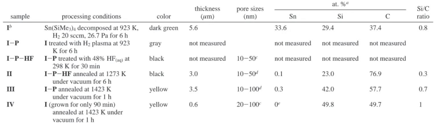
Table 1. Summary of Samples
at. %a
sample processing conditions color
thickness (µm) pore sizes (nm) Sn Si C Si/C ratio Ib Sn(SiMe 3)4decomposed at 923 K, H220 sccm, 26.7 Pa for 6 h dark green 5.6 33.6 29.4 37.4 0.8
I-P I treated with H2plasma at 923 K for 6 h
gray not measured not measured not measured not measured I-P-HF I-P treated with 48% HF(aq)at
298 K for 30 min
black not measured 10-50c not measured not measured not measured
II I-P-HF annealed at 1273 K under vacuum for 6 h
black 3.0 10-50d 0.1 23.0 76.9 0.3
III I-P annealed at 1423 K under vacuum for 1 h
yellow 3.5 10-100d 0.3 42.0 57.7 0.7
IV I (grown for only 90 min) annealed at 1423 K under vacuum for 1 h
yellow 0.6 20-100c 0e 49.8 49.7 1
aAtomic ratios were calculated from EPMA data.bFrom position 4 in the reactor.cEstimated from SEM image.dEstimated from SEM and TEM
images.eBelow detection limit.
Figure 3. (A) SEM, EDX (inset), and (B) XRD pattern of I. I was grown from Sn(SiMe3)4at 923 K, H2flow rate 20 sccm, and 26.7 Pa.
Figure 4. (A) SEM and (B) EDX of I-P-HF, prepared by treating I with H2plasma at 923 K followed by etching in HF(aq)at 298 K.
Figure 5. (A) SEM, (B) EDX, (C) cross-sectional SEM, and (D) TEM and ED (inset) of II, obtained by annealing I-P-HF at 1273 K under vacuum.
shows a slightly curved I-V feature with an overall resistance of 386Ω. Since the value is between the values of common metals and insulators, we propose that the Sn particles are loosely connected in this sample. In Figure 7C, III shows a nonlinear I-V curve. At an applied bias of (5 V, the current passing through the junction between the film and the wafer in III is 0.1-27 mA. The resistivity, estimated from the sheet resistance, of III is 1.03Ω·cm. This is within
the literature values of undoped β-SiC thin films on Si wafers.30,31
To evaluate potential device applications, P-N junction diodes were fabricated from mesoporous β-SiC films IV grown on p-type Si wafers. EPMA showed that IV contained 49.8% Si and 49.7% C, which corresponds to the Si/C atomic ratio of 1. The Sn content was below the EPMA detection limit. I-V curves of the devices constructed from undoped and P-doped IV are shown in Figures 8A and 8B, respec-tively. Even thoughβ-SiC is an intrinsic n-type semiconduc-tor, it is obvious that after the film was doped, the n-β-SiC/ p-Si heterojunction is significantly improved to show a diode-like rectifying behavior.32,33 A SIMS depth profile study showed that C, P, and Sn secondary ion concentrations dropped significantly at a depth of ca. 0.6-0.8 µm. This agrees well with the film thickness observed using SEM, 0.6µm. At the junction, the P atom concentration was ca. 2
× 1017atoms/cm3. We suggest that the diode performance was indeed enhanced by the doping process.
3.5. Reaction Pathway Elucidation. Volatile species generated in the MOCVD process were trapped at 77 K and analyzed by GC-MS. The major components were identified to be HSiMe3, Si2Me6, and [Me2SiCH2]2 (1,1,3,3-tetramethyl-1,3-disilacyclobutane). In addition to these molecules, on-line RGA data suggested that H2, CH4, C2H2, and C2H4, which could not be trapped at 77 K, were also formed in the decomposition process. Since no Sn-containing molecules were detected in the gas-phase byproducts and Sn crystallized into metallic nanoparticles, we propose that the Sn-Si bonds in the precursor Sn(SiMe3)4decomposed extensively during the MOCVD process. Sn(SiMe3)4might loose SiMe3radicals sequentially into metastable Sn(SiMe3)3 and Sn(SiMe3)2 species and finally into metallic Sn.13,34These silyl species,
(30) Gorin, S. N.; Ivanova, L. M. Phys. Status Solidi B 1997, 202, 221. (31) Wijesundara, M. B.; Gao, J. D.; Carraro, C.; Howe, R. T.; Maboudian,
R. J. Cryst. Growth 2003, 258, 18.
(32) Muto, H.; Asano, T.; Wang, R.-P.; Kusumori, T. Appl. Phys. Lett. 2005, 87, 162106.
(33) Furukawa, K.; Vemoto, A.; Shigeta, M.; Suzuki, A.; Nakajima, S. Appl. Phys. Lett. 1986, 45, 1536.
(34) (a) Wro´bel, A. M.; Wickramanayaka, S.; Nakanishi, Y.; Hatanaka, Y.; Pawowski, S.; Olejniczak, W. Diamond Relat. Mater. 1997, 6, 1081. (b) Wro´bel, A. M.; Stanczyk, W. Chem. Mater. 1994, 6, 1766. (c) Wro´bel, A. M.; Wickramanayaka, S.; Nakanishi, Y.; Fukuda, Y.; Hatanaka, Y. Chem. Mater. 1995, 7, 1403. (d) Wro´bel, A. M.; Figure 6. (A) SEM, (B) EDX, (C) cross-sectional SEM, (D)
low-magnification TEM, (E) SAED, and (F) HRTEM from the red-square area in (D) of III, obtained by annealing I-P at 1423 K under vacuum.
Figure 7. I-V characteristics of (A) I, grown from Sn(SiMe3)4at 923 K,
H2flow rate 20 sccm, and 26.7 Pa; (B) I-P annealed at 1073 K, prepared
by treating I with H2plasma at 923 K and annealed at 1073 K; and (C) III,
obtained by annealing I-P at 1423 K under vacuum.
Figure 8. I-V characteristics of (A) IV/p-type Si junction and (B) P doped-IV/p-type Si junction. IV was prepared by annealing I (grown for only 90
including the SiMe3radicals evolved and the silane byprod-ucts observed, probably decompose on the substrate surface to deposit the amorphous SiC1+xlayer. Due to a large size difference between the elements, the thermodynamic solubil-ity of Sn in Si and C is low.35,36 For example, thermal decomposition of alkyltin compounds generated elemental Sn and C.37-39 In this study, the formation of phase-segregated Sn and amorphous SiC1+xis attributed to the same reason. This is in contrast to the solubility of Ge in Si and SiC.40-42After the removal of Sn nanoparticles, the amor-phous SiC1+xlayer was transformed intoβ-SiC by thermal treatments. The formation of separated Si and C phases was not observed.
The experimental processes performed in this study are shown in Scheme 1. Based on the experimental observations, we suggest that the initially deposited thin film I is a composite of sporadic Sn nanoparticles embedded in a preceramic amorphous SiC1+xlayer. Then, upon H2plasma processing at 923 K, I is converted to I-P. In the process, I is etched to form volatile silanes and hydrocarbons and to leave pores and channels inside the films. These defects would allow fluidic Sn nanoparticles embedded in the preceramic amorphous SiC1+xlayer to migrate to the surface easily. The Sn particles would agglomerate into larger ones
to reduce the surface tension by ostwald ripening.43-45Then, the Sn particles could be removed from I-P by dipping it into an HF solution to generate a mesoporous amorphous SiC1+xthin film I-P-HF. After the film was annealed at 1273 K under vacuum to evaporate residual Sn, amorphous SiC1+x (x ) 2.3) II retaining the mesoporous structure is formed. On the other hand, a simple annealing of I-P at 1423 K generates porous β-SiC III by evaporating Sn particles and crystallizing the SiC component in the film.
4. Conclusions
We have demonstrated a new strategy to fabricate meso-porous silicon carbide thin films by growing a precursor film which contains sporadic Sn nanoparticles embedded in amorphous SiC1+x on Si at 923 K by MOCVD from Sn-(SiMe3)4. The unique phase-segregated film structure is attributed to the low solubility of Sn in SiC. The precursor film can be processed further under hydrogen plasma, in HF(aq), and at high temperature to remove Sn from the deposited layer and convert it into a mesoporous SiC thin film on Si. We also demonstrated how to fabricate p-n junction diodes from the mesoporous n-type SiC thin film on p-type Si wafer. We expect that many unique devices may be developed for future applications.
Acknowledgment. We are grateful for the support from the National Science Council and the Ministry of Education of Taiwan, Republic of China.
Supporting Information Available: Photo images, SEM, EDX, TEM, ED, EPMA, XPS, Raman, FT-IR, XRD, GC-MS, and SIMS (PDF). These materials are available free of charge via the Internet at http://pubs.acs.org.
CM0710498
Walkiewicz-Pietrzykowska, A. Chem. Vap. Deposition 1998, 4, 133. (35) Massalski, T. B.; Okamoto, H.; Subramanian, P. R.; Kacprzak, L. Binary Alloy Phase Diagrams, 2nd ed.; ASM International: Materials Park, OH, 1990; Vol. 3, p 3361.
(36) (a) Ahn, H.-J.; Kim, Y.-S.; Park, K.-W.; Seong, T.-Y. Chem. Commum. 2005, 1, 43. (b) Fyhn, M. F.; Chevallier, J.; Larsen, A. N. J. Vac. Sci.
Technol. B 1998, 16, 1777. (c) Min, K. S.; Atwater, H. A. Appl. Phys. Lett. 1998, 72, 1884.
(37) Margitfalvi, J. L.; Kolosova, I.; Ta´las, E.; Go¨bo¨lo¨s, S. Appl. Catal. A 1997, 154, L1.
(38) Kim, I.-S.; Blomgren, G. E.; Kumta, P. N. Electrochem. Solid-State Lett. 2004, 7, A44.
(39) Liu, Y.; Xie, J. Y.; Takeda, Y.; Yang, J. J. Appl. Electrochem. 2002, 32, 687.
(40) (a) Yonenaga, I. J. Cryst. Growth 2005, 275, 91. (b) Bolkhovityanov, Yu. B.; Deryabin, A. S.; Gutakovskii, A. K.; Revenko, M. A.; Sokolov, L. V. J. Cryst. Growth 2005, 280, 309.
(41) Biskupek, J.; Kaiser, U.; Ga¨rtner, K. J. Electron Microsc. 2005, 54, 493.
(42) Chiu, H.-T.; Shie, C.-S.; Chuang, S.-H. J. Mater. Res. 1995, 10, 2257.
(43) (a) Wen, H.-C.; Yang, K.; Ou, K.-L.; Wu, W.-F.; Luo, R.-C.; Chou, C.-P. Microelectron. Eng. 2005, 82, 221. (b) Uh, H. S.; Park, S. S. J. Electrochem. Soc. 2004, 151, H164.
(44) Zhang, J. H.; Feng, T.; Yu, W. D.; Liu, X. H.; Wang, X.; Li, Q. Diamond Relat. Mater. 2004, 13, 24.
(45) (a) Weng, C.-H.; Su, H.-C.; Yang, C.-S.; Shin, K.-Y.; Leou, K.-C.; Tsai, C.-H. Nanotechnology 2006, 17, 5644. (b) Fillot, F.; To¨kei, Zs.; Beyer, G. P. Surf. Sci. 2007, 601, 986.