國 立 交 通 大 學
電子工程學系 電子研究所
博 士 論 文
具高介電常數閘極絕緣層的低溫多晶矽薄膜電晶體之
研究
Investigation on Low-Temperature Polycrystalline-Silicon
Thin-Film Transistor with High-κ Gate Dielectric
研 究 生 :馬 鳴 汶
指導教授 :雷 添 福 博士
趙 天 生 博士
具高介電常數閘極絕緣層的低溫多晶矽薄膜電晶體之
研究
Investigation on Low-Temperature
Polycrystalline-Silicon Thin-Film Transistor with
High-
κ Gate Dielectric
研 究 生:馬鳴汶 Student:Ming-Wen Ma
指導教授:雷添福 博士 Advisor:Dr. Tan-Fu Lei
趙天生 博士 Dr. Tien-Sheng Chao
國立交通大學
電子工程學系 電子研究所
博士論文
A Dissertation
Submitted to Department of Electronics Engineering
and Institute of Electronics
College of Electrical and Computer Engineering
National Chiao Tung University
In Partial Fulfillment of the Requirements
For the Degree of
Doctor of Philosophy
in
Electronics Engineering
June 2008
HsinChu, Taiwan, Republic of China
具高介電常數閘極絕緣層的低溫多晶矽薄膜電晶體之
研究
學生:馬 鳴 汶 指導教授:雷 添 福 博士
趙 天 生 博士
國立交通大學
電子工程學系 電子研究所博士班
摘要
在本論文中,我們詳細地探討高性能之具二氧化鉿(HfO2)的低溫薄膜電 晶體之元件特性。本論文首先特別針二氧化鉿(HfO2)與多晶矽薄膜之間所產 生的介面層(interfacial layer),對於低溫多晶矽薄膜電晶體的特性影響上作了 仔細的分析,特別是二氧化鉿的介面層對於 N 型與 P 型通道之低溫薄膜電晶體 的影響。此外,為了更進一步研究與加強二氧化鉿之低溫薄膜電晶體的特性,氧 氣電漿表面處理也被使用來改善多晶矽通道的表面品質與鈍化缺陷,可增加載子 遷移率與降低表面粗糙散射(surface roughness scattering)。另外,氮氣和氨氣 電漿表面處理可個別地明顯地增加二氧化鉿之低溫薄膜電晶體的載子遷移率約 74.4 和 108.5 個百分比。而且,氮氣和氨氣電漿表面處理也可降低表面粗糙散射 來增加在高的閘極偏壓下之載子遷移率,可個別地提升二氧化鉿之低溫薄膜電晶 體的驅動電流約 217 和 219.6 個百分比。 另外,我們也詳細地探討高性能之具二氧化鉿(HfO2)的低溫薄膜電晶體 之可靠度機制。施加多種偏壓與溫度的應力條件以用於釐清陷阱密度能態(trapdensity states)的分佈與機制。藉由施予閘極正偏壓應力(PBS)與閘極正偏壓 高溫應力(PBTI)在二氧化鉿之低溫薄膜電晶體上,可以觀察到等效介面層之 深層陷井能態的產生、多晶矽晶界之淺層陷井能態的產生、以及二氧化鉿之電子 捕捉。而閘極負偏壓應力(NBS)與閘極負偏壓高溫應力(NBTI)施予在二氧 化鉿之低溫薄膜電晶體可以觀察到等效介面層之深層與淺層陷井能態的產生。 除了電漿表面處理之外,氟與氮離子佈植法配以固態低溫活化法也可達到高 性能的二氧化鉿之低溫薄膜電晶體。對於氟離子佈植法而言,二次離子質譜儀的 分析展現了與過往研究中不同的氟離子分佈,造成約有百分之 25 的晶界缺陷陷 阱被氟離子鈍化且導致漏電電流降低約十倍。另外,熱載子效應對於臨界電壓不 穩定度也有了改善。具二氧化鉿之低溫多晶矽薄膜電晶體配以氟離子佈植法可達 到低臨界電壓約 1.32 V、優異的次臨界斜率約 0.141 V/decade、和高開關電流比 1.98 x 10⁷。然而對於氮離子佈植法而言,二次離子質譜儀的分析展現了氮離子在 佈植後的退火過程中,將會聚集在多晶矽通道與絕緣層的介面處,對於 N 型低 溫多晶矽薄膜電晶體而言,將會造成百分之 54.9 的驅動電流增加量,然而對於 P 型低溫多晶矽薄膜電晶體而言,將會造成百分之 16.7 的驅動電流增加量。因此, 對具二氧化鉿之低溫多晶矽薄膜電晶體配以氮離子佈植法可達到低臨界電壓:N 型約為 1.05 V,P 型約為-0.8 V、優異的次臨界斜率:N 型為 0.213 V/decade,P 型為 0.123 V/decade、以及較高的載子遷移率:N 型為 37.80 cm2/V-s,P 型為 64.14 cm2/V-s。這些具二氧化鉿之低溫多晶矽薄膜電晶體的改善,均歸功於較高的閘 極電容密度以及氟與氮離子對於多晶矽薄膜缺陷的鈍化。 最後,此論文也展示了利用金屬側向誘發結晶法配以氮化鉭/二氧化鉿 (TaN/HfO2)結構之 P 型通道低溫薄膜電晶體。低臨界電壓約 0.095 V、優異次 臨界斜率約 83 mV/decade、和超高載子遷移率 240 cm2 /V-s 可被實現而不需要任 何的缺陷鈍化處理。此明顯的電性改善主要是來自於利用金屬側向誘發結晶法所 產生的通道薄膜以及非常高的閘極電容密度。
Investigation on Low-Temperature
Polycrystalline-Silicon Thin-Film Transistor with
High-
κ Gate Dielectric
Student: Ming-Wen Ma Advisor: Dr. Tan-Fu Lei
Dr. Tien-Sheng Chao
Department of Electronics Engineering &
Institute of Electronics
National Chiao Tung University
Abstract
In this dissertation, the impacts of HfO2 interfacial layer on n- and p-channel LTPS-TFTs are specified. In order to enhance the characteristics of HfO2 LTPS-TFT further, oxygen plasma surface treatment is employed to improve the interface quality and passivate the defects of channel grain boundaries, resulting in increasing the carrier mobility and reducing the surface roughness scattering. Moreover, significant field effect mobility μFE improvement ~ 74.4 % and 108.5 % are observed for LTPS-TFTs with HfO2 gate dielectric after N2 and NH3 plasma surface treatments, respectively. In addition, the N2 and NH3 plasma surface treatments can also reduce the surface roughness scattering to enhance the field effect mobility μFE at high gate bias voltage VG, resulting in 217.0 % and 219.6 % improvement in driving current,
respectively.
In addition, a comprehensive study of the reliability mechanisms of the high performance low-temperature poly-Si thin-film transistor (LTPS-TFT) with HfO2 gate dielectric is also demonstrated. Various bias and temperature stress conditions, which correspond to positive bias stress (PBS), positive bias temperature instability (PBTI), negative bias stress (NBS), negative bias temperature stability (NBTI), and hot carrier stress, are used to differentiate the distribution and mechanism of trap density states. The generation of deep trap states of the effective interfacial layer, tail trap states of poly-Si grain boundaries, and electrons trapping of the HfO2 gate dielectric are observed for the PBS and PBTI of the HfO2 LTPS-TFT. In addition, both the deep and tail trap states of the effective interfacial layer are generated under NBS and NBTI of the HfO2 LTPS-TFT. Moreover,
In addition to the plasma surface treatment, fluorine and nitrogen ion implantation with low temperature solid-phase crystallized activation scheme is used to obtain a high performance HfO2 LTPS-TFT. For fluorine ion implantation of LTPS-TFT, the SIMS analysis shows a different fluorine profile compared to that annealed at high temperature. About one order current reduction of Imin is achieved due to 25 % grain-boundary traps are passivated by fluorine implantation. In addition, the threshold voltage instability of hot carrier stress is also improved with the introduction of fluorine. The LTPS-TFT with HfO2 gate dielectric and fluorine pre-implantation can simultaneously achieve low VTH ~ 1.32 V, excellent S.S. ~ 0.141 V/decade, and high Ion/Imin current ratio ~ 1.98 x 10⁷. For nitrogen ion implantation of LTPS-TFT, the SIMS analysis shows the nitrogen atoms would pile up near the surface of poly-Si channel film after SPC process. For n-channel LTPS-TFT, a ~ 54.9 % driving current IDsat improvement is found. For p-channel LTPS-TFT, a ~ 16.7 % driving current IDsat improvement is found. Finally, a high performance CMOS
LTPS-TFTs with threshold voltage VTHn ~ 1.05 V, VTHp ~ –0.8 V, subthreshold swing S.S.n ~ 0.213 V/dec., S.S.p ~ 0.123 V/dec., field effect carrier mobility μnFE ~ 37.80 cm2/V-s and μpFE ~ 64.14 cm2/V-s are derived. The performance improvements of LTPS-TFTs after NII treatment are due to the defect passivation near the surface channel by nitrogen atoms.
Finally, high-performance low-temperature poly-Si (LTPS) p-channel thin-film transistor (TFT) with metal-induced lateral crystallization (MILC) channel layer and TaN/HfO2 gate stack is demonstrated. Devices of low threshold voltage VTH ~ 0.095 V, excellent subthreshold swing S.S. ~ 83 mV/dec., and high field effect mobility μFE ~ 240 cm2/V-s are achieved without any defect passivation methods. These significant improvements are due to the MILC channel film and the very high gate capacitance density provided by HfO2 gate dielectric with the effective oxide thickness (EOT) of 5.12 nm.
誌謝
在此我要感謝我的指導老師雷添福教授與趙天生教授,在我處於人生的徘徊 進退中,給予我最大的幫助與鼓勵。還有在這三年中所給我熱心的指導與教誨, 使我在學術研究及待人處事上獲益匪淺,僅在此表達由衷的感謝之意。此外還要 感謝在我進入交大電子所博士班時給我鼓勵的桂正媚教授、顏順通教授、徐琅教 授、以及謝太炯教授,由於你們的支持與鼓勵,才能使我在內心孤立無援時注入 熱情,得以在求學的路上繼續邁進,在此致上滿心的感謝。若沒有各位教授們的 扶持,相信學生今天難以拿到博士學位。另外我特別要感謝是胡振國教授與管傑 雄教授,在我就讀台大期間進退失據時,能對學生伸出援手,真是感激不盡。 另外,我還要感謝在這段過程的郭柏儀學長、陳建豪學長、羅文政學長、謝 明山學長、游信強學長、楊紹明學長、林育賢學長、王獻德學長們的支持與指教。 除此之外,我還要感謝實驗室的同學與學弟妹們:吳偉成、陳志仰、蘇俊榮、呂 宗宜、高興、宗諭、美君、德鑫、阿壘、姸心、俊祥、武欽、猴子、彥學、佩珊、 宗育、智盟、冠迪、翊鴻、廖博、威良,有了你們,才讓我的研究生活充滿了歡 樂與色彩,使我有動力繼續努力研究下去,感謝大家的支持與鼓勵,謝謝你們。 在此也要感謝奈米中心的技術員們的幫忙,葉雙得先生、胡進章先生、陳明 麗小姐、林聖欽先生、范秀蘭小姐、黃月美小姐、徐秀鑾小姐……等。另外還要 感謝 NDL 的技術員們的幫忙,趙子綾小姐、林婉貞小姐、范庭瑋小姐、陳琇芝 小姐、鄭旭君先生、陳世哲先生……等。感謝各位們的幫忙,讓這本博士論文能 順利誕生,謝謝各位對於我實驗上的照顧與幫忙,由衷地感謝。 此外,也感謝在博士班三年間陪伴我走過來的宜真,總是給我正面積極的加 油與照顧,也謝謝她的支持與諒解,謝謝妳。 最後,我要對我的父母馬瑞生先生、詹美玉女士以及家人們獻上最深的謝意 與祝福,由於您們的栽培、支持與鼓勵,我才能有今日的表現。Contents
Abstract (Chinese)………
iAbstract (English)………
iiiAcknowledgement………
viContents………
viiTable Captions………..………….…….
xiFigure Captions………....
xiiiChapter 1 Introduction of Low-Temperature Polycrystalline-Silicon
Thin-Film Transistor Introduction
1.1 Background of Silicon Channel Thin-Film Transistors………..11.2 Electrical Characteristics of Polycrystalline-Silicon………..2
1.2.1 Seto’s model………...3
1.2.2 Baccarani’s model………..7
1.2.3 J. Levinson’s current equation of polycrystalline-silicon thin-film transistor………10
1.3 Dissertation Organization………13
Chapter 2 Investigation of HfO2/Poly-Si Interfacial Layer on
CMOS Low-Temperature Polycrystalline-Silicon
Thin-Film Transistor, Including O2, N2, NH3 Plasma
Surface Treatment
2.1 Impacts of HfO2/Poly-Si Interfacial Layer on CMOS Low-Temperature Polycrystalline-Silicon Thin-Film Transistor with HfO2 Gate Dielectric……….192.1.2 Fabrication Process………..21 2.1.3 Discussion of Impacts of Interfacial Layer on LTPS-TFT with HfO2 Gate
Dielectric………..22 2.1.4 Summary………..25 2.2 Characteristics of HfO2/Poly-Si Interfacial Layer with N2 and NH3 Plasma
Surface Treatment on Low-Temperature Polycrystalline-Silicon Thin-Film Transistor with HfO2 Gate Dielectric………26 2.2.1 Introduction………..26 2.2.2 Discussion of Impacts of N2 and NH3 Plasma Surface Treatment on
Low-Temperature Polycrystalline-Silicon Thin-Film Transistor with HfO2 Gate Dielectric………..27 2.2.3 Summary………..29
Chapter 3 The Adoption of HfO2 Gate Dielectric for the
Low-Temperature Polycrystalline-Silicon Thin-Film
Transistor: Performance and Reliability Mechanism
3.1 Introduction of Low-Temperature Polycrystalline-Silicon Thin-Film Transistor with HfO2 Gate Dielectric……….48 3.2 Fabrication Process………...49 3.3 High-Performance LTPS-TFT with HfO2 Gate Dielectric………50 3.4 Reliability Mechanisms of High-Performance LTPS-TFT with HfO2 Gate
Dielectric………...51 3.5 Summary………...57
Chapter 4 Impacts of Fluorine and Nitrogen Ion Implantation on
Low-Temperature Polycrystalline-Silicon Thin-Film
Transistor with HfO2 Gate Dielectric
4.1 The fluorine ion implantation before solid phase crystallization………….…….74
4.1.1 Introduction………..……74
4.1.2 Fabrication Process……….………...75
4.1.3 Discussion………….………...76
4.1.4 Summary………..80
4.2 The nitrogen ion implantation after solid phase crystallization………...….80
4.2.1 Introduction………..80
4.2.2 Fabrication Process……….………...80
4.2.3 Discussion………….……….…..81
4.2.4 Summary………...83
Chapter 5 High Performance Metal-Induced Lateral Crystallized
Polycrystalline Silicon P-Channel Thin-Film Transistor
with TaN/HfO2 Gate Stack Structure
5.1 Introduction……….1025.2 Fabrication Process……….103
5.3 Discussion………...104
5.4 Summary……….106
Chapter 6 Conclusions and Recommendations for Future Research
6.1 Conclusions……….111Reference
………....115Publication List
………....131Table Captions
Chapter 2
Table 2-I. Important parameters of CMOS HfO2 LTPS-TFTs without oxygen plasma surface treatment and conventional CMOS LTPS-TFTs with SiO2 gate dielectric………..30 Table 2-II. Important parameters of CMOS HfO2 LTPS-TFTs with and without
oxygen plasma surface treatment………31 Table 2-III. Important device parameters of LTPS-TFT with HfO2 gate dielectric
after N2 and NH3 plasma surface treatment for 5-min and 15-min, respectively………..32
Chapter 3
Table 3-I. Device parameter comparison of the HfO2 gate dielectric TFTs. Other gate dielectric TFTs are also listed for comparison……….59 Table 3-II. Degradation of experimental electrical characteristics and corresponding possible degradation mechanisms………...60
Chapter 4
Table 4-I. The important parameters of the HfO2 LTPS-TFT without and with fluorine pre-implantation………84 Table 4-II. The important parameters of the n-channel LTPS-TFT with HfO2 gate
dielectric and NII treatment, which conventional LTPS-TFT with thick SiO2 gate dielectric and other’s work are included………85 Table 4-III. The important parameters of the p-channel LTPS-TFT with HfO2 gate
SiO2 gate dielectric and other’s work are included……….86
Chapter 5
Table 5-I. The important parameters of the TaN/HfO2 gate stack structure LTPS-TFT with MILC channel film. Others’ works are also listed for compare…...107
Figure Captions
Chapter 1
Fig. 1-1. The cross-section view of polycrystalline-silicon thin-film transistor…….15 Fig. 1-2. Sketch of the band diagram in polycrystalline-silicon thin-film…………..16 Fig. 1-3. Barrier height versus impurity concentration………...17 Fig. 1-4. Barrier height versus impurity concentration………...18
Chapter 2
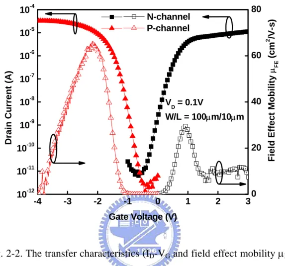
Fig. 2-1. The cross-sectional view of CMOS LTPS-TFTs with HfO2 gate dielectric and oxygen plasma surface treatment………..33 Fig. 2-2. The transfer characteristics (ID-VG and field effect mobility μFE) of CMOS
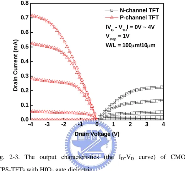
HfO2 LTPS-TFTs without oxygen plasma surface treatment………...34 Fig. 2-3. The output characteristics (the ID-VD curve) of CMOS LTPS-TFTs with
HfO2 gate dielectric………..35 Fig. 2-4. The transfer characteristics (ID-VG and field effect mobility μFE) of
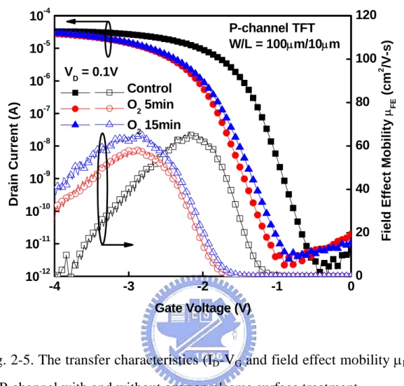
N-channel with and without oxygen plasma surface treatment…………...36 Fig. 2-5. The transfer characteristics (ID-VG and field effect mobility μFE) of
P-channel with and without oxygen plasma surface treatment………37 Fig. 2-6. The ID-VD curve of N-channel HfO2 LTPS-TFTs with and without oxygen
plasma surface treatment………..38 Fig. 2-7. The ID-VD curve of P-channel HfO2 LTPS-TFTs with and without oxygen
plasma surface treatment………..39 Fig. 2-8. The normalized field effect mobility μEF of N-channel HfO2
Fig. 2-9. The normalized field effect mobility μEF of P-channel HfO2 LTPS-TFTs...41 Fig. 2-10. The transfer characteristics (ID-VG and transconductance Gm) of LTPS-TFT
with HfO2 gate dielectric after N2 and NH3 plasma surface treatment for 5-min………42 Fig. 2-11. The transfer characteristics (ID-VG and transconductance Gm) of LTPS-TFT
with HfO2 gate dielectric after N2 and NH3 plasma surface treatment for 15-min………..43 Fig. 2-12. The output characteristics (ID-VD) curve of LTPS-TFT with HfO2 gate
dielectric after N2 and NH3 plasma surface treatment for 5-min………….44 Fig. 2-13. The output characteristics (ID-VD) curve of LTPS-TFT with HfO2 gate
dielectric after N2 and NH3 plasma surface treatment for 15-min………...45 Fig. 2-14. The normalized field effect mobility μEF of LTPS-TFT with HfO2 gate
dielectric after N2 and NH3 plasma surface treatment for 5-min………….46 Fig. 2-15. The normalized field effect mobility μEF of LTPS-TFT with HfO2 gate
dielectric after N2 and NH3 plasma surface treatment for 15-min………...47
Chapter 3
Fig. 3-1. The cross-section structure of Al/HfO2/poly-Si n-channel LTPS-TFT with different VG and VD stress bias for 1000-s. The locations of stress damage are also indicated………..61 Fig. 3-2. The ID-VG and transconductance Gm characteristics of the HfO2 LTPS-TFT
with W/L = 100 μm/10 μm………...62 Fig. 3-3. The ID-VG characteristics of the HfO2 LTPS-TFT before and after different gate bias stresses with fixed VD = 0V for 1000-s at 25°C………63 Fig. 3-4. The transconductance Gm and subthreshold swing S.S. of the HfO2
LTPS-TFT before and after different gate bias stresses with fixed VD = 0V for 1000-s at 25°C………64 Fig. 3-5. The gate leakage current of the HfO2 LTPS-TFT before and after different
gate bias stresses with fixed VD = 0V for 1000-s at 25°C………65 Fig. 3-6. The ID-VG and transconductance Gm characteristics of the HfO2 LTPS-TFT
before and after different gate bias stresses with fixed VD = 0V for 1000-s at 125°C………66 Fig. 3-7. The transconductance Gm and subthreshold swing S.S. characteristics of the HfO2 LTPS-TFT before and after different gate bias stresses with fixed VD = 0V for 1000-s at 125°C……….67 Fig. 3-8. The gate leakage current of the HfO2 LTPS-TFT before and after different
gate bias stresses with fixed VD = 0V for 1000-s at 125°C………..68 Fig. 3-9. Energy band diagram of the HfO2 LTPS-TFT under (a) PBTI and (b) NBTI stress……….69 Fig. 3-10. The transconductance Gm and subthreshold swing S.S. characteristics of the
HfO2 LTPS-TFT before and after different gate bias stresses with fixed VD = 0V and VD = 5V for 1000-s at 25°C………..70 Fig. 3-11. The ID-VG and transconductance Gm characteristics of the HfO2 LTPS-TFT before and after different gate bias stresses with fixed VD = 5V for 1000-s at 125°C………71 Fig. 3-12. The cross-section structure of Al/HfO2/poly-Si n-channel LTPS-TFT with
drain bias stress for 1000-s. The magnitudes of vertical electric field are also indicated………72 Fig. 3-13. The ID-VG characteristics of the HfO2 LTPS-TFT before and after different drain bias stresses with fixed VG – VTH = 5V for 1000-s at 125°C………..73
Chapter 4
Fig. 4-1. The cross-sectional transmission electron microscopy (TEM) micrograph of the HfO2 gate dielectric TFT structure……….87 Fig. 4-2. The SIMS analysis of the HfO2 LTPS-TFT with fluorine
pre-implantation………...88 Fig. 4-3. Transfer characteristics (ID-VG and Gm) of the HfO2 LTPS-TFT at VD = 0.1
V without and with fluorine pre-implantation before and after hot carrier stress VG – VTH = VD = 5V for 1000 seconds………...89 Fig. 4-4. The plots of ln [IDS/(VGS - VFB)] versus 1/(VGS - VFB)2 curves at VDS = 1 V and high VGS……….90 Fig. 4-5. The threshold voltage shift ΔVT of TaN/HfO2 LTPS-TFTs with and without fluorine implantation after 1000-s hot carrier stress VG – VTH = 5V, VD = 10V………...91 Fig. 4-6. The gate leakage current of TaN/HfO2 LTPS-TFTs with and without
fluorine implantation during the hot carrier stress VG – VTH = 5V, VD = 10V………...92 Fig. 4-7. The transconductance Gm degradation of TaN/HfO2 LTPS-TFTs with and
without fluorine implantation during 1000-s hot carrier stress VG – VTH = 5V, VD = 10V………93 Fig. 4-8. The driving current of TaN/HfO2 LTPS-TFTs with and without fluorine
implantation during 1000-s hot carrier stress VG – VTH = 5V, VD = 10V………...94 Fig. 4-9. The transfer characteristics (ID-VG and Gm) of n-channel LTPS-TFT with
HfO2 gate dielectric and NII treatment……….95 Fig. 4-10. The transfer characteristics (ID-VG and Gm) of p-channel LTPS-TFT with HfO2 gate dielectric and NII treatment………96
Fig. 4-11. The output characteristics (ID-VD) of n-channel LTPS-TFT with HfO2 gate dielectric and NII treatment………..97 Fig. 4-12. The output characteristics (ID-VD) of p-channel LTPS-TFT with HfO2 gate dielectric and NII treatment………..98 Fig. 4-13. The secondary ion mass spectrometer (SIMS) of poly-Si channel film after NII treatment………99 Fig. 4-14. The plot of ln[ID/(VG – VFB)] versus 1/(VG – VFB)2 curves at VD = 0.1 V and
high VG of n-channel LTPS-TFT………100 Fig. 4-15. The plot of ln[ID/(VG – VFB)] versus 1/(VG – VFB)2 curves at VD = 0.1 V and high VG of p-channel LTPS-TFT………101
Chapter 5
Fig. 5-1. The cross-section view and process flow of the TaN/HfO2 gate stack structure LTPS-TFT with MILC channel film………...108 Fig. 5-2. The transfer characteristics (ID-VG and transconductance Gm) of LTPS-TFT
with TaN/HfO2 gate stack structure and MILC polycrystalline silicon channel film. The inserted figure is the C-V curve of TaN/HfO2 capacitor……….109 Fig. 5-3. The output characteristic ID-VD of MILC LTPS-TFT with TaN/HfO2 gate
Chapter 1
Introduction of Low-Temperature Polycrystalline-Silicon
Thin-Film Transistor
1.1 Background of Silicon Channel Thin-Film Transistors
Silicon channel thin-film transistors (TFTs) have been widely investigated for the application of pixel driving device of active matrix liquid crystal display (AMLCD) [1.1]-[1.3]. The liquid crystal of LCD can show different polarization to make the incident white light reveal different colors. In order to control the polarization of liquid crystal, a switch device of liquid crystal is required to make the liquid crystal act as a display monitor. Therefore, the switch devices must be embedded in the glass panel to control the polarization of liquid crystal. The fabrication processes of switch devices are limited by the melting point of glass panel because the fabrication of switch devices is not separating from glass panel. Amorphous-silicon channel TFTs are generally chosen to be the switch device of AMLCD in LCD industry. However, the driving current of amorphous-Si TFT is very low because the amorphous-silicon film is less conductive, which is corresponding to very low field effect carrier mobility μEF about several cm2/V-s. With the development of large-size display panel, high driving current of switch device of liquid crystal is urgently needed to drive amount of pixels and enhance the respond time of liquid crystal. Low-temperature polycrystalline-silicon (LTPS) thin-film transistors have been studied instead of amorphous silicon [1.4]-[1.8]. This is because the field effect carrier mobility μEF in polycrystalline silicon is significantly higher (by one ~ two orders of magnitude) than that in amorphous silicon [1.9], so that the switch devices of liquid crystal with
reasonably high drive currents can be achieved in polycrystalline silicon.
In addition to the switch device of liquid crystal pixel, the functional electronic circuits of LCD are wanted to be integrated on the panel, which is named system-on-panel (SOP). Recently, the topic of SOP is attracting much attention to realize [1.6]. In order to achieve high functional integrated circuits, high-performance TFTs with high driving current, low gate leakage current, low threshold voltage VTH and low subthreshold swing S.S. are required urgently for high-speed display driving circuits.
Beside the application of display industry, the device structure of silicon-channel TFT is the same as the silicon-on-insulator (SOI) device of microelectronics. The difference of TFT and SOI device is the crystal phase of silicon channel film that amorphous- and polycrystalline-silicon channel are usually referred to TFT and the single-crystalline silicon channel film is referred to SOI device. SOI device exhibits ultra-high performance characteristics to be applied in very large scale integrated circuits (VLSI) technology. However, the cost of SOI device is very expensive. In recent years, TFTs device have been studied for the application of Dynamic Random Access Memory (DRAM) and Static Random Access Memory (SRAM) in the back-end fabrication process of VLSI technology [1.10][1.11]. The three-dimension integration of integrated circuits technology has been paid much attention to realize because the chip area of integrated circuits can be reduced and the cost of TFT device is much cheaper than single-crystalline MOSFETs and SOI devices. Therefore, the idea of system-on-panel and three-dimension integration would be a novel development of semiconductor industry.
1.2 Electrical Characteristics of Polycrystalline-Silicon
The performance of TFT is limited by the electrical characteristics of polycrystalline-silicon channel film. Therefore, the studies of electrical characteristics of polycrystalline-silicon are very important.
1.2.1 Seto’s model
John Y. W. Seto proposed a model to describe the electrical properties of polycrystalline silicon thin-film in 1975 [1.12]. Seto’s model has some assumptions as shown below:
Assumption:
1. Polycrystalline-silicon is composed of identical crystallites having a grain size of L cm.
2. There is only one type of impurity atom present, the impurity atoms are totally ionized, and uniformly distributed with a concentration of N cm-3.
3. The single-crystalline silicon energy band structure is assumed to be applicable inside the crystallites.
4. The grain boundary is of negligible thickness compared to L and contains Qt cm-2 of traps located at energy Et with respect to the intrinsic Fermi-level.
5. The traps are assumed to be initially neutral and become charged by trapping a carrier.
6. Abrupt depletion approximation.
I. Potential barrier derivation
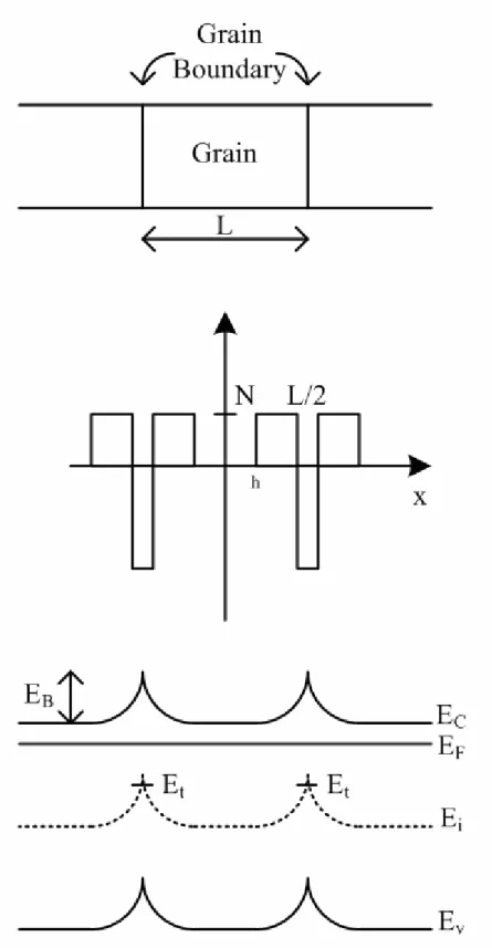
As shown in Fig. 1-2 that indicates the grain size L, dopant concentration N, and the depletion width 2(L/2 – h). From Poisson’s equation:
ε qN dx V d − = 2 2 , h x L 2 1 < < (1)
Æ qN x C1 dx dV = − + ε (2) and =0 =h x dx dV Æ ε qNh C1 = Æ qN (h x) dx dV = − ε Æ 2 0 ) ( ( ) 2 x h V qN Vx = − + ε , h x 2L 1 < < (3)
V0 is the potential of the conduction band edge at the corner of the crystallite. EFi is taken to be at zero energy
a. for LN <Qt Æ h=0 Æ 0 2 ) ( 2 x V qN Vx = + ε , x 2L 1 < (4) so that the potential barrier
ε 8 2 ) 0 ( ) 2 / ( N qL V V VB = L − = (5)
We define the average carrier concentration of polycrystalline-silicon thin-film is Pa and the Boltzmann statistics P(x) is valid,
} ] [ exp{ ( ) ) ( KT E qV N Px = c − x − F (6) ] ) 2 ( 2 [ ) exp( ) 2 ( 1 /2 1/2 1/2 2 / ( ) KT N qL erf KT E E N KT Lq n dx P L P L i B F L x a ε ε π + = =
∫
− (7) B B qV E = , ) 2 exp( KT E N ni = c − g ,According to the number of carriers trapped to the total number of trapping states which are occupied, we can obtain
] exp[ 2 1 KT E E Q LN F t t − + = Æ ) 2 1 ln( − − = LN Q KT E E t t F (8),
Therefore, we can derive the Pa if N, L, Qt and Et are given. b. for LN >Qt Æ h>0
Æ N qQt B ε 8 V 2 = (9)
From the results of equations (5) and (9), we can derive the relation between the potential barrier VB and the doping concentration N of the polycrystalline-silicon thin-film as shown in Fig. 1-3. When the doping concentration of the polycrystalline-silicon N is less than Qt/L, the VB would be higher if the N increased, resulting in the less conductive of polycrystalline-silicon thin-film. When N is higher than Qt/L, the VB would be reduced if the N increased, resulting in the more conductive of polycrystalline-silicon thin-film.
In the non-depletion region:
] ) ( exp[ KT E E N P c F c b − − =
Æ The average carrier concentration Pa:
] ) 2 1 ( 2 [ ) 2 ( 1 ) 1 {( 1 /2 1/2 1/2 2 / ( ) KTN qQ erf N KT Lq LN Q P dx P L P t t b L L x a ε ε π + − = =
∫
− (10)II. Current transport derivation
The resistance of polycrystalline-silicon thin-film can be divided into two parts: grain boundary region and bulk of crystallite, and dominated by the grain boundary region. The current transport mechanisms of polycrystalline-silicon thin-film are thermionic emission and tunneling current. When the carrier energy is higher than the barrier height EB, thermionic emission dominates. On the contrary hand, tunneling current dominates the conduction current when the carrier energy is higher than the barrier height EB. In addition, if the barrier height EB is narrow and high, tunneling current would dominate the conduction current. In polycrystalline-silicon thin-film, the potential is highest when the barrier width is the widest. For highly doped polycrystalline-silicon, potential barrier EB is very small and the tunneling current can
be neglected. From the thermionic emission current density equation Jth: ] 1 ) )[exp( exp( ) 2 ( * 1/2 − − = KT qV KT qV m KT qP J B a a th π (11)
Jth: thermionic emission current Va: applied voltage
By neglecting collisions within the depletion region and the carrier concentration in the crystallite was assumed to be independent of the current flow, so that it is applicable only if the number of carriers which take part in the current transport is small compared to the total number of carriers in the crystallite. This condition restricts the VB > KT. For qVa << KT, a B a th V KT qV KT m P q J ) exp( ) 2 1 ( * 1/2 2 − = π (12) Æ ) exp( ) 2 1 ( * 1/2 2 KT qV KT m P Lq a B − = π σ Æ )] 2 ( 1 exp[ Eg EF KT − − ∝ σ , if LN < Qt ) exp( 2 / 1 KT E T − B ∝ − σ , if LN > Qt In addition, σ =qnμ Æ ) exp( ) 2 1 ( * 1/2 KT E KT m Lq B eff − = π μ (13)
When EB reach maximum, the minimum μeff is obtained. Therefore, the μeff is a function of doping concentration.
Summary of Seto’s model
Physical parameters of model are grain size L, trap charge density Qt, and trap energy level Et.
Qt: N qQ V t B ε 8 2 = (14) ) exp( ) 2 1 ( * 1/2 KT E KT m Lq B eff − = π μ Æ KT E KT m Lq B eff = − ln(2 )− 2 1 ) ln( lnμ π * (15)
From the curve of equation (15), EB can be extracted by the slope of ln(μeff)–1/KT plot. Finally, Qt can be derived.
Et: From equations (7) and (8), Et can be extracted.
1.2.2 Baccarani’s model
After John Y. W. Seto proposed a model to describe the electrical properties of polycrystalline silicon thin-film in 1975 [1.13], G. Baccarani modified Seto’s model in 1978 to propose a modified grain-boundary trapping model as follows:
Modifying the equation (11) by replacing Pa with Na:
a B a th V KT qV KT m N q J ) exp( ) 2 1 ( * 1/2 2 − = π (16) 0 ] ) 2 ( exp[ n KT E E N N F g c a = − − = (17) Æ B F a g c c th V KT E E E KT v N q J exp( 2 ) 2 − + − = (18), *)1/2 2 ( m KT vc π = Æ ) exp( ] ) 2 ( exp[ 0 2 2 KT E KT v Ln q KT E E E KT v LN q B c F B g c c − = − + − = σ (19)
The energy levels are referred to the intrinsic Fermi-level at the neutral region.
G. Baccarani assumed that the grain boundary traps consisted of Qt acceptor states with energy Et referred to the intrinsic Fermi-level at the interface.
Æ ) exp( 2 1 1 ) 2 ( 2 KT E E E Q h L N F B t t D + − + = − (20) ε 2 ) 2 ( 2 2 D B N h L q E − = (21)
ND: doping concentration of polycrystalline-silicon thin-film ND*: charge density trapped by the grain boundaries
A. When ND = ND* Æ h=0 Æ )] 8 ( 1 exp[ 2 1 1 2 2 * 2 2 * ε D F t t D N L q E E KT N L N + − + = Æ * = 82 2{ − + ln[2( * )−1]} L N N KT E E L q N D t t F D ε (22) For small Nt and L Æ
1 * ∝ L−
ND .
For large Nt and L Æ
2 * ∝ L− ND . B. When ND <ND* ε 8 2 2 D B N L q E = , KT E E E N L N F B t t D ) ( exp 2 1 1+ + − = (23) Æ = + − ln[2( −1)] D t B t F LN N KT E E E (24)
In addition, from equation (19),
) exp( ) ( 2 ] ) 2 ( exp[ 2 2 KT E LN N KT v N LN q KT E E E KT v LN q a D t c D c F B g c c − − = − + − = σ (25)
t g a E E E = − 2 (26) C. When ND > ND* ) exp( 2 1 1 ) 2 ( 2 KT E E E N h L N F B t t D + − + = − (27) and ε 2 ) 2 ( 2 2 D B N h L q E − = Æ D B N q E L h 22 2 ε − = (28) Æ ) exp( 2 1 1 2 2 2 KT E E E N N q E N F B t t D B D + − + = ε Æ 1]} 8 [ 2 ln{ − + − = B D t t F B E N qN KT E E E ε (29)
From equation (29), EB would linearly increase with ND as ND < ND*. When ND > ND*, there are two different situations as follows:
1. when EF −Et −EB >>KT Æ ND L − )h ≅ Nt 2 ( 2 Æ D B t N q E N = 2 8ε Æ D D t B N N N q E 1 8 2 2 ∝ ≅ ε (30) 2. when Et +EB −EB >>KT Æ ] ) 2 ( exp[ 0 KT E E N n N F g c D − − = ≈ Æ ) exp( 2 2 ] ) 2 ( exp[ 2 ) 2 ( 2 2 KT E E E N N q E KT E E N h L N F B t t D B F g c D = + − − − = − ε
Æ ] ) 2 ( ln[ 2 1/2 2 / 1 B c t D t g B E N N qN KT E E E ε + − = (31)
Finally, a modified grain-boundary trapping model is derived and the relation between EB and ND can be plotted in Fig. 1-4.
1.2.3 J. Levinson’s current equation of polycrystalline-silicon
thin-film transistor
After John Y. W. Seto and G. Baccarani proposed the physics of polycrystalline-silicon in 1975 and 1978, respectively, J. Levinson proposed the basic current equation of polycrystalline-silicon thin-film transistor at small drain bias based on the Seto and Baccarani’s model in 1982 [1.14].
According thermionic emission equation:
When qVd <<KT, Vd is the voltage drop of a poly-grain
) exp( ) ( 0 2 KT E V KT v n q J B d c th − = (32) 2 / 1 *) 2 ( m KT vc π =
If the number of grain regions is N and the drain voltage is VD Æ Vd = VD/N, For ND < ND* as shown in equation (19)
] ) 2 ( exp[ 2 KT E E E KT v LN q B F g c c − + − = σ , ε 8 2 2 D B N L q E =
For ND >ND* as shown in equation (19)
) exp( 0 2 KT E KT v Ln q c − B = σ Æ 0 0exp( ) KT E qn − B = μ σ (33) KT qLvc = 0 μ (34)
whenEF −Et −EB >>KT Æ D t B N N q E ε 8 2 2 ≅
For the completed description of mobility, the carrier scattering would also occurred at the grain boundaries except the effect of potential barrier. Therefore, the mobility relation should be modified as:
s b μ μ μ 1 1 1 0 + = (35) μ0: effect of the potential barrier
μs: scattering at grain boundaries Æ ) exp( 1 1 0 0 KT E n q n q B b G B G + = + − = μ μ ρ ρ ρ (36)
Equation (36) is valid when the mean free path of carrier is less than the grain size. ρG: grain region term
ρB: grain boundaries term Æ ) exp( 1 1 1 KT EB b G − + = μ μ μ (37) In general, μG >>μb Æ exp( ) KT EB b − ≅ μ μ (38) Æ ( )exp( ) KT E l V wtqN I D B b D L − = μ (39) w: channel width l: channel length n0 ~ ND
t: inversion layer thickness (~ film thickness) Lc: thickness of the induced channel
D t B N N q E ε 8 2 2 ≅
NG: gate induced charge density (cm-2) Æ c G D V D L N N N G) = + ( Æ ]} ) ( 8 [ exp{ ) ( G 2 2 G N L N KT L N q l V N L N wq I c D c t D c D b D = μ + − ε + (40)
When VG = 0V, equation (40) = equation (39).
If the dopant is not completely ionized, ND Æ ηND. η:effective doping efficiency When VD is very small, Æ qNG =Cox(VGS −VT)
This chapter describes the physical mechanism of polycrystalline-silicon and thin-film transistor. In order to similar to the device physics of single-crystalline metal-oxide-semiconductor field effect transistor (MOSFET), the impacts of defects and grain boundaries on the carrier transport of polycrystalline-silicon are attributed to the mobility parameter which is modified by the potential barrier height and carrier scattering with grain boundaries. Therefore, a lot of carriers are required to lower the potential barrier height to enhance the current transport, resulting in a large operation voltage of polycrystalline-silicon thin-film transistor. Hence, many studies of high performance low-temperature polycrystalline-silicon thin-film transistor focus on the several ways to enhance the driving current of LTPS-TFT. Enlarging grain size to decrease the grain boundaries is a popular way to enhance the performance of LTPS-TFT, like low-temperature solid-phase crystallization (SPC), excimer layer annealing (ELA), metal-induced crystallization (MIC), and metal-induced lateral crystallization (MILC). Another method to improve the characteristics of LTPS-TFT is the passivation of defects in the polycrystalline-silicon thin-film, like H2, NH3, CF4 and O2 plasma passivation, to inactive the trap states of defects. In addition to these two main methods, the enhancement of gate capacitance density is a novel idea
instead of additional fabrication process in recent years due to the development of high-κ gate dielectric. A comprehensive investigation of LTPS-TFT with HfO2 high-κ gate dielectric is proposed in this dissertation.
1.3 Dissertation Organization
In Chapter 1, an introduction about the background of silicon channel thin-film transistors is described. In addition, the physical model of the polycrystalline-silicon thin-film is also addressed to clarify the impacts of defects and grain boundaries on the electrical characteristics of thin-film transistors. According to the physical model of polycrystalline-silicon, many effective methods which can improve the performance of thin-film transistors are illustrated for the development of thin-film transistors.
In Chapter 2, a detail study about the impacts of the interfacial layer, which is formed natively at the interface of poly-Si and HfO2 gate dielectric, on the electrical characteristics of HfO2 LTPS-TFT is performed. Both n-channel and p-channel LTPS-TFT with HfO2 gate dielectric are fabricated to comprehensively characterize the property of HfO2/poly-Si interfacial layer. In addition to the characteristics of HfO2/poly-Si interfacial layer, O2, N2 and NH3 plasma surface treatment are also used to analyze and enhance the performance of both n-channel and p-channel LTPS-TFT with HfO2 gate dielectric.
In Chapter 3, the effects of the adopting of HfO2 high-κ gate dielectric on the low-temperature polycrystalline-silicon thin-film transistor are proposed. In addition, a comprehensive study on the reliability mechanisms of HfO2 LTPS-TFT is also performed by the way of different stress conditions, such as negative-bias stress, negative-bias temperature instability, positive-bias stress, positive-bias temperature instability, hot-carrier stress and high-temperature hot-carrier stress, to distinguish the
degradation mechanisms of HfO2 thin-film transistor.
In Chapter 4, fluorine ion implantation before solid phase crystallization and nitrogen ion implantation after solid phase crystallization of the amorphous-silicon channel film are employed to passivate the defects of channel film. The fluorine ion implantation results in reducing the leakage current and improving the reliability of LTPS-TFT with HfO2 gate dielectric. Different behavior of fluorine ion implantation from other groups’ reports is observed for low temperature solid phase activation of fluorine ion implantation. The nitrogen ion implantation results in the improvements of threshold voltage VTH, subthreshold swing S.S., field effect carrier mobility μFE and driving current IDsat of CMOS LTPS-TFTs with HfO2 gate dielectric.
In Chapter 5, a novel crystallization method: metal-induced lateral crystallization with TaN/HfO2 gate stack structure is demonstrated for LTPS-TFT. Excellent device performance which can be compared with single-crystalline MOSFET is observed to reveal the possibility of SOP realization.
Finally, conclusions of this dissertation and recommendations for further research are presented in Chapter 6.
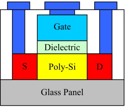
Fig. 1-1. The cross-section view of polycrystalline-silicon thin-film
transistor.
Chapter 2
Investigation of HfO
2/Poly-Si Interfacial Layer on CMOS
Low-Temperature Polycrystalline-Silicon Thin-Film
Transistor, Including O
2, N
2, NH
3Plasma Surface Treatment
2.1 Impacts of HfO2/Poly-Si Interfacial Layer on CMOS
Low-Temperature Polycrystalline-Silicon Thin-Film Transistor
with HfO2 Gate Dielectric
2.1.1 Introduction
As mentioned in Chapter 1.1, low-temperature polycrystalline silicon thin-film transistors (LTPS-TFTs) have been used for active-matrix liquid crystal displays (AMLCDs) and system-on-panel (SOP) on glass substrate as pixel switch devices and driving integrated circuits instead of amorphous silicon [2.1]-[2.6] due to that the field effect mobility μEF in polycrystalline silicon is significantly higher (by two orders of magnitude) than that in amorphous silicon [2.6]. So that complementary metal-oxide-semiconductor (CMOS) devices with reasonably high drive currents can be achieved in polycrystalline silicon. However, the highest temperature of TFTs manufacture process for the application of SOP is limited to the melting point of glass substrate. Consequently, it is difficult to develop high-performance LTPS-TFTs with low threshold voltage VTH, low subthreshold swing S.S. and high driving current IDsat to drive the liquid crystal of large area panel. Therefore, high-performance TFTs with high driving current IDsat, low gate leakage current IG, low threshold voltage VTH and subthreshold swing S.S. are required urgently. In order to enhance the driving current
of TFTs and break through this challenge, a thin gate oxide must be used to increase the gate capacitance density. However, a higher gate leakage current would be introduced when the thickness of gate oxide becomes thinner. In addition, low quality deposited low-temperature SiO2 (like plasma enhanced chemical vapor deposition or PECVD-SiO2) is generally employed as the gate dielectric of the conventional LTPS-TFT. Comparing with low quality deposited low-temperature SiO2, low temperature deposited high-κ gate dielectric could have better quality and be more suitable for the replacement of the conventional low temperature SiO2. Many high-κ dielectrics have been used to reduce gate leakage current and to increase transconductance Gm [2.7]-[2.14]. Among these dielectric materials, HfO2 is the most promising candidate of future high-κ gate dielectric material due to its high permittivity (~ 25) and thermal stability with poly-Si [2.11]-[2.14]. In this Chapter, a high performance LTPS-TFT with HfO2 gate dielectric is demonstrated.
For the application of system-on-panel (SOP) and three-dimension circuit integration, complementary metal-oxide-semiconductor (CMOS) LTPS-TFTs should be studied simultaneously. In this Chapter, the CMOS LTPS-TFTs with HfO2 gate dielectric are demonstrated. In addition, the growth of a SiO2-like interfacial layer (IL) at high-κ/poly-Si interface is observed while the high-κ materials are deposited on the poly-Si surface [2.8]-[2.12]. In this Chapter, the impacts of the IL on the electrical characteristics of LTPS-TFT are specified and compared with conventional CMOS LTPS-TFTs.
In addition to the employment of HfO2 gate dielectric, the oxygen plasma treatment has been proposed to improve the electrical characteristics of TFTs [2.15][2.16]. The improvements of TFTs are due to the defects passivation of grain boundaries and good quality of the oxide grown by oxidizing the poly-Si surface by oxygen plasma [2.15][2.16]. In this Chapter, the oxygen plasma is also used to study
the impact of IL on CMOS LTPS-TFTs.
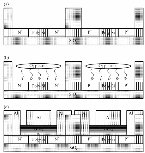
2.1.2 Fabrication Process
The fabrication of devices started by depositing a 50-nm undoped amorphous Si (α-Si) layer at 550°C in a low-pressure chemical vapor deposition system on Si wafers capped with a 500-nm thermal oxide layer. Then the 50-nm α-Si layer was recrystallized by solid-phase crystallization process at 600°C for 24-h in a N2 ambient. Then a 500-nm plasma-enhanced chemical vapor deposition oxide (PECVD-SiO2) was deposited at 300°C for device isolation. The device active region was formed by patterning and etching the isolation oxide. As shown in Fig. 2-1(a), the source and drain regions (S/D) in the active device region was implanted with phosphorus (15 keV at 5 x 1015 cm-2) and boron (10 keV at 5 x 1015 cm-2) for N- and P-channel LTPS-TFT, respectively. The S/D was activated at 600°C for 24-h annealing in a N2 ambient. Then oxygen plasma surface treatment was performed for 0, 5, and 15 min at 300°C with a power density of 1.6-mW/cm2 in O2, NH2 and NH3 gas as shown in Fig. 2-1(b). The flow-rate was 100-sccm at pressure of 67 Pa. A 50-nm HfO2 with effective oxide thickness EOT ~ 10.8-nm was deposited by electron-beam evaporation system at room temperature. In addition, a 49.3-nm PECVD-SiO2 was deposited at 300°C as the gate dielectric of conventional CMOS LTPS-TFTs, which are used to compare with CMOS LTPS-TFTs with HfO2 gate dielectric. After the patterning of S/D contact holes, aluminum was deposited by thermal evaporation system as the gate electrode and S/D contact pad. Finally, the TFT devices were completed by the contact pad definition as shown in Fig. 2-1(c). Devices with gate length (L) and width (W) of 10 and 100 μm are measured. The threshold voltage VTH is defined as the
field effect mobility μFE is extracted from the maximum transconductance (Gm).
2.1.3 Discussion of Impacts of Interfacial Layer on LTPS-TFT with
HfO2 Gate Dielectric, Including O2 Plasma Surface Treatment
Figure 2-2 shows the transfer characteristics (ID-VG and field effect mobility μFE) of CMOS HfO2 LTPS-TFTs without oxygen plasma surface treatment. Some important parameters of CMOS HfO2 LTPS-TFTs without oxygen plasma surface treatment and conventional CMOS LTPS-TFTs with SiO2 gate dielectric are all listed in Table 2-I. The threshold voltage VTH and subthreshold swing S.S. are reduced significantly while the SiO2 gate dielectric is replaced by HfO2. Larger gate capacitance density, which is achieved by replacing SiO2 gate dielectric by HfO2 due to higher relative dielectric constant of HfO2, can attract more carriers with a smaller gate voltage to turn on the LTPS-TFTs. In addition, CMOS LTPS-TFTs with HfO2 gate dielectric have higher electron and hole field effect mobility μFE than CMOS LTPS-TFTs with SiO2 gate dielectric. It indicates that the native growth of a SiO2-like IL between the HfO2 and poly-Si has better interface quality than deposited-SiO2/poly-Si interface [2.9]-[2.12]. Because the poly-Si channel film has a rough Si surface and lots of dangling bonds and strain bonds in the surface of poly-Si channel film, the native growth SiO2-like IL of HfO2 LTPS-TFT can terminate these defects and lead to better performance of LTPS-TFT.
For the characteristics of CMOS LTPS-TFTs with HfO2 gate dielectric as shown in Table 2-I and Fig. 2-2, the hole field effect mobility μFE is higher about 130.4 % than electron field effect mobility μFE, which is different from the conventional CMOS LTPS-TFTs with SiO2 gate dielectric that the hole field effect mobility μFE is lower about 24.1 % than electron field effect mobility μFE. It means that the IL of
HfO2/IL/poly-Si has different characteristics from deposited-SiO2/poly-Si. It is well known that the field effect carrier mobility μFE is dominated by the trap states near band tail region [2.17]. Higher hole field effect mobility μFE than electron field effect mobility μFE for HfO2 LTPS-TFTs indicates that there are less tail trap states near the valence band than tail trap states near conduction band. It implies that the native growth SiO2-like IL of HfO2/poly-Si interface can terminate both tail state traps density near conduction band and valence band, and more traps density near valence band are terminated than traps density near conduction band. Figure 2-3 shows the output characteristics (the ID-VD curve) of CMOS LTPS-TFTs with HfO2 gate dielectric. Significant higher driving current of P-channel HfO2 LTPS-TFT than N-channel HfO2 LTPS-TFT is obtained, which consists with the behavior of field effect mobility μFE of HfO2 LTPS-TFTs. It indicates that P-channel LTPS-TFT is more suitable for the driving device of display pixel than N-channel LTPS-TFT if HfO2 material is used as the gate dielectric of LTPS-TFT.
In addition to the intrinsic characteristics of LTPS-TFTs with HfO2 gate dielectric, oxygen plasma surface treatment is employed to study the impacts of growth-SiO2 by oxygen plasma on the CMOS LTPS-TFT with HfO2 gate dielectric. Figures 2-4 and 2-5 show the transfer characteristics (ID-VG and field effect mobility μFE) of N-channel and P-channel HfO2 LTPS-TFTs, respectively, with and without oxygen plasma surface treatment. Some important parameters of CMOS HfO2 LTPS-TFTs with and without oxygen plasma surface treatment are also listed in Table 2-II. The electron field effect mobility μFE is enhanced with the increase of oxygen plasma time, which indicates the tail trap states near conduction band of HfO2/poly-Si interface are passivated to enhance the electron field effect mobility μFE about 46.0 % and 92.4 % for 5-min and 15-min oxygen plasma time, respectively. However, the hole field effect mobility μFE is reduced while the oxygen plasma is performed for 5
min, which indicates the tail trap states near valence band of HfO2/poly-Si interface are generated after oxygen plasma surface treatment. When the oxygen plasma is performed for 15-min, the hole field effect mobility μFE is higher than the hole field effect mobility μFE of 5-min oxygen plasma treatment. It indicates different effects of oxygen plasma surface treatment. While the oxygen plasma surface treatment is initially performed for a short time, the oxygen diffused slowly and reacted with poly-Si to form a Si-O rich interfacial layer of HfO2/SiO2/poly-Si [2.16][2.18][2.19]. While the oxygen plasma treatment is performed for a long time, the oxygen atom can diffuse into the poly-Si channel to passivate the defects of grain boundaries [2.15][2.16]. Therefore, the impact of oxygen plasma surface treatment could be deduced that the effect of interfacial layer growth is dominant for the first 5-min oxygen plasma step. It results in the elimination of tail trap states of HfO2/poly-Si interface near the conduction band and the generation of tail trap states of HfO2/poly-Si interface near the valence band to enhance the electron field effect mobility μFE and reduce the hole field effect mobility μFE. After a long time of oxygen plasma treatment, the defects passivation of poly-Si channel is dominant, resulting in both electron and hole field effect mobility μFE are enhanced simultaneously.
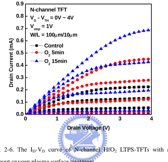
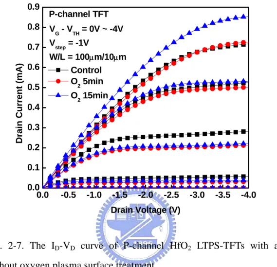
Figures 2-6 and 2-7 show the ID-VD curve of N-channel and P-channel HfO2 LTPS-TFTs with and without oxygen plasma surface treatment. From Fig. 2-7, the drain current at VD =4V of P-channel HfO2 LTPS-TFT with 5-min oxygen plasma
surface treatment is lower than the HfO2 LTPS-TFT without oxygen plasma surface treatment at VG−VTH ≤3V . However, the drain current at VD =4V of P-channel HfO2 LTPS-TFT with 5-min oxygen plasma surface treatment is higher than the HfO2 LTPS-TFT without oxygen plasma surface treatment at VG−VTH ≥4V even the
plasma surface treatment is lower than HfO2 LTPS-TFT without oxygen plasma surface treatment. The same trend could be observed for P-channel HfO2 LTPS-TFT with 15-min oxygen plasma surface treatment that the drain current at VD =4V of P-channel HfO2 LTPS-TFT with 15-min oxygen plasma surface treatment is lower than HfO2 LTPS-TFT without oxygen plasma surface treatment at VG −VTH ≤2V
and higher at VG−VTH ≥3V . We define the saturation current ID(sat) as the drain
current at VG −VTH =VD =4V as shown in Table 2-II. The P-channel LTPS-TFT
with oxygen plasma treatment shows a lower drain current at small VG and a higher
drain current at large VG as shown in Fig. 2-7. Figures 2-8 and 2-9 show the
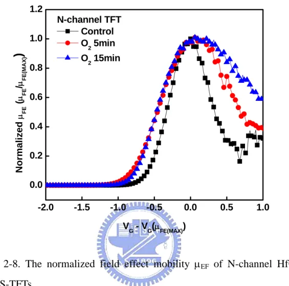
normalized field effect mobility μEF of N-channel and P-channel HfO2 LTPS-TFTs, respectively. It is noted that the field effect mobility μEF reduction is improved after the oxygen plasma treatment at highVG . As described above, the oxygen plasma can
passivate the defect trap states of poly-Si channel film and improve the interface quality of HfO2/poly-Si interface, resulting in the reduction of phonon scattering. Therefore, the drain current of P-channel LTPS-TFT with oxygen plasma treatment is lower at small VG due to lower μEF and higher at large VG due to the
improvement of phonon scattering.
2.1.4 Summary
CMOS LTPS-TFTs with HfO2 gate dielectric are demonstrated in this Chapter. The effects of HfO2/poly-Si interfacial layer on the electrical characteristics of CMOS LTPS-TFTs are also specified. In addition, the impacts of oxygen plasma surface treatment on CMOS LTPS-TFTs with HfO2 gate dielectric are investigated. Not only
the change of interfacial layer characteristics, but also the defects passivation of poly-Si channel film is observed. In conclusion, oxygen plasma surface treatment can improve the driving current of CMOS LTPS-TFTs with HfO2 gate dielectric due to the passivation of interface trap states and grain boundaries of poly-Si channel film. The combination of HfO2 gate dielectric and oxygen plasma surface treatment would be very suitable for the application of three-dimension circuit integration and SOP.
2.2 Characteristics of HfO2/Poly-Si Interfacial Layer with N2 and
NH3 Plasma Surface Treatment on Low-Temperature
Polycrystalline-Silicon Thin-Film Transistor with HfO2 Gate
Dielectric
2.2.1 Introduction
After the discussion of Chapter 2.1, characteristics of the native-growth HfO2/poly-Si interfacial layer of HfO2 LTPS-TFT have been studied comprehensively. However, the trap states still exist among the polycrystalline-silicon in spite of the employment of high-κ gate dielectrics without any defects passivation methods. The NH3 plasma post-treatment is the most general method to passivate the trap states of the polycrystalline-silicon channel film for conventional TFTs [2.20][2.21]. Hence, the impacts of NH3 plasma treatment on LTPS-TFT with high-κ gate dielectric would be worth to study. In order to distinguish the passivation effects of hydrogen H and nitrogen N, N2 plasma surface treatment would also be done to compare with NH3 plasma surface treatment. In this Chapter the HfO2 gate dielectric LTPS-TFT with N2 and NH3 surface plasma treatment is demonstrated.
2.2.2 Discussion of Impacts of N2 and NH3 Plasma Surface
Treatment on Low-Temperature Polycrystalline-Silicon
Thin-Film Transistor with HfO2 Gate Dielectric
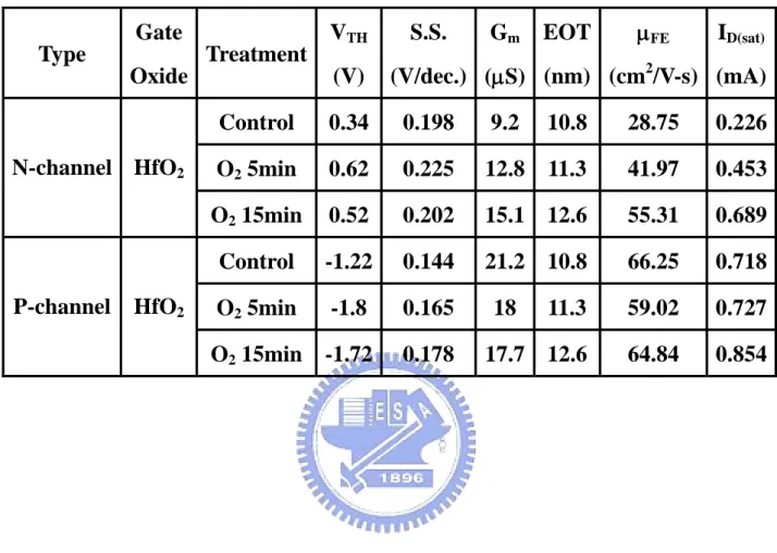
The device fabrication process with N2 and NH3 plasma surface treatment has described in section 2.1.2. Figures 2-10 and 2-11 show the transfer characteristics (ID-VG and transconductance Gm) of LTPS-TFT with HfO2 gate dielectric after N2 and NH3 plasma surface treatment for 5-min and 15-min, respectively. The important device parameters of LTPS-TFTs are listed in the Table 2-III. The subthreshold swing S.S. of device shows an improvement of 8.6 % and 9.6 % with N2 plasma surface treatment for 5-min and 15-min, respectively. Moreover, field effect mobility μFE of device also show an increase of 36.1 % and 74.4 % with N2 plasma surface treatment for 5-min and 15-min, respectively. It is known that subthreshold swing S.S. and field effect mobility μFE are related to the dangling-bond deep trap states and the strain-bond tail trap states of the polycrystalline-silicon channel [2.17], respectively. The significant increase on field effect mobility μFE indicates that nitrogen has better passivation effect on strain-bond tail trap states than on dangling-bond deep trap states. On the other hand, devices show 9.1 % and 21.2 % subthreshold swing S.S. improvement with NH3 plasma surface treatment for 5-min and 15-min, respectively. In addition, 5-min and 15-min NH3 plasma surface treatment show 50.0 % and 108.5 % field effect mobility μFE improvement, respectively. It is found that the improvement of subthreshold swing S.S. is on the same level by either 5-min N2 or NH3 plasma treatment. This implies hydrogen from NH3 has no significant contribution to the improvement of subthreshold swing S.S. for such a short 5-min. On the contrary, devices with a longer 15-min NH3 plasma exhibit more subthreshold swing S.S. improvement, indicating that more passivation effect on the dangling-bond deep trap states due to the contribution of hydrogen. Devices with either 15-min N2 or
NH3 plasma show significant field effect mobility μFE improvement, indicating good passivation on strain-bond tail states can be achieved by both plasma treatments. Figures 2-12 and 2-13 show the output characteristics (ID-VD) of LTPS-TFT with HfO2 gate dielectrics after N2 and NH3 plasma surface treatment for 5-min and 15-min, respectively. For 5-min, N2 plasma and NH3 plasma show 165.0 % and 91.3 % driving saturation current ID_sat enhancement at VG – VTH = 4V and VD = 5V as shown in Table 2-III and Fig. 2-12. The 5-min N2 plasma surface treatment shows a smaller field effect mobility μFE improvement and higher ID_sat enhancement than 5-min NH3 plasma surface treatment.
Figures 2-14 and 2-15 show the normalized μEF of HfO2 LTPS-TFTs with N2 and NH3 plasma surface treatment. It is noted that the μEF reduction rate after the peak is improved using surface plasma treatment at high VG. This improvement is due to the reduced surface roughness scattering [2.22]. N2 plasma surface treatment has more improvement on surface roughness scattering than NH3 plasma, resulting in a higher driving saturation current ID_sat for 5-min. The surface roughness scattering are improved further, leading to 217.0 % and 219.6 % improvement in driving saturation current for 15-min N2 and NH3 plasma surface treatment, respectively.
High performance LTPS-TFT with low threshold voltage VTH ~ 0.45 V, excellent subthreshold swing S.S. ~ 0.179 V/decade and high field effect mobility μFE ~ 51.25 cm2/V-s is obtained by using HfO2 gate dielectric and 15-min N2 plasma surface treatment. In addition, high performance LTPS-TFT with low threshold voltage VTH ~ 0.33 V, excellent subthreshold swing S.S. ~ 0.156 V/decade and high field effect mobility μFE ~ 61.25 cm2/V-s is also obtained by using HfO2 gate dielectric and 15-min NH3 plasma surface treatment.
2.2.3 Summary
In this Chapter, high performance LTPS-TFT with HfO2 gate dielectric has been fabricated. In order to enhance the performance of LTPS with high-κ gate dielectric, two kinds of plasma, N2 and NH3, are employed. Subthreshold swing S.S., field effect mobility μFE and driving saturation current are all significantly improved after N2 and NH3 plasma surface treatment.