國
國
國
國 立
立
立
立 交
交
交
交 通
通
通
通 大
大
大
大 學
學
學
學
工學院影像顯示科技產業研發碩士班
碩士論文
碩士論文
碩士論文
碩士論文
非晶矽薄膜電晶體在汲極
非晶矽薄膜電晶體在汲極
非晶矽薄膜電晶體在汲極
非晶矽薄膜電晶體在汲極直
直
直
直流或
流或
流或
流或交
交
交
交流
流
流
流
操作
操作
操作
操作下的
下的
下的
下的劣化行為
劣化行為
劣化行為
劣化行為研究
研究
研究
研究
Degradation Behavior of Hydrogenated
Amorphous Silicon TFTs under Drain
DC/AC Operation
研
研
研
研 究
究
究
究 生
生
生
生 : 蔡明憲
蔡明憲
蔡明憲 Ming-Hsien Tsai
蔡明憲
指導教授
指導教授
指導教授
指導教授 : 戴亞翔
戴亞翔
戴亞翔 博士
戴亞翔
博士
博士 Dr. Ya-Hsiang Tai
博士
中華民國 九十六 年 十二 月
II
非晶矽薄膜電晶體在汲極
非晶矽薄膜電晶體在汲極
非晶矽薄膜電晶體在汲極
非晶矽薄膜電晶體在汲極直流或交流操作下的
直流或交流操作下的
直流或交流操作下的
直流或交流操作下的
劣化行為研究
劣化行為研究
劣化行為研究
劣化行為研究
Degradation Behavior of Hydrogenated Amorphous
Silicon TFTs under Drain DC/AC Operation
研 究 生 : 蔡明憲 Student : Ming-Hsien Tsai
指導教授 : 戴亞翔
博士 Advisor : Dr. Ya-Hsiang Tai
國
國
國
國
立
立
立
立
交
交
交
交
通
通
通
通
大
大
大
大
學
學
學
學
工學院影像顯示科技產業研發碩士班
工學院影像顯示科技產業研發碩士班
工學院影像顯示科技產業研發碩士班
工學院影像顯示科技產業研發碩士班
碩
碩
碩
碩
士
士
士
士
論
論
論
論
文
文
文
文
A Thesis
Submitted to College of Engineering
National Chiao Tung University
in Partial Fulfillment of the Requirements
for the Degree of
Master
in
Industrial Technology R & D Master Program of
Image Display Technologies
December 2007
Hsinchu, Taiwan, Republic of China
III
非晶矽薄膜電晶體在汲極直流或交流操作下的
非晶矽薄膜電晶體在汲極直流或交流操作下的
非晶矽薄膜電晶體在汲極直流或交流操作下的
非晶矽薄膜電晶體在汲極直流或交流操作下的
劣化行為研究
劣化行為研究
劣化行為研究
劣化行為研究
研究生: 蔡明憲 指導教授: 戴亞翔 博士
國立交通大學
國立交通大學
國立交通大學
國立交通大學
工學院影像顯示科技產業研發碩士班
工學院影像顯示科技產業研發碩士班
工學院影像顯示科技產業研發碩士班
工學院影像顯示科技產業研發碩士班
摘要
摘要
摘要
摘要
非晶矽薄膜電晶體(a-Si:H TFTs)在閘極直流或交流電壓操作下的劣化機制 已被廣泛的討論;然而在更先進的應用中,非晶矽薄膜電晶體不再只是扮演畫素 開關的角色,而是逐漸朝向驅動元件的方向發展,和傳統應用不同的地方在於非 晶矽薄膜電晶體在驅動電路中會同時受到閘極和汲極信號的作用;因此,其在閘 極和汲極信號下的劣化行為值得被深入研究。 在本論文中,非晶矽薄膜電晶體在閘極偏壓(On region)的汲極直流操作以及 在閘極接地(Off region)的汲極直流操作下的劣化行為被提出來探討;另外,將 汲極直流信號改為具有不同峰值電壓、頻率、開啟比率的交流信號操作下的劣化 行為亦同時被提出來做深入的研究。 關於直流操作實驗的結果顯示:在閘極偏壓的汲極直流操作下,劣化會隨著 汲極電壓的增加而減輕;這是肇因於當汲極電壓增加時電晶體通道內的載子會因 閘極和汲極間相對電壓的降低而隨之減少,因而造成劣化的減輕;然而當閘極接 地的汲極直流操作下,趨勢卻是相反;在此操作情形下隨著汲極電壓的增加,劣 化會顯得更為嚴重;同時發現在閘極接地的汲極直流操作下,電晶體內的劣化位
IV 置將呈現不對稱分布,此現象可透過正向和反向汲極電流的測量而觀察到。 汲極交流信號操作的實驗結果顯示:劣化的情形類似於汲極直流的操作,而 在頻率相關的實驗結果中,在閘極偏壓的汲極交流操作下,電晶體劣化和交流信 號的頻率無明顯相關,主要是因為通道內的載子為具有快速累積能力的電子;相 對於此,在閘極接地的汲極交流操作下,劣化則和頻率有明顯的相關;除了交流 頻率的實驗,在汲極交流信號開啟比率的實驗結果中,發現在特定頻率下無論閘 極偏壓的施加與否,汲極交流信號的有效操作時間將會影響整個劣化的行為。 在完成所有實驗後,根據實驗結果,我們在論文中提出了一個具有線性組合 的劣化模型;藉由此模型的運用,我們可以預估施加不同電壓準位、不同頻率, 不同開啟比率的汲極交流信號,經過任何操作時間後的臨界電壓變化;而量測的 結果顯示此模型具有相當高的可靠性,可用以預測非晶矽薄膜電晶體電路在同時 受到閘極和汲極信號操作下的可靠度以及電路的壽命。
V
Degradation Behavior of Hydrogenated Amorphous
Silicon TFTs under Drain DC/AC Operation
Student : Ming-Hsien Tsai Advisor : Dr. Ya-Hsiang Tai
Industrial Technology R & D Master Program of
Image Display Technologies
National Chiao Tung University
Abstract
The degradation mechanisms of a-Si:H TFTs under gate DC (direct current) and
AC (alternating current) stress had been widely discussed. However, with the
extending of advanced applications, a-Si:H TFTs no longer play the roles as switch
elements but driving devices. Unlike traditional application, TFTs in driving circuits
are subjected to signals in both gate and drain terminals. Therefore, the degradation
behavior under both drain and gate stress should be understood in detail.
In this thesis, the degradation of a-Si:H TFTs under drain DC stress in both on
(with gate voltage bias) and off (with gate grounded) regions has been investigated. In
addition, the degradation under on and off region drain AC stress with different peak
levels, frequencies and duty ratios is also studied. It is found that the degradation
decreases as drain voltage level increases for on region drain DC stress. The carriers
induced in the channel are reduced with increasing drain bias, which result in the
decreasing of degradation. But for off region drain DC stress, we have observed the
contrary results. The degradation behavior is similar to negative gate DC stress and
VI
degradation in TFTs under off region drain stress is not symmetric. Different
degradation amplitude between forward measurement and reverse measurement is
observed.
For drain AC stress, the degradation shows similar behavior as drain DC stress.
It is found that the degradation has no obvious frequency dependence in on region
drain AC stress because of the carriers are electrons which have fast accumulation
ability. But it shows apparent frequency dependence when performing off region
drain AC stress. For the duty ratio experiment under low frequency, it is found that
the effective stress time will dominate in both on and off region drain AC stress.
Furthermore, base on the experiment result, a linear combination model has
been contributed in this thesis. By using this model, we can estimate the threshold
voltage shift under drain AC stress of different voltage levels, frequencies and duty
ratios after any stress time. With satisfied agreement of our real measured data, this
model has been proved to be very useful for the design of advanced a-Si:H circuits
VII
Acknowledgements
首先要感謝的是我的指導教授 戴亞翔博士;老師對學生無私的奉獻,無論 在生活上或學業上,時刻為學生著想;而在業界的工作經驗,前瞻的研究方向, 以及周全準確的判斷,總是能適時對學生的研究,形成很大的助力;對論文內容 的嚴謹要求,及費心修訂的苦心,更是令人感激;也因為老師的體諒,使我在學 業和家庭之間都能兼顧;在此,對老師致上最深的敬意。 接著要感謝學長姐們:士哲、彥甫,感謝你們的啟蒙指導,使我對研究方向 有了初步的了解;感謝浩麟、國烽、鈺函、可青、建焜、婉萍、俊文、娟姐,你 們親切的態度,讓我對實驗室逐漸感到熟悉;感謝晉煒、育德、偉倫、振業,跟 你們在一起,有歡笑有陽光,有你們的日子,總是特別溫暖。 感謝實驗室的同學及學弟妹們:長龍、曉嫻,兩年的相互扶持,沒有彼此, 總是能無私地分享研究生活的點滴經驗;小黑、首席、翔帥,在需要時總能不吝 伸出援手,積極的研究態度,也漸漸使實驗室的研究風氣,獲得顯著的向上提升; Leopard、騰瑞、紹文、國珮、耿維、思豪,你們為實驗室注入了一股活水,更 加速了整體論文研讀的速度,展望未來,DADS 將因你們的加入而發熱發光。 最要感謝的是我最親愛的家人們:我最愛的老婆琦樺,在交大的這段日子, 遙遠的距離,也因為妳的支持和體諒,讓我能無後顧之憂的完成這段學業,更感 謝你對兒子的照顧,老婆辛苦了!也感謝兒子承憑,因為你的來臨,把拔能堅定 信念完成論文,希望的是能給你一個很好的未來;也感謝母親和大哥、大嫂,你 們的關心,伴隨著我成長。 最後再感謝我的口試委員:劉柏村教授、簡昭欣教授和劉漢文教授,感謝你 們的建議和指導;也感謝交大和奇美電子,讓我有機會在如此優良的環境中,順 利完成論文並取得碩士學位。感恩
明憲 2007.12.25VIII
Contents
Chinese Abstract
……….……… IIIEnglish Abstract
………..…………..………. VAcknowledgement
……..………...………...…. VIIContents
...………... VIIITable Captions
……….... XFigure Captions
……….... XIChapter 1
Introduction
1.1 Overview of Hydrogenated Amorphous Silicon Thin Film Transistors
(A-Si :H TFTs) ………....……….. 1
1.2 Review of Studies on a-Si:H TFTs under DC and AC Stress .…………. 3
1.2.1 DC Stress ………....……….. 3 1.2.2 AC Stress ………....……….. 5 1.2.2.1 Pulse-Width Dependence ………...……….……….. 6 1.2.2.2 Duty-Cycle Dependence ………...……….…….….. 7 1.3 Motivation ………...……….…...…….. 8 1.4 Thesis Organization ………...…...……….……….. 10
Chapter 2 Experiments
2.1 Procedures of Fabricating A-Si :H TFTs ………...……….………... 132.2 Extraction of Device Electrical Parameters ………...………….………... 14
2.2.1 Determination of the Threshold Voltage (VTH) ………...….……... 14
2.2.2 Determination of the Sub-threshold Swing (SS.) ………....……... 14
2.3 Stress Conditions ………...…...……... 15
IX
2.3.2 Drain AC Stress ………...….…...…... 17
2.3.2.1 Peak Level Dependence ………...….……... 18
2.3.2.2 Frequency Dependence ………....….……... 19
2.3.2.3 Duty Ratio Dependence ………...….……... 20
Chapter 3 Degradation under Drain DC Stress
3.1 Degradation under Drain DC Stress in ON Region ………... 213.1.1 Voltage Level Dependence ………...….……... 21
3.1.2 Damage Region confirmation ………...….……... 26
3.2 Degradation under Drain DC Stress in OFF Region ………...….…….... 30
3.2.1 Voltage Level Dependence ………...….……... 30
3.2.2 Damage Region confirmation ………...….……... 33
Chapter 4
Degradation under Drain AC Stress
4.1 Degradation under Drain AC Stress in ON Region ………...…... 384.1.1 Peak Level Dependence ………...….……... 38
4.1.2 Frequency Dependence ………...….….…... 48
4.1.3 Duty Ratio Dependence ………...….……... 53
4.2 Degradation under Drain AC Stress in OFF Region ………...….…... 59
4.2.1 Peak Level Dependence ………...….……... 59
4.2.2 Frequency Dependence ………...….……... 65
4.2.3 Duty Ratio Dependence ………...….……... 68
Chapter 5
Conclusions
………...…...……... 71X
Table Captions
Chapter 2
Table 2-1. Experiment conditions of drain DC stress. ... 15
Table 2-2. Experiment conditions of drain AC stress - Peak Level Dependence. ... 18
Table 2-3. Experiment conditions of drain AC stress - Frequency Dependence. ... 19
XI
Figure Captions
Chapter 1
Fig.1-1. Evolution of Id-Vg characteristics with various bias stress times.
[Jpn. J. Appl. Phys. Vol. 37, pp.4706, 1998.] ... 4
Fig.1-2. Evolution of Id-Vg characteristics induced by pulsed positive and negative gate bias stress. [Jpn. J. Appl. Phys. Vol. 37, pp.4707, 1998.] ... 5
Fig.1-3. Threshold voltage shift (∆VT) versus effective stress time induced by positive and negative gate-bias stress with different gate pulse-width. [Jpn. J. Appl. Phys. Vol. 37, pp.4707, 1998.] ... 6
Fig.1-4. Threshold voltage shift (∆VT) versus stress time for positive and negative gate-bias stress with different duty-cycles. [Jpn. J. Appl. Phys. Vol. 37, pp.4710, 1998.] ... 8
Fig. 1-5. The block diagram of an active matrix display. ... 9
Fig. 1-6. The integration of peripheral circuits in a display achieved by a-Si:H TFTs. ... 10
Chapter 2
Fig. 2-1. The cross-section views of a-Si:H TFTs. ... 13Fig. 2-2. TFT under drain DC stress with gate bias and source grounded. ... 16
Fig. 2-3. Waveform and definition of the AC signal. ... 17
Fig. 2-4. TFT under drain AC stress with gate DC bias and source grounded. ... 18
Chapter 3
Fig. 3-1(a). ON region VDS dependence of ID-VG degradation. ... 22Fig. 3-1(b). ON region VDS dependence of VTH Shift. ... 22
XII
Fig. 3-2. VTH shift versus stress time for ON region drain DC stress. ... 24
Fig. 3-3. ON region drain DC stress. (As the drain bias increases, the relative VGD is decreased while VGS remains unchanged.) ... 25
Fig. 3-4. Dependence of ∆VT on VGS and VGD from the report of Karim et al. [IEEE ELECTRON DEVICE LETTERS, Vol. 25, No. 4, April 2004.] ... 25
Fig. 3-5(a). I-V curve of ON region 5V drain DC stress with forward and reverse measurement under VDS=10V. ... 26
Fig. 3-5(b). VTH shift versus stress time of ON region 5V drain DC stress with forward and reverse measurement under VDS=10V. ... 27
Fig. 3-6(a). I-V curve of ON region 30V drain DC stress with forward and reverse measurement under VDS=10V. ... 27
Fig. 3-6(b). VTH shift versus stress time of ON region 30V drain DC stress with forward and reverse measurement under VDS=10V. ... 28
Fig. 3-7(a). Forward saturation current of ON region drain DC stress. (Measured @ VDS=10V) ... 29
Fig. 3-7(b). Reverse saturation current of ON region drain DC stress. (Measured @ VDS=10V) ... 29
Fig. 3-8(a). OFF region VDS dependence of ID-VG degradation. ... 30
Fig. 3-8(b). OFF region VDS dependence of VTH Shift. ... 31
Fig. 3-8(c). OFF region VDS dependence of SS. Change. ... 31
Fig. 3-9. Absolute value of VTH shift versus stress time for OFF region drain DC stress. ... 32
Fig. 3-10. OFF region drain DC stress. (With no bulk voltages taking into consideration, the OFF region drain DC stress is like negative gate DC stress on single side of the TFT.) ... 33
Fig.3-11(a). I-V curve of OFF region drain DC stress with forward and reverse measurement under VDS=10V. ... 34
XIII
Fig.3-11(b). VTH shift versus stress time of OFF region drain DC stress with
forward and reverse measurement under VDS=10V. ... 34
Fig.3-12(a). Forward saturation current of OFF region drain DC stress. (Measured @ VDS=10V) ... 35
Fig.3-12(b). Reverse saturation current of OFF region drain DC stress. (Measured @ VDS=10V) ... 35
Fig.3-13(a). I-V curve of OFF region drain DC stress with linear mode (VDS=1V) and saturation (VDS=10V) mode measurement. ... 37
Fig.3-13(b). VTH shift versus stress time of OFF region drain DC stress with linear mode (VDS=1V) and saturation mode (VDS=10V) measurement. ... 37
Chapter 4
Fig. 4-1(a). ON region drain AC stress peak level dependence of ID-VG degradation.39 Fig. 4-1(b). ON region drain AC stress peak level dependence of VTH Shift. ... 40Fig. 4-1(c). ON region drain AC stress peak level dependence of SS. Change. ... 40
Fig. 4-2. VTH shift versus stress time for ON region drain AC stress. ... 41
Fig. 4-3. ON region drain AC stress. ... 42
Fig. 4-4. Comparison for VTH Shift of ON region drain AC and DC stress versus VDS peak levels with fitted result. ... 43
Fig. 4-5. Comparison between fitted result and measured data of equation (4.8). .45 Fig. 4-6(a). I-V curves of ON region 0~5V drain AC stress with forward and reverse measurements under VDS=10V. ... 46
Fig. 4-6(b). VTH shift versus stress time of ON region 0~5V drain AC stress with forward and reverse measurements under VDS=10V. ... 46
Fig. 4-7(a). I-V curves of ON region 0~30V drain AC stress with forward and reverse measurements under VDS=10V. ... 47
Fig. 4-7(b). VTH shift versus stress time of ON region 0~5V drain AC stress with forward and reverse measurements under VDS=10V. ... 47
XIV
Fig. 4-8(a). ON region linear mode drain AC stress frequency dependence of ID-VG
degradation. ... 48
Fig. 4-8(b). ON region linear mode drain AC stress frequency dependence of VTH
shift. ... 49
Fig. 4-8(c). ON region linear mode drain AC stress frequency dependence of SS.
change. ... 49
Fig. 4-9(a). ON region saturation mode drain AC stress frequency dependence of
ID-VG degradation. ... 50
Fig. 4-9(b). ON region saturation mode drain AC stress frequency dependence of VTH
shift. ... 51
Fig. 4-9(c). ON region saturation mode drain AC stress frequency dependence of SS.
change. ... 51
Fig. 4-10. The equivalent circuit of a-Si:H TFT ON region drain AC stress. ... 52
Fig.4-11(a). ON region linear mode drain AC stress duty ratio dependence of ID-VG
degradation. ... 53
Fig.4-11(b). ON region linear mode drain AC stress duty ratio dependence of VTH
shift. ... 54
Fig.4-11(c). ON region linear mode drain AC stress duty ratio dependence of SS.
change. ... 54
Fig.4-12(a). ON region saturation mode drain AC stress duty ratio dependence of
ID-VG degradation. ... 55
Fig.4-12(b). ON region saturation mode drain AC stress duty ratio dependence of VTH
shift. ... 56
Fig.4-12(c). ON region saturation mode drain AC stress duty ratio dependence of SS.
change. ... 56
Fig.4-13(a). ON region linear and saturation mode drain AC stress VDS duty ratio
XV
Fig.4-13(b). Comparison between fitted result and measured data of equation (4.9)
for different duty ratios. ... 58
Fig.4-14(a). OFF region drain AC stress peak level dependence of ID-VG degradation. ... 60
Fig.4-14(b). OFF region drain AC stress peak level dependence of VTH Shift. ... 60
Fig.4-14(c). OFF region drain AC stress peak level dependence of SS. Change. ... 61
Fig. 4-15. Absolute value of VTH shift versus stress time for OFF region drain AC stress. ... 61
Fig. 4-16. OFF region drain AC stress. ... 62
Fig. 4-17. Comparison for VTH Shift of OFF region drain AC and DC stress versus VDS peak levels with fitted result. ... 63
Fig.4-18(a). I-V curve of OFF region drain AC stress with forward and reverse measurements under VDS=10V. ... 64
Fig.4-18(b). VTH shift versus stress time of OFF region drain AC stress with forward and reverse measurements under VDS=10V. ... 64
Fig.4-19(a). OFF region drain AC stress frequency dependence of ID-VG degradation. ... 65
Fig.4-19(b). OFF region drain AC stress frequency dependence of VTH shift. ... 66
Fig.4-19(c). OFF region drain AC stress frequency dependence of SS. change. ... 66
Fig. 4-20. The equivalent circuit of a-Si TFT OFF region drain AC stress. ... 67
Fig.4-21(a). OFF region drain AC stress duty ratio dependence of ID-VG degradation. ... 68
Fig.4-21(b). OFF region drain AC stress duty ratio dependence of VTH shift. ... 69
Fig.4-21(c). OFF region drain AC stress duty ratio dependence of SS. change. ... 69
Fig. 4-22. OFF region drain AC stress VDS duty ratio dependence of VTH shift measured and fitted result. ... 70
1
Chapter 1
Introduction
1.1
Overview of Hydrogenated Amorphous Silicon
Thin Film Transistors (A-Si:H TFTs)
As the popularization of flat-panel displays grows up, liquid-crystal displays (LCDs) have become the most common system in many commercial applications. Hydrogenated amorphous silicon (a-Si:H) thin-film transistors (TFTs) is one of the extremely important electronic devices because of their numerous applications in liquid-crystal displays (LCDs).
The fabrication technology of a-Si:H TFTs is well established for large area panel these days. The major advantages that make this technology been widely used are its good electronic properties such as high photoconductivity [1-3], and the ability to achieve low cost fabrication at low temperature. Good uniformity of electronic characteristics over large area especially achieves it suitable for manufacturing large size electronic devices. Except active matrix liquid-crystal displays (AMLCDs) [4], a-Si:H TFTs have many other applications like x-ray imaging arrays [5], digital scanners, digital cameras, solar cells [6] and even flexible displays [7]. In most of these applications, a-Si:H TFTs function like simple switch elements. High resolution, long lifetime, low power consumption, and acceptable performance are required. A-Si:H TFTs have great benefits in application of large area devices. However, they present several design challenges. First, the electron mobility in a-Si:H is between 0.1 and 1.0 cm2/V-Sec which is approximately 1000X smaller than in
2
single-crystal silicon. This results in a corresponding reduction in current driving ability and speed. Second, only NMOS devices can be readily fabricated in a-Si:H technology is another important issue. This disadvantage gives a-Si:H a limit of developing in conventional VLSI technique, which is used to building on well-known CMOS design technique. Even more serious is the electrical instability of a-Si:H TFTs. This phenomenon has been extensively investigated to evaluate the reliability of TFT products as well as to understand the physics of amorphous silicon.
The most important instability in a-Si:H TFTs is the shift of threshold voltage caused by a prolonged application of gate bias stress. This threshold voltage shift will limit the use of the devices in some demanding applications and has been reasonably heeded. Furthermore, the sub-threshold behavior should also be concerned. Many reports indicate that the instability sources degrading the transfer characteristics of a-Si:H TFTs are composed of charge trapping and defect state creation [8,9]. The charge trapping in the slow state, which is dominant at high electric fields and/or long stress time, relates to trap sites in the silicon nitride (SiNx) gate insulator. In contrast, the defect state creation in the fast state, which is dominant at lower electric fields, associates with the breaking of Si-Si weak bonds in the a-Si:H layer and at the a-Si:H/SiNx interface as well as increasing the density of defect states[10]. The charge trapping shows logarithmic time and weak temperature dependence while the state creation presents power-law time and thermally activated temperature dependence. The electron or hole trapping rigidly shift the threshold voltages of the a-Si:H TFTs in opposite direction with only a little degradation of sub-threshold behavior. The created defect states can positively shift the threshold voltage but only the states with energy position in the upper part of the energy gap can degrade the sub-threshold behaviors of n-channel a-Si:H TFTs [11-13].
3
large area electric devices for decades. With the extending of applications, the instability of a-Si:H TFTs becomes a key concern of these advanced designs and is worhty to be researched.
1.2 Review of Studies on a-Si:H TFTs under DC and
AC Stress
In order to make a-Si:H TFTs suitable for advanced circuits, besides the improvement of performance of a-Si:H TFTs, the improvement of reliability is also significant. Therefore, reliability testing and understanding of reliability mechanisms become more and more necessary.
1.2.1 DC stress
As mentioned in introduction, the creation of extra defect states in the band gap of a-Si:H and the charge trapping in the SiNx gate dielectric had been reported to be the two main mechanisms that can explain the electrical instabilities of a-Si:H TFTs. For transistors made with a siliconnitride gate insulator, the threshold voltage shift for low positive gate-bias is due to dangling-bond-state creation in the amorphous silicon layer. But in recent research, for low negative gate-bias, the threshold voltage shift is dominated by the bias-stress-induced removal of dangling-bond states. This is because the zero-bias Fermi energy position in nitride transistors are near the conduction band [14].
4
Fig.1-1. Evolution of Id-Vg characteristics with various bias stress times. [Jpn. J. Appl. Phys. Vol. 37, pp.4706, 1998.]
Fig.1-1. [15] shows the evolution of ID-VG characteristics for a regular a-Si:H TFTs under +20V and -20V steady-state gate-bias stress. As can be seen in this figure, an apparent right shift was obtained for the IV characteristics of +20V stress. From this report, Chiang et al. proposed the right shift was from the increase of the density of deep-gap states in a-Si:H, and also the charge trapping in the SiNx gate dielectric. The combination of these two mechanisms caused an additive effect in the shift of electron conduction characteristics [15].
For -20V stress, the IV characteristics show an obvious left shift with little distortion of sub-threshold behavior. This result corresponded to a decrease of deep-gap states in the a-Si:H. Similarly to the positive stress, charge trapping was also present and the left shift was a combination of these two mechanisms [15].
5
1.2.2 AC stress
In most applications, a-Si:H TFTs are operated under a pulsed gate-bias addressing. To understand the instability under AC bias stress is extremely important as well.
Fig.1-2. Evolution of Id-Vg characteristics induced by pulsed positive and negative gate bias stress. [Jpn. J. Appl. Phys. Vol. 37, pp.4707, 1998.]
Fig.1-2. [15] shows the evolution of ID-VG characteristics of a-Si:H TFTs during a positive and negative pulsed gate-bias stress with 50% duty-cycle and 10ms pulse-width at 70℃. Comparing with Fig. 1-1., it shows that, under positive gate-bias stress, pulsed and steady-state bias stress induced a similar evolution of IV characteristics. However, the left shift IV characteristics induced by negative pulsed gate-bias stress was apparently smaller than that induced by steady-state gate bias stress.
6
1.2.2.1 Pulse-Width Dependence
Fig.1-3. Threshold voltage shift (∆VT) versus effective stress time induced by positive and negative gate-bias stress with different gate pulse-width.
[Jpn. J. Appl. Phys. Vol. 37, pp.4707, 1998.]
Fig.1-3. [15] shows the threshold voltage shift (∆VT) versus effective stress time under both positive and negative bias-stress for different pulse conditions. The effective stress time was the accumulation time when the gate voltage was high. For positive pulsed gate-bias stress, ∆VT was slightly smaller than that for steady-state gate-bias stress and did not depend apparently on gate-bias pulse width. For negative pulsed gate-bias stress, ∆VT had strong pulse-width dependence- the wider the pulse width, the greater the magnitude of ∆VT.
From the same report [15], Chiang et al. proposed that, for positive pulsed gate-bias stress, during the OFF-cycle of the stress, some of the trapped charge and created states could be detrapped or relaxed. This could explain the smaller ∆VT of pulsed gate-bias stress than steady-state stress. Also, during the ON-cycle of positive
7
pulsed gate-bias stress, there would be a fast electron channel accumulation. Since the accumulation speed of electrons was much faster than the pulse-width, it would have very small pulse-width dependence. In contrast to positive pulsed gate-bias stress, the accumulated carriers of negative pulsed gate-bias stress were holes. The accumulation speed of holes was much slower than that of electrons and even slower than the stress pulse-width. With low concentration of carriers (holes) accumulation, there would not be a large degradation of IV characteristics. And this was the reason why ∆VT had strong pulse-width dependence when performing negative pulsed stress. Libsch et al. also proposed a RC time delay effect theory [16] to further explain this phenomenon.
1.2.2.2 Duty-Cycle Dependence
For duty-cycle dependence, Chiang et al. reported the following equations to describe the threshold voltage shift under pulsed gate-bias stress [15].
(1.1) (1.2 ) (1.3) Where VGH andVGL are the high and low gate-bias pulse-levels, respectively; VTi is the initial threshold voltage,
t
st is the stress time, A-, A+,α
-,α
+, β-, β+ and FPW are constants, and Dc is the duty cycle of the stressing voltage.They proposed that the total threshold voltage shift ∆VT±(
t
st) could be composed of threshold voltage shift induced by positive stress ∆VT﹢(t
st) and the threshold voltage shift induced by negative stress ∆VT﹣(t
st). The voltage shift of each pulsed gate-bias stress could be expressed as the effective steady-state stress duty with a8
fitting constant β except the frequency limit of negative pulsed gate-bias stress caused by the slow holes accumulation. Fig.1-4. shows a satisfactory fit between the calculated and experimental data.
Fig.1-4. Threshold voltage shift (∆VT) versus stress time for positive and negative gate-bias stress with different duty-cycles.
[Jpn. J. Appl. Phys. Vol. 37, pp.4710, 1998.]
1.3 Motivation
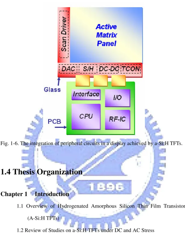
More recently, there has been significant progress in extending the applications of a-Si:H TFTs. For example, in order to reduce the number of interconnections to the display, it is desirable to integrate the row and column drivers in a-Si:H on the backplane as shown in Fig.1-5 and Fig.1-6. Row drivers can be designed with low duty cycle but column drivers cannot. Column drivers have much a higher duty cycle which accentuating the shift in threshold voltage with a further decrease in useful life time. Also, a-Si:H TFTs in the column driver act no longer switch TFTs but driver TFTs. Such application can require the device to withstand prolonged voltages at both the gate and drain terminals and as such, the instability becomes a key concern for
9 proper operation of the pixel circuit.
The instability mechanisms of a-Si:H TFTs under gate DC (direct current) bias stress and AC stress have been widely discussed. However, up to now, the instability of a-Si:H TFTs under drain stress has been paid much less attention. In this study, the degradation of n-channel a-Si:H TFTs under drain DC and AC stress with various voltage levels, signal frequencies, and duty-cycles was discussed to verify the degradation mechanism under drain stress.
10
Fig. 1-6. The integration of peripheral circuits in a display achieved by a-Si:H TFTs.
1.4 Thesis Organization
Chapter 1
Introduction
1.1 Overview of Hydrogenated Amorphous Silicon Thin Film Transistors (A-Si:H TFTs)
1.2 Review of Studies on a-Si:H TFTs under DC and AC Stress 1.2.1 DC Stress 1.2.2 AC Stress 1.2.2.1 Pulse-Width Dependence 1.2.2.2 Duty-Cycle Dependence 1.3 Motivation 1.4 Thesis Organization
11
Chapter 2 Experiments
2.1 Procedures of Fabricating A-Si :H TFTs 2.2 Extraction of Device Electrical Parameters
2.2.1 Determination of the Threshold Voltage (VTH)
2.2.2 Determination of the Sub-threshold Swing (SS.) 2.3 Stress Conditions
2.3.1 Drain DC Stress 2.3.2 Drain AC Stress
2.3.2.1 Peak Level Dependence 2.3.2.2 Frequency Dependence 2.3.2.3 Duty Ratio Dependence
Chapter 3 Degradation under Drain DC Stress
3.1 Degradation under Drain DC Stress in ON Region3.1.1 Voltage Level Dependence 3.1.2 Damage Region confirmation
3.2 Degradation under Drain DC Stress in OFF Region 3.2.1 Voltage Level Dependence
3.2.2 Damage Region confirmation
Chapter 4
Degradation under Drain AC Stress
4.1 Degradation under Drain AC Stress in ON Region 4.1.1 Peak Level Dependence4.1.2 Frequency Dependence 4.1.3 Duty Ratio Dependence
12 4.2.1 Peak Level Dependence 4.2.2 Frequency Dependence 4.2.3 Duty Ratio Dependence
Chapter 5
Conclusion
13
Chapter 2
Experiments
2.1 Procedures of Fabricating A-Si :H TFTs
The a-Si:H TFTs used in this thesis were the conventional bottom-gate inverted staggered structure and fabricated on the glass substrates. The cross-section views of a-Si:H TFTs are shown in Fig 2-1. After the deposition and patterning of gate metal on the glass substrates, three layers, i.e., silicon nitride (SiNx, 4000 Å), a-Si:H, and n+ a-Si:H films, were successively deposited in a plasma enhanced chemical vapor deposition (PECVD) system. After making the source/drain electrodes, the n+ a-Si:H region with length (L) of 5 µm and width (W) of 20 µm between the source/drain electrodes was etched off by a reactive ion etch. Then, a passivation layer was used to cap the channel region. All TFTs with the same dimension (W/L=20µm /5µm) will be used for instability testing in chapter 3 and chapter 4.
Fig. 2-1 The cross-section views of a-Si:H TFTs. Gate
SiNx (4000Å) a-Si:H
n+ a-Si:H
14
2.2 Extraction of Device Electrical Parameters
The methods of the typical electrical parameter extraction will be introduced in the following contents, including threshold voltage and sub-threshold swing.
2.2.1 Determination of the Threshold Voltage (V
TH)
The method to determine the threshold voltage in this thesis is the constant drain current method, which is adopted in most studies of a-Si:H TFTs. The threshold voltage is defined as the gate voltage which yields a normalized drain current (i.e. the threshold current). For the TFTs used in this thesis, the threshold current of 4 nA in linear region measurement (VDS=1V) and 40 nA in saturation region measurement (VDS=10V) were chosen.2.2.2 Determination of the Sub-threshold Swing (SS.)
Sub-threshold swing is a measure of the efficacy of the gate potential to modulate drain current. It is defined as the amount of gate voltage to increase and/or decrease drain current by one order of magnitude. It can be shown that the expression for SS is given by ) (log d g I V SS ∂ ∂ = (2.1)
Clearly, the smaller value of SS., the better transistor is as a switch. A small value of SS. means that a small change in the input bias can modulate the output current considerably.
15
2.3 Stress Conditions
In order to simulate most stress conditions of different advanced applications, various experiments for drain DC and AC stress with gate-bias were performed. The HP41501 pulse generator and HP4156 precise semiconductor parameter analyzer were used to perform the stress measurement on the TFTs and to extract the transfer characteristics after stress. We used a fresh TFT sample for each stress condition to ensure the uniformity of initial characteristics and measured the transfer curves at drain-to-source voltage (VDS) of 1V and 10V to get the characteristics in linear region and saturation region. For enhancing the unapparent degradation, all the stress and measurement were performed under 60℃ which is about the real operating environment temperature in most applications.
2.3.1 Drain DC Stress
EXPERIMENT TYPE Gate Voltage (V) Drain Voltage (V) Source Voltage (V)
20 0 0 20 5 0 20 10 0 20 15 0 20 20 0 20 25 0 ON Region Drain DC Stress 20 30 0 0 10 0 0 20 0 0 30 0 OFF Region Drain DC Stress 0 40 0
16
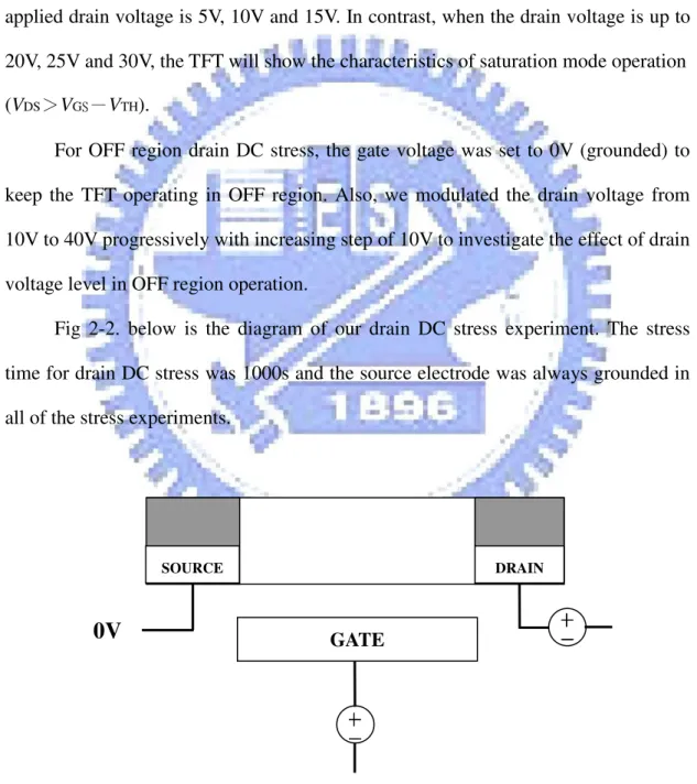
Table 2-1. shows the DC Stress conditions that we designed for our instability testing . For ON region drain DC stress, the gate-bias voltage was set to 20V to keep the TFT channel forming in the a-Si:H layer. Then we modulated the drain voltage from 0V to 30V progressively with increasing step of 5V to investigate the effect of drain voltage level. The typical threshold voltage (VTH) of our a-Si:H TFT sample is about 4V that the TFT shall operate under linear mode (VDS<VGS-VTH) when the applied drain voltage is 5V, 10V and 15V. In contrast, when the drain voltage is up to 20V, 25V and 30V, the TFT will show the characteristics of saturation mode operation (VDS>VGS-VTH).
For OFF region drain DC stress, the gate voltage was set to 0V (grounded) to keep the TFT operating in OFF region. Also, we modulated the drain voltage from 10V to 40V progressively with increasing step of 10V to investigate the effect of drain voltage level in OFF region operation.
Fig 2-2. below is the diagram of our drain DC stress experiment. The stress time for drain DC stress was 1000s and the source electrode was always grounded in all of the stress experiments.
Fig. 2-2. TFT under drain DC stress with gate bias and source grounded.
GATE
0V
-15V
DRAIN SOURCE + - + -+- + - + - + -+- + -17
2.3.2 Drain AC Stress
The basic parameters of AC signal consists of frequency (F), signal peak level (VPEAK), signal base level (VBASE), pulse width (WP), pulse period (T), rising time (TR), and falling time (TF). Fig 2-3 shows the waveform of the AC signal. In AC signal, the definition of individual parameter is given as follows:
F = 1/T (2.2) Duty ratio = WP/T (2.3)
Fig. 2-3. Waveform and definition of the AC signal.
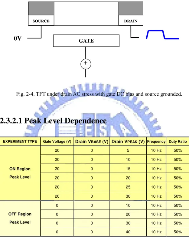
In the drain AC stress experiments, pulse voltage was applied to the drain electrode with gate DC bias while source was grounded, as shown in Fig 2-4. Various experiments for discussing peak level dependence, frequency dependence and duty ratio dependence were performed to verify the mechanism of degradation under drain AC stress. The stress time for drain AC stress was also 1000s.
V
PEAK TR TF 90% 10%V
BASE Pulse Width (WP) Pulse Period (T) Voltage (V) Time (s)18
Fig. 2-4. TFT under drain AC stress with gate DC bias and source grounded.
2.3.2.1 Peak Level Dependence
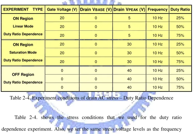
EXPERIMENT TYPE Gate Voltage (V) Drain VBASE (V) Drain VPEAK (V) Frequency Duty Ratio
20 0 5 10 Hz 50% 20 0 10 10 Hz 50% 20 0 15 10 Hz 50% 20 0 20 10 Hz 50% 20 0 25 10 Hz 50% ON Region Peak Level 20 0 30 10 Hz 50% 0 0 10 10 Hz 50% 0 0 20 10 Hz 50% 0 0 30 10 Hz 50% OFF Region Peak Level 0 0 40 10 Hz 50%
Table 2-2. Experiment conditions of drain AC stress - Peak Level Dependence.
Table 2-2. shows the stress conditions that we set for investigating the effect of drain AC peak level. The standard frequency was 10Hz with 50% duty ratio. Gate bias of 0V and 20V also been introduced to keep the TFT operating in OFF region and ON region respectively. For ON region experiment, same as DC stress conditions, the
GATE
0V
-15V
DRAIN SOURCE + - + - + - + -19
drain AC peak level was modulated from 5V to 30V progressively with 5V increasing step. Linear mode operation and saturation mode had been completely contained in the experiment. For OFF region experiment, the drain AC peak level was set to be 10V to 40V progressively with 10V increasing step. Drain base voltage was 0V in all the AC stress experiment.
2.3.2.2 Frequency Dependence
EXPERIMENT TYPE Gate Voltage (V) Drain VBASE (V) Drain VPEAK (V) Frequency Duty Ratio
20 0 5 1 Hz 50% 20 0 5 10 Hz 50% 20 0 5 100 Hz 50% ON Region Linear Mode Frequency Dependence 20 0 5 10000 Hz 50% 20 0 30 1 Hz 50% 20 0 30 10 Hz 50% 20 0 30 100 Hz 50% ON Region Saturation Mode Frequency Dependence 20 0 30 10000 Hz 50% 0 0 40 0.5 Hz 50% 0 0 40 1 Hz 50% 0 0 40 10 Hz 50% 0 0 40 100 Hz 50% 0 0 40 1000 Hz 50% 0 0 40 10000 Hz 50% OFF Region Frequency Dependence 0 0 40 100000 Hz 50%
Table 2-3. Experiment conditions of drain AC stress - Frequency Dependence.
Table 2-3. shows the stress conditions that we set for the frequency dependence experiment. Three different experiment types were listed in the table. In ON region linear mode, the gate bias was 20V with drain peak voltage 5V and base voltage 0V. In ON region saturation mode, the gate bias remained 20V with drain peak voltage
20
changed to 30V and base voltage kept 0V. In OFF region experiment, the gate electrode was grounded to eliminate the channel in a-Si:H layer. The drain peak voltage was 40V and base voltage remained 0V. We changed various frequencies of the drain AC signals that we described upon to investigate the frequency effect of drain AC stress with the standard duty ratio of 50%.
2.3.2.3 Duty Ratio Dependence
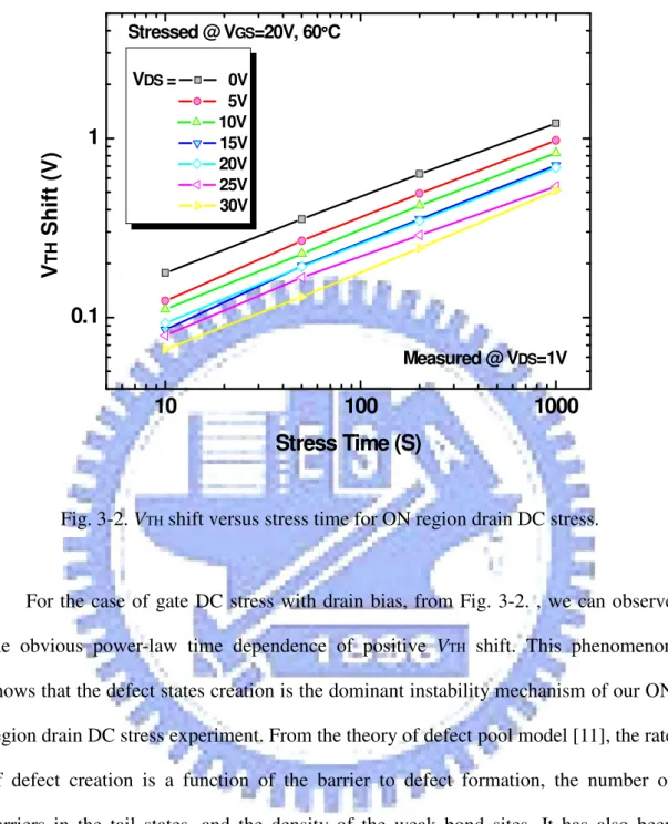
EXPERIMENT TYPE Gate Voltage (V) Drain VBASE (V) Drain VPEAK (V) Frequency Duty Ratio
20 0 5 10 Hz 25%
20 0 5 10 Hz 50%
ON Region Linear Mode
Duty Ratio Dependence 20 0 5 10 Hz 75%
20 0 30 10 Hz 25%
20 0 30 10 Hz 50%
ON Region Saturation Mode
Duty Ratio Dependence 20 0 30 10 Hz 75%
0 0 40 10 Hz 25%
0 0 40 10 Hz 50%
OFF Region Duty Ratio Dependence
0 0 40 10 Hz 75%
Table 2-4. Experiment conditions of drain AC stress – Duty Ratio Dependence
Table 2-4. shows the stress conditions that we used for the duty ratio dependence experiment. Also, we set the same stress voltage levels as the frequency dependence experiment for the three operation modes and chose 10Hz as the standard frequency. But in duty ratio experiment, we changed various duty ratios of drain AC signal to investigate the effect of duty ratio and would try to find out the relationship of effective stress time.
21
Chapter 3
Degradation under Drain DC Stress
3.1 Degradation under Drain DC Stress in On Region
For ON region drain DC stress, the gate-bias voltage was set to 20V to keep the
TFT channel forming in the a-Si:H layer. Then we modulated the drain voltage from 0V to 30V progressively with increasing step of 5V to investigate the effect of drain voltage level. The source electrode was grounded as shown in Fig. 2-2.
3.1.1 Voltage Level Dependence
Fig. 3-1(a) shows the ID-VG transfer curves of the a-Si:H TFTs before and after 1000s of drain DC stress with different drain voltages and 20V gate DC bias. It is observed that threshold voltage (VTH) seriously depends on the supplied drain voltage levels. It is also observed for the sub-threshold swing (SS.). The VTH shift is about +1.2V after 1000s of +20V gate stress without any drain bias. With the increasing of drain bias voltage, the VTH shift decreases obviously and declines to +0.5V when the drain bias increases to +30V, as shown in Fig. 3-1(b). For sub-threshold swing, although the change is not obvious, we can still find its dependence on the drain bias voltage, as shown in Fig. 3-1(c). The SS. changes +0.07 V/Dec under +20V gate stress with no drain bias and decreases to +0.03 V/Dec as the applied drain bias increases to +30V.
22 -2 0 2 4 6 8 1E-11 1E-10 1E-9 1E-8 1E-7 Measured @ VDS= 1V , 60ºC Stress Condition : VGS=20V_DC @ 60ºC, 1000s I D ( A ) VG (V) INITIAL VDS= 0V VDS= 5V VDS=10V VDS=15V VDS=20V VDS=25V VDS=30V
Fig. 3-1(a). ON region VDS dependence of ID-VG degradation.
0 5 10 15 20 25 30 0.2 0.4 0.6 0.8 1.0 1.2 1.4 Measured @ VDS=1V Stressed @ VGS=20V, 60°°°°C, 1000s V T H S h if t (V ) VDS (V)
23 0 5 10 15 20 25 30 0.02 0.04 0.06 0.08 Stressed @ VGS=20V, 60°°°°C, 1000s Measured @ VDS=1V S S . C h a n g e ( V /D e c ) VDS (V)
Fig. 3-1(c). ON region VDS dependence of SS. Change.
From previous reports [8-13], the most important instability mechanisms for a-Si:H TFTs under prolonged gate stress are charge trapping and defect creation. The degradation behavior is usually identified as the combination of both effects. For positive gate DC stress with drain and source grounded, the transfer curves of a-Si:H TFTs show an obvious positive shift with little distortion of the sub-threshold characteristics. The dominant mechanism is defect states creation in the band gap of the a-Si:H layer under lower positive gate bias stress which will increase the threshold voltage with the exhibition of power-law time dependence phenomenon. Little sub-threshold swing change will also been observed. For higher voltage of positive gate bias stress, charge (electrons) trapping in SiNx insulator will take over and increase the threshold voltage more dramatically with logarithmic time dependence.
24
10
100
1000
0.1
1
Measured @ VDS=1V Stressed @ VGS=20V, 60°°°°CV
T HS
h
if
t
(V
)
Stress Time (S)
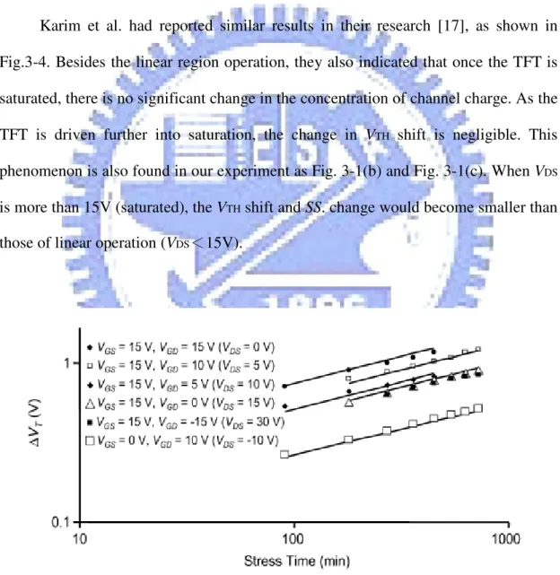
VDS = 0V 5V 10V 15V 20V 25V 30VFig. 3-2. VTH shift versus stress time for ON region drain DC stress.
For the case of gate DC stress with drain bias, from Fig. 3-2. , we can observe the obvious power-law time dependence of positive VTH shift. This phenomenon shows that the defect states creation is the dominant instability mechanism of our ON region drain DC stress experiment. From the theory of defect pool model [11], the rate of defect creation is a function of the barrier to defect formation, the number of carriers in the tail states, and the density of the weak bond sites. It has also been proven that the higher gate bias, the more serious the degradation in a-Si:H TFTs [12]. Back to our experiment, as Fig. 3-3. illustrates, when the drain bias increases, the relative VGD is decreased while VGS remains unchanged. And the carrier concentration in the channel near the drain terminal should be reduced by the decreasing VGD which results in less defect creation. This can explain the drain voltage dependence of a-Si:H TFTs degradation.
25
Fig. 3-3. ON region drain DC stress. (As the drain bias increases, the relative VGD is decreased while VGS remains unchanged.)
Karim et al. had reported similar results in their research [17], as shown in Fig.3-4. Besides the linear region operation, they also indicated that once the TFT is saturated, there is no significant change in the concentration of channel charge. As the TFT is driven further into saturation, the change in VTH shift is negligible. This phenomenon is also found in our experiment as Fig. 3-1(b) and Fig. 3-1(c). When VDS is more than 15V (saturated), the VTH shift and SS. change would become smaller than those of linear operation (VDS<15V).
Fig. 3-4. Dependence of ∆VT on VGS and VGD from the report of Karim et al.
[IEEE ELECTRON DEVICE LETTERS, Vol. 25, No. 4, April 2004.]
D
20V 0VS
10V 20V 10VD
20V 0VS
20V 20V 0VG
G
D
20V 0VS
20V 20VG
26
3.1.2 Damage Region Confirmation
Unlike purely gate stress condition, drain stress is supposed to have asymmetry characteristics because the stress condition is not symmetric between drain and source electrode. To clarify the location of damaged regions in the TFT after drain ON region DC stress, ID-VG transfer curve measurements with forward and reverse mode were performed.
Fig. 3-5(a) shows the I-V curves of ON region before and after 5 V drain DC stress with forward and reverse measurements with VDS=10V. The degradation of forward measurement is worse than that measured with source/drain reversed. The extracted VTH shift which can help us to identify that more obviously is shown in Fig. 3-5(b). For higher drain voltage (30V), this phenomenon is even more apparent, as shown in Fig. 3-6(a) and (b).
-2 0 2 4 6 1E-11 1E-10 1E-9 1E-8 Measured @ VDS=10V Stress Condition : VGS=20V_DC VDS= 5V_DC @ 60°°°°C,1000s I D ( A ) VG (V) 0s 1000s-Forward 1000s-Reverse
Fig. 3-5(a). I-V curve of ON region 5V drain DC stress with forward and reverse measurement under VDS=10V.
27 1 10 100 1000 0.0 0.2 0.4 0.6 0.8 1.0 Measured @ VDS =10V V T H S h if t (V ) Stress Time (S) Forward Reverse Stress Condition : VGS= 20 V_DC VDS = 5 V_DC @ 60°°°°C , 1000s
Fig. 3-5(b). VTH shift versus stress time of ON region 5V drain DC stress with forward and reverse measurement under VDS=10V.
-2 0 2 4 6 1E-11 1E-10 1E-9 1E-8 Measured @ VDS=10V Stress Condition : VGS=20V_DC VDS=30V_DC @ 60°°°°C,1000s I D ( A ) VG (V) 0s 1000s-Forward 1000s-Reverse
Fig. 3-6(a). I-V curve of ON region 30V drain DC stress with forward and reverse measurement under VDS=10V.
28 1 10 100 1000 0.0 0.2 0.4 0.6 Measured @ VDS =10V V T H S h if t (V ) Stress Time (S) Forward Reverse Stress Condition : VGS = 20 V_DC VDS = 30 V_DC @ 60°°°°C , 1000s
Fig. 3-6(b). VTH shift versus stress time of ON region 30V drain DC stress with forward and reverse measurement under VDS=10V.
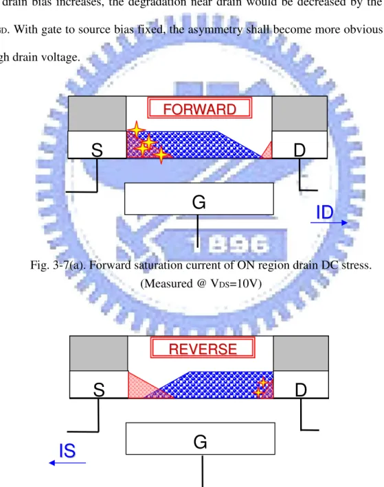
For the forward measurement in the saturation region (VDS >VGS-VTH), there would be a pinch off region formed near the drain electrode. With the increasing drain voltage, this depletion region will increasingly expand toward to the source. Carriers are swept into the drain by the electrical field when they enter this depletion region. Note that the carriers moving into pinch-off region are no longer restricted in the induced channel near the surface, but begin to move away the surface into the bulk. Carriers would have the ability to avoid impacting the high-resistivity region at the SiNx/a-Si:H interface near the drain, even if the region is damaged.
In the condition of our ON region drain DC stress, the source electrode suffers +20V stress from gate bias while the drain suffers lower than that. The drain bias reduces relative VGD and makes the degradation near the drain slighter than near the source. When performing forward current measurement, the induced channel would
29
contain the serious damage region near the source while the slighter damage region would be in the pinch-off region near the drain, as shown in Fig. 3-7(a). In contrast, as Fig. 3-7(b) illustrates, when performing reverse current measurement, the induced channel covers only the slighter damage region near drain while the serious damage region near source would not affect the current effectively. This is the reason why the forward measurement shows more degradation than that of reverse measurement. And as drain bias increases, the degradation near drain would be decreased by the lower VGD. With gate to source bias fixed, the asymmetry shall become more obvious under high drain voltage.
Fig. 3-7(a). Forward saturation current of ON region drain DC stress. (Measured @ VDS=10V)
Fig. 3-7(b). Reverse saturation current of ON region drain DC stress. (Measured @ VDS=10V)
G
D
S
F
F
O
O
R
R
W
W
A
A
R
R
D
D
I
I
D
D
G
S
R
R
E
E
V
V
E
E
R
R
S
S
E
E
D
I
I
S
S
30
3.2 Degradation under Drain DC Stress in OFF Region
For OFF region drain DC stress, the gate and source voltages were set to 0V (grounded) to keep the TFT operating in OFF region. Also, we modulated the drain voltage from 10V to 40V progressively with increasing step of 10V to investigate the effect of drain voltage level in OFF region operation.
3.2.1 Voltage Level Dependence
Fig. 3-8(a) shows the ID-VG transfer curves of the a-Si:H TFTs before and after 1000s of drain DC stress in OFF region with variant drain voltages . The I-V curves have obvious negative shifts with little sub-threshold swing (SS.) change and are drain voltages dependent. From the extracted data in Fig. 3-8(b), the VTH shift is about -0.15V after 1000s of +10V drain DC stress in OFF region and increases to -0.8V as the drain voltage is up to +40V. For sub-threshold swing, the degradation is even less than in ON region stress, but it still depends on the drain bias, as shown in Fig. 3-8(c).
-2 0 2 4 6 1E-11 1E-10 1E-9 1E-8 1E-7 Measured @ VDS= 1V Stress Condition : VGS=0V @ 60ºC, 1000s I D ( A ) VG (V) INITIAL VDS= 10V VDS= 20V VDS= 30V VDS= 40V
31 10 20 30 40 -1.0 -0.8 -0.6 -0.4 -0.2 0.0 Measured @ VDS=1V Stressed @ VGS=0V, 60°°°°C, 1000s V T H S h if t (V ) VDS (V)
Fig. 3-8(b). OFF region VDS dependence of VTH Shift.
10 20 30 40 -0.04 -0.02 0.00 0.02 0.04 Measured @ VDS=1V Stressed @ VGS=20V, 60°°°°C, 1000s S S . C h a n g e ( V /d e c ) VDS (V)
32
As we can see, the I-V curves show significant similarity between OFF region drain DC stress and negative gate DC stress. For negative gate DC stress, it has been reported that the transfer curves would have negative shifts with little sub-threshold swing change, as shown in Fig. 1-1. [15]. Defect removal below the Fermi level would take over the defect creation and become the dominant mechanism [14] with the exhibition of power-law time dependence. Positive carriers (holes) would also be trapped in the silicon-nitride insulator under sufficiently high negative gate stress.
10
100
1000
0.01
0.1
1
10
Stressed @ VGS=0V, 60°°°°C Measured @ VDS=1V V
T HS
h
if
t
(
V
)
Stress Time (S)
VDS= 10 V 20 V 30 V 40 VFig.3-9. Absolute value of VTH shift versus stress time for OFF region drain DC stress.
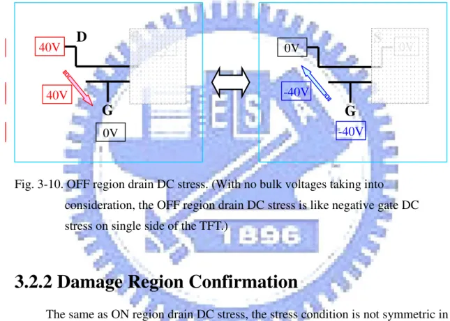
Regardless of the polarity, Fig. 3-9. shows the relationship between the absolute value of the VTH shift and stress time. It is obvious that the power-law time dependence also appears in our OFF region drain DC stress experiment. This should be the evidence of defect removal dominance. With no bulk voltages should be taken
33
into consideration, the OFF region drain DC stress is just like the stress condition of negative gate DC stress on single side of the TFT, as illustrated in Fig. 3-10. That is the reason why the I-V degradation behavior of OFF region drain DC stress is extremely similar to negative gate DC stress. As the drain bias increases, the relative VGD becomes more negative and introduces more degradation. This can finely explain the drain voltage dependence in OFF region.
Fig. 3-10. OFF region drain DC stress. (With no bulk voltages taking into
consideration, the OFF region drain DC stress is like negative gate DC stress on single side of the TFT.)
3.2.2 Damage Region Confirmation
The same as ON region drain DC stress, the stress condition is not symmetric in OFF region experiment. The degradation of OFF region drain DC stress is supposed to also have asymmetry between source and drain electrodes.
Fig. 3-11(a) is the I-V curves of OFF region before and after 40V drain DC stress with forward and reverse measurements under saturation mode (VDS=10V). The degradation of reverse measurement is obviously worse than that of forward measurement. The extracted VTH shift in Fig. 3-11(b) presents the difference between forward and reverse more certainly.
0V
S
G
D
0V 40V 40VS
0V -40V 0V -40VG
34 -4 -2 0 2 4 1E-11 1E-10 1E-9 Measured @ VDS=10V Stress Condition : VGS= 0V_DC VDS= 40V_DC @ 60°°°°C,1000s I D ( A ) VG (V) 0s 1000s-Forward 1000s-Reverse
Fig. 3-11(a). I-V curve of OFF region drain DC stress with forward and reverse measurement under VDS=10V. 1 10 100 1000 -1.0 -0.8 -0.6 -0.4 -0.2 0.0 0.2 Measured @ VDS =10V V T H S h if t (V ) Stress Time (S) Forward Reverse Stress Condition : VGS= 0 V_DC VDS = 40 V_DC @ 60°°°°C , 1000s
Fig. 3-11(b). VTH shift versus stress time of OFF region drain DC stress with forward and reverse measurement under VDS=10V.
35
In the condition of OFF region drain DC stress, the bias voltage is applied to the drain electrode only. With no electric field between source and gate, the degradation would be confined near the drain electrode. When we perform forward current measurement, the serious damage region near the drain would be located in the pinch-off region instead of be covered with the induced channel, as shown in Fig. 3-12(a). In contrast, as Fig. 3-12(b) illustrates, when performing reverse current measurement, the induced channel would contain the damage region near drain and seriously affect the current transfer. So we see more degradation in reverse measurement than in forward measurement.
Fig. 3-12(a). Forward saturation current of OFF region drain DC stress. (Measured @ VDS=10V)
Fig. 3-12(b). Reverse saturation current of OFF region drain DC stress. (Measured @ VDS=10V)
G
D
S
F
F
O
O
R
R
W
W
A
A
R
R
D
D
I
I
D
D
G
S
R
R
E
E
V
V
E
E
R
R
S
S
E
E
D
I
I
S
S
36
Another phenomenon of the asymmetry will occur if we compare the forward I-V curves measured with linear mode (VDS=1V) and saturation mode (VDS=10V). Fig. 3-13(a) shows the forward I-V curves of OFF region before and after 40V drain DC stress with linear and saturation mode measurements. The negative transfer curve shift of linear measurements (ID1) is more obvious than that of saturation measurements (ID2) and almost catches up on the initial offset between them. The extracted VTH shift in Fig. 3-13(b) can help us to observe the difference more clearly. Similar to the forward and reverse measurements, the reason of causing the difference would be the location of damage region. For linear measurement, there is no pinch-off region in the channel that the damage region near the drain terminal would seriously degrade the transfer curve. On the other hand, for saturation measurement, there should be a pinch-off region formed near the drain. The damage region will not be fully contained in the channel that will cause less degradation. So we can see the difference between linear and saturation measurements.
37 0 2 4 1E-10 1E-9 Stress Condition : VGS= 0V_DC VDS= 40V_DC @ 60°°°°C,1000s ID1 Measured @ Vds= 1V ID2 Measured @ Vds=10V I D ( A ) VG (V) ID1-0s ID2-0s ID1-1000s ID2-1000s
Fig. 3-13(a). I-V curve of OFF region drain DC stress with linear mode (VDS=1V) and saturation (VDS=10V) mode measurement.
1 10 100 1000 -1.0 -0.8 -0.6 -0.4 -0.2 0.0 0.2 V T H S h if t (V ) Stress Time (S) Linear Mode (Measured @ VDS = 1V) Saturation Mode (Measured @ VDS =10V) Stress Condition : VGS= 0 V_DC VDS = 40 V_DC @ 60°°°°C , 1000s
Fig. 3-13(b). VTH shift versus stress time of OFF region drain DC stress with linear mode (VDS=1V) and saturation mode (VDS=10V) measurement.