國 立 交 通 大 學
電子工程學系 電子研究所
博 士 論 文
橫向擴散的射頻金氧半場效電晶體之佈局設計與
熱特性分析
Layout Design and Thermal Characterizations of RF
LDMOS
研 究 生 :胡 心 卉
指導教授 :張 俊 彥 院 士
陳 坤 明 博 士
橫向擴散的射頻金氧半場效電晶體之佈局設
計與熱特性分析
Layout Design and Thermal Characterizations of RF
LDMOS
研 究 生 :胡 心 卉
Student: Hsin-Hui Hu
指導教授 :張 俊 彥 院 士
Advisor: Dr. Chun-Yen Chang
陳 坤 明 博 士
Dr. Kun-Ming Chen
國 立 交 通 大 學
電子工程學系 電子研究所
博 士 論 文
A Dissertation
Submitted to Department of Electronics Engineering and
Institute of Electronics
College of Electrical and Computer Engineering
National Chiao Tung University
In Partial Fulfillment of the Requirements
For the Degree of
Doctor of Philosophy
in
Electronics Engineering
September 2008
Hsinchu, Taiwan, Republic of China
中華民國九十七年九月
橫向擴散的射頻金氧半場效電晶體之佈局設計與熱特性分析
研究生: 胡 心 卉
指導教授: 張 俊 彥 院士
陳 坤 明 博士
國立交通大學
電子工程學系 電子研究所博士班
中文摘要
近年來,射頻橫向擴散金氧半場效電晶體(RF LDMOS)已廣泛地應用在
手機基地台中,作為功率放大器的主要元件。為了能因應新一代通訊標準
的需求,LDMOS 的特性必須不斷的加以改進。在本論文中,我們將探討兩
種結構:ring 和 fishbone 的直流、高頻和射頻功率特性。在 fishbone 結構
中,我們設計了具有不同漂移(drift)區長度、閘極長度、閘極指根數目與結
構單元數目的元件。其中,具有較短漂移區長度的元件雖有較小的崩潰電
壓,但其直流、高頻特性以及線性度均比較長漂移區長度的元件來的好。
為了得到較低的開啟態電阻(on-resistance)以及緊密的排列結構,我們採用
了一種四邊形的 ring 結構。在傳統的 MOSFET 中,寄生汲極電容指的是 n
+的汲極和 p 型基底間的接面電容。因此,汲極通常擺在內側來降低寄生電
容。而在 LDMOS 的元件中,寄生電容指的是 deep n-well (DNW)和 p 型基
底間的接面電容。所以汲極擺在外側的結構並不會提高汲極電容。再者,
由於 ring 結構排列較 fishbone 緊密,使得 DNW 的面積減小,汲極電容降
低。為了能更進一步了解元件參數對高頻特性的影響,我們以小訊號等效
電路將其參數萃出作為分析比較。實驗結果顯示,ring 結構之所以有較佳的
特性是由於其寄生的汲極電阻比 fishbone 來的小。在 ring 結構中,汲極擺
在閘極外側能有效的增加汲極面積,降低汲極電阻,進而達到降低元件開
啟態電阻的目的。我們所設計的 ring 結構可以在相同的崩潰電壓基礎下降
低開啟態電阻,並將最大震盪頻率(f
max) 提升 24.5%。此外輸出功率、功率
增益以及附加功率效率均有較佳的表現,而線性度則和 fishbone 結構不相
上下。由於 ring 結構只更動光罩之設計,製程流程並無改變,因此實為一
大優點。
由於功率元件深受溫度的影響,因此元件的溫度效應也將一並討論。
由之前的實驗結果得知,LDMOS 有較大的的寄生汲極電阻。因此需扣除寄
生電阻的影響才能得到正確的溫度引起之 f
T變化對轉導變化的關係。ring
結構由於排列較的較緊密,因此有較大的熱阻和較小的熱容,也就是自我
熱效應比 fishbone 嚴重。在脈衝量測下,不論直流還是高頻特性均顯示 ring
有較好的特性。因此若是在脈衝模式操作下,ring 結構將會有更佳的特性表
現。
另一方面,元件的電容特性也有完整的分析。由於 LDMOS 的通道為
非均勻參雜且具有漂移區,因此電容會有峰值產生。而在較大的汲極偏壓
下,我們首次發現 ring 結構的電容會出現第二個峰值。這是因為 ring 結構
的轉角處電流密度較小,使得閘極需偏壓在較大的電壓下才會進入類飽
和。藉由溫度的變化來研究電容的改變,我們發現電容主要是受到臨限電
壓、類飽和電流和漂移區的空乏電容所影響。因此在建立電容模型時,必
須將這些效應考慮進去,以提升模擬的準確度。此外,根據實驗的結果來
選擇電容對溫度較不敏感的偏壓區域對於電路的設計也極為重要。
Layout Design and Thermal Characterizations of RF LDMOS
Student: Hsin-Hui Hu Advisors: Dr. Chun-Yen Chang
Dr. Kun-Ming Chen
A Dissertation
Department of Electronics Engineering and Institute of Electronics
National Chiao Tung University, Hsinchu, Taiwan
Abstract
RF LDMOS is nowadays widely used for base station applications. To meet the demands imposed by new communication standards, the performance of LDMOS is subject to continuous improvements. In this thesis, two types of layout structures, ring and fishbone, were studied for DC, high-frequency, and RF power characteristics. For fishbone structures, variation of drift lengths and channel widths, different numbers of gate fingers and cells were investigated. The structure with smaller LDrift has better on-resistance, fT, fmax, and linearity, but smaller breakdown voltage. To achieve lower on-resistance and a more compact device size, we adopted a “ring” structure in the layout design. In the traditional design, drain inside was usually used to lower the parasitic drain capacitance. For MOSFET, the conventional parasitic drain capacitance refers to the n+ drain to p-substrate junction capacitance. Hence, the drain was always surrounded by the transistor channel and source to reduce the area. In LDMOS, however, the parasitic drain capacitance refers to the deep n-well (DNW) to p-substrate junction capacitance. Therefore, drain capacitance would not increase in a drain outside structure. Since the ring has more compact device size the area of DNW is smaller than the fishbone. This smaller area leads to a lower drain capacitance in the ring structure. In
order to determine the effect of device parameters on high-frequency characteristics more clearly, small-signal equivalent circuit was built to be analyzed. From the simulation results, the smaller drain parasitic resistance in the ring could be the key factor for improving fT and
fmax. For having the drift region, drain parasitic resistance is larger in the LDMOS than in the MOSFET and become an important parameter. In the ring structure, drain outside design has an advantage over drain inside in having larger area for output terminal. The extra areas in the corner would have lowered the drain parasitic resistance and improve the on-resistance. By using the ring structure, higher drain current and transconductance were shown by the reason of larger equivalent W/L and lower drain parasitic resistance. Also, fmax were enhanced by about 24.5% due to the lower drain parasitic resistance. As for microwave power characteristics, output power, power gain and power added efficiency (PAE) were improved with a similar linearity compared to the fishbone. Its reveals that the ring structure had a better performance and similar breakdown voltage compared to the fishbone structure, without altering the process flow.
For high-power applications, temperature is an important issue. For conventional MOS transistors in RF applications, the temperature effect was investigated by studying the temperature dependence of fT, which is proportional to the transconductance. Owing to the higher drain resistance in the LDMOS transistors, the fT is also affected by drain resistance. By de-embedding the effect of drain resistance, we show the real relation between the temperature-induced variation of fT and transconductance. In order to study the self-heating effect on the performance of LDMOS, I-V and RF characteristics were also measured under a pulsed condition. From the extracted thermal resistance and thermal capacitance, the effect of self-heating was more severe in ring structure. In the pulsed-mode measurement, the ring has better drain current, fT and fmax than the fishbone structure. Although the ring structure showed lower static drain current than the fishbone structure at high gate biases due to the significant self-heating effect, its current drive capability could be improved using a pulsed-mode
operation.
In another part of this thesis, we discussed and analyzed the capacitance characteristics completely. For having a non-uniform doping channel and the existence of the drift region, CGS+ CGB and CGD exhibit a peak in LDMOS. In the ring structure, the second peaks in a capacitance-voltage curve have been observed at high drain voltages for the first time. While the corner region of the drift in the ring shows lower current density than the edge region, it needs higher gate voltage to enter quasi-saturation. By increasing the gate voltage, the current in the corner region is high enough to make the velocity of electrons in the drift saturated. Therefore, the corner operates in quasi-saturation and second peaks are generated. The thermal effects on capacitances were also investigated. Because the capacitances are affected mainly by the threshold voltage, quasi-saturation current and drift depletion capacitance, the variation of the capacitances with temperature is more complicated than that in conventional MOSFET, and it depends on the bias condition. Based on the result we analyzed, we can well model the temperature-dependence capacitance by adding these parameters and also can choose a bias condition with lower temperature sensitivity in capacitances.
誌 謝
在四年的博士班生活中,感謝我的指導教授張俊彥院士,在繁忙的校
務工作之餘仍耐心地給予我們學術上的指導和鼓勵。在卸下校長一職之
後,依然醉心於研究。老師對於學術的熱誠深深地影響我們做學問的態度。
感謝國家奈米元件實驗室研究員陳坤明博士和黃國威博士在研究上經驗的
傳承,並在實驗的過程中不厭其煩的幫助我克服許多困難。對於兩位學長
給予我的支持與協助,由衷的感謝。
感謝 NDL 高頻元件實驗室的工程師王生圳學長和邱佳松學長在量測上
的幫助,祝福你們順利取得博士學位。也謝謝文林學長、國祥、柏源、書
毓和汶德在儀器方面的鼎力相助。對於大部分時間都在高頻實驗室做實驗
的我,非常感謝大夥們陪我度過了那段埋首實驗的苦澀時光。
感謝 CYC 實驗室畢業的陳漢譽博士和黃聖懿博士不論在課業、實驗以
及生活上都給予莫大的幫助,即使學長畢業了,依然熱心地提供建議,幫
忙解決問題。同時也謝謝實驗室畢業的吳永俊博士、李宗霖博士、凃俊豪
博士、楊宗熹博士,與實驗室的怡誠、兆欽、立偉、緯仁、勝杰、誌陽、
哲榮和貴宇,還有助理小姐伊喬、秋梅以及所有 CYC 的成員們,謝謝你們
在這段時間的相伴,讓我的研究生活增添了許多歡樂與豐富的色彩。另外
也感謝在新竹的姊妹們祥梅、婉棋、阿吉和靜芬,不論是談心、一起聚餐
還是看電影,多虧了妳們的陪伴,讓我留下了許多美好的回憶。
最後要感謝親愛的爸爸、媽媽,感謝你們長久以來對我無限的支持、
關愛及包容,由於你們的付出與鼓勵讓我後顧之憂,我今天的所有,都是
你們犧牲一切所換來的。雖然一想到這些就不忍落淚,但是我知道,拿到
學位是對你們最大報答。很高興地,我做到了。今後,該換我為你們付出
了。
胡心卉
於 新竹交通大學
二零零八年九月 秋
Contents
Chinese Abstract
i
English Abstract
iv
Acknowledgement
vii
Contents
ix
Table Captions
xii
Figure Captions
xiii
Chapter 1 Introduction
1.1
Introduction
to
RF
LDMOS
1
1.1.1 Advantages Compared to the Bipolar Technology
2
1.1.2 Advantages Compared to Other Materials
2
1.2 Motivation
3
1.3 Thesis Organization
4
Reference
6
Chapter 2 Characterization of RF LDMOS with Different Layout Design
2.1 Introduction
9
2.2 RF
LDMOS
with
Fishbone
Structure
9
2.2.1 DC Characteristics
10
2.2.2 High-frequency Characteristics
11
2.3 Comparison of Two Layout Design: Fishbone and Ring
13
2.3.1 DC Characteristics
13
2.3.2 High-frequency Characteristics
14
2.4 Summary
17
Reference
19
Chapter 3 Thermal Effects on DC and RF Performances of RF LDMOS
3.1 Introduction
43
3.2 Characteristics of RF LDMOS at various Temperatures
43
3.2.1 DC Characteristics
44
3.2.2 High-frequency Performance
45
3.2.3 S-parameters Characteristics
47
3.3 Pulsed I-V/RF Characteristics of RF LDMOS
48
3.4 Summary
50
Reference
52
Chapter 4 Thermal Effects on Capacitance Characteristics of RF LDMOS
4.1
Introduction 70
4.2 Capacitances versus V
GS70
4.3 Capacitances versus V
DS73
4.4 Thermal Effect on Capacitances versus
Gate
Voltage
73
4.5 Thermal Effect on Capacitances versus
Drain
Voltage
75
4.6 Summary
76
Reference
78
Chapter 5 Conclusion and Suggestion for Future Work
5.1 Conclusion
91
Table Captions
Chapter 2
Table 2-1 The extracted on-resistances for three samples with various drift lengths. 22 Table 2-2 Cut-off frequency and maximum oscillation frequency for three samples 22
with various drift lengths.
Table 2-3 Extracted gm, Rd, Cgd, and Cgs for fishbone structure with various drift 23 lengths. The fT and fmax differences between the LDrift=3.6μm and
3.0μm due to the change of model parameters are also listed.
Table2-4 Extracted gm, Rd, Cgd, Cgs, and Cjdb for different layout structures. 23 The fT differences between the fishbone and ring structures due to the change of model parameters are also listed.
Table 2-5 Extracted Rd, Cjdb, and Rg for different layout structures. The fmax 24 differences between the fishbone and ring structures due to the change of model parameters are also listed.
Figure Captions
Chapter 2
Fig.2-1 LDMOS layout structures: (a) fishbone and (b) ring. 25 Fig.2-2 Schematic cross section of an LDMOS transistor. 26 Fig.2-3 Fishbone layout structures: (a) Sample 1 and (b) Sample 3. 27 Fig.2-4 (a) Subthreshold and (b) output characteristics of LDMOS transistors 28
with different drift lengths.
Fig.2-5 Dependence of (a) |h21| and (b) MSG/MAG on frequency obtained 29 from S-parameter measurements.
Fig.2-6 A simple equivalent circuit model of the LDMOS. 30 Fig.2-7 (a) Intrinsic transconductance and (b) Cgs and Cgd versus drift length 31
with different samples.
Fig.2-8 (a) Subthreshold and (b) output characteristics of LDMOS transistors 32 with different layout structures.
Fig.2-9 Ron versus LDriftfor different layout structures. 33 Fig.2-10 Cut-off frequency and maximum oscillation frequency versus the drift 34
length.
Fig.2-11 (a) Effects of small-signal model parameters on fT 35 (b) Effects of small-signal model parameters on fmax. 36 Fig.2-12 Rd versus LDrift for LDMOS with different layout structures. The inset 37
shows that the drain region of the ring structure had extra areas (the shaded regions) compared with the fishbone structure.
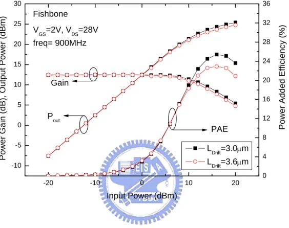
Fig.2-13 Output power, power gain and PAE versus input power with different 38 drift lengths.
Fig.2-14 Drain current versus gate voltage with different drift lengths. The input 39 signal was bias at VGS=2V and the negative duty cycle of output signal was clipped by the cutoff region.
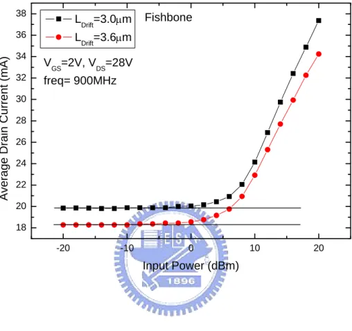
Fig.2-15 Average drain current as a function of the input power with different 40 drift lengths.
Fig.2-16 Output power, power gain and PAE versus input power with different 41 layout structures.
Fig.2-17 Output power and third-order intermodulation power versus input power 42 with different layout structures.
Fig.3-1 (a) Subthreshold and (b) output characteristics of LDMOS transistors 55 with different layout structures at 0 and 50oC.
Fig.3-2 Threshold voltage variation with temperature for different layout structures. 56 Fig.3-3 Temperature dependence of channel mobility for different layout structures. 57 Fig.3-4 Cutoff frequency and maximum oscillation frequency versus gate 58
voltage at various temperatures.
Fig.3-5 Extrinsic and intrinsic transconductances versus gate voltage at 59 various temperatures for different layout structures.
Fig.3-6 (a) Extrinsic fT and (b) intrinsic fT variations versus intrinsic 60 transconductance variation when temperature changes from 25oC.
Fig.3-7 Extrinsic fmax variation versus intrinsic transconductance variation 61 when temperature changes from 25oC.
Fig.3-8 Measured (open symbols) and simulated (solid line) S-parameters of 62 transistors with (a) fishbone and (b) ring structures from 0.1 to 10 GHz.
Fig.3-9 Measured (open symbols) and simulated (solid line) |S22| of 63 transistors for different layout structures from 0.1 to 10 GHz.
Fig.3-10 Timing diagram showing the relationship of the applied bias, the RF input 64 signal, and the sample points for pulsed measurement.
Fig.3-11 Output characteristics of an LDMOS under static and pulsed conditions. 65 Fig.3-12 Output characteristics of LDMOS transistors with different layout 66
structures under pulsed condition.
Fig.3-13 (a) Cutoff frequency and (b) maximum oscillation frequency versus the 67 gate voltage under cw- and pulsed-mode measurements.
Fig.3-14 Channel temperature versus power dissipation with different layout 68 structures.
Fig.3-15 Thermal transient response with different layout structures. The inset 69 shows the transient drain current for both fishbone and ring.
Chapter 4
Fig.4-1 Extracted CGS+CGB, CGD and the drain current versus gate voltage at 80 different drain biases for the fishbone structure.
Fig.4-2 Simulated CGS+CGB for four test structures: (a) uniform doped channel 81 and without drift region, (b) non-uniform doped channel and without
drift region, (c) uniform doped channel and with drift region, (d) non-uniform doped channel and with drift region.
Fig.4-3 Device configurations (a) without drift region and (b) with drift region 82 when gate voltage exceed the threshold voltage and drain voltage is low.
for the ring structure.
Fig.4-5 Schematic view of layout structure and current distribution: 84 (a) fishbone structure and (b) ring structure.
Fig.4-6 Extracted CGS+CGB and CGD versus drain voltage at different gate biases 85 for the fishbone structure.
Fig.4-7 Extracted CGS+CGB and CGD versus drain voltage at different gate biases 86 for the ring structure.
Fig.4-8 Extracted CGS+CGB and CGD versus gate voltage with various 87 temperatures at drain voltage (a) VDS=0.1 V and (b) VDS=5 V for a
fishbone structure. The inset shows the drain current versus gate voltage with various temperatures.
Fig.4-9 Extracted CGS+CGB and CGD versus gate voltage with various 88 temperatures at drain voltage (a) VDS=0.1 V and (b) VDS=5 V for a ring structure. The inset shows the drain current versus gate voltage with various temperatures.
Fig.4-10 Extracted CGS+CGB and CGD versus drain voltage with various 89 temperatures at (a) VGS=1 V and (b) VGS=2 V for a fishbone structure.
Fig.4-11 Extracted CGS+CGB and CGD versus drain voltage with various 90 temperatures at (a) VGS=1 V and (b) VGS=2 V for a ring structure.
Chapter 1
Introduction
1.1 Introduction to RF LDMOS
The Lateral-Diffused MOS (LDMOS) transistors are traditionally used in switching applications for a high voltage device and enter to the RF power application in the early 70’s. The first publication of LDMOS for microwave operation was demonstrated in 1972 [1]. Until now, LDMOS are used in a wide range of applications requiring RF power amplification like: Wireless infrastructure (GSM, EDGE, WCDMA, and WiMAX); Broadcast; pulsed radar; industrial, scientific and material (ISM) applications; avionics and military application [2]. Up to 2005, Si LDMOS covered about 90 percent of the high power RF amplification applications in the 2GHz and higher frequency range, according to market analyst company Yole Développement. Now, Wireless infrastructure still represents the largest segment for RF power semiconductors. RF power amplifiers are key components in base stations for personal communication systems and require for low cost, high efficiency, and good linearity [3]. For frequencies ranging from 450 MHz to 2.7 GHz, LDMOS transistor technology has played a predominant role in the power amplifier applications due to its advantages in performance, cost, reliability, and power capability [4]. LDMOS process was introduced and targeting the base stations market in the early 1990s [5]. This technology has already gone through a lot of gradual progress so far. The market for base-station power amplifiers in wireless communication systems has grown rapidly in recent years. Silicon based LDMOS have been used for wireless technologies like GSM, EDGE, CDMA, WCDMA and WiMAX [6]. Now, capable of operation at frequency up to 3.5GHz and 3.8GHz for WiMAX are on the market [7-8].
1.1.1 Advantages Compared to the Bipolar Technology
The advantages of using LDMOS for high power high frequency applications are on the following points:
High linearity: the process controlled short channel length makes the device works in velocity
saturation. The linear relation of drain current and gate voltage leads to a constant transconductance and improve the linearity.
Higher gain: the power gain can be improved by the lower source inductance and lower
feedback capacitance. The former can be done by tying the source and P-body together to the RF ground. In bipolar, the backside collector requires insulating from the ground and the top side emitter needs bond wire to connect to the ground. The additional bond wire introduces high inductance and limits the power gain. Also, the LDMOS is a lateral structure device which has lower feedback capacitance compared with a bipolar transistor. In addition, the LDMOS has negative temperature coefficient and does not need ballast resistor which used in bipolar and degrade the bipolar’s power gain. Therefore, the LDMOS provides higher gain than bipolar for the same output power level. This means that less amplifier stages are needed, and thus gives higher reliability and lower cost.
Thermal stability: LDMOS has no thermal runaway problem due to its negative temperature
coefficient. The higher drain current leads to higher temperature which lowers the channel mobility and resulting in a drop in drain current. On the other hand, the temperature coefficient in bipolar is positive and more prone to thermal runaway
High ruggedness: LMODS has positive temperature coefficient of channel resistance and high
drain-source breakdown voltage. Consequently, LDMOS has excellent ruggedness into an output mismatch VSWR typically 10:1 whereas the bipolar can only accept 3:1 [9-10].
1.1.2 Advantages Compared to Other Materials
bandgap materials: SiC and GaN. GaAs based power devices can achieve higher drain efficiency and linearity due to a higher electron mobility and higher saturation velocity then silicon. However, lower thermal conductivity about 0.46 W/cm K limits the applicability of GaAs for the high power final stage amplifiers which is needed in base station transmitters. Also, the conventional GaAs-based FET’s have serious limitations in terms of operation voltage as compared with LDMOS and typically suitable for handset application [11]. The wide bandgap materials, SiC and GaN, have high electric breakdown voltage field and high saturation velocity. However, even a superior technology must be cost competitive. High cost (for the expensive substrate) in comparison to LDMOS and GaAs shows the must significant barrier to market adoption for GaN and SiC [12]. For LDMOS, the high thermal conductivity about 1.5 W/cm K with the drift region design achieve quite high operation voltage which makes this technology suitable for base station power amplifier.
1.2 Motivation
By scaling down the gate length and the drift length, the performance can be significantly improved with lower on-resistance and higher transconductance. However, the scaling may have reached the limit of high-voltage endurance during power-amplifying operations. In the conventional LDMOS, there is a trade-off between the on-resistance and the breakdown voltage; the drain current and the breakdown voltage. Several researchers have proposed solutions to these trade-offs such as using a double-doped offset [13], or a stacked or step drift region [14-16], or even the strain structure [17]. As well as by changing the device process flow, the trade-off between the on-resistance and the breakdown voltage can also be solved by optimizing the layout design. In this thesis, two types of layout structures, ring and fishbone, were studied for DC, high-frequency, and RF power characteristics.
investigated. The cutoff frequency (fT) and maximum oscillation frequency (fmax) are critical figures of merit for evaluating the performance of RF transistors. According to its structure, the parasitic drain resistance of the LDMOS becomes more important than that of the conventional MOSFET for the present drift region. However, in most of the studies, the effect of the parasitic resistance was not considered when analyzing the temperature effect on the device characteristics [18-20]. By de-embedding the effect of the parasitic source and drain resistors from the measured S-parameters, the temperature dependence of the intrinsic fT can be analyzed. Several researchers have investigated the effects of temperature on the reliability and dc performances of LDMOS transistors [21-23]. However, the temperature effects on the high-frequency characteristics of LDMOS have seldom been addressed. In addition, the device capacitances influence the input, output and feedback capacitances, which are important in the dynamic operation, and have large impact on device high-frequency performance. The capacitance characterization and modeling of LDMOS transistors have been studied widely [24-28]. Nevertheless, the temperature effects on the capacitance characteristics of LDMOS transistors are not mentioned in previous literatures. In this thesis, the DC, high-frequency, and RF power characteristics of LDMOS transistors with different layout structures were studied at various temperatures. Also, the temperature effects on capacitance characteristics were analyzed.
1.3 Thesis Organization
The content in this thesis includes the following parts.
Chapter 1 introduces the LDMOS for RF applications and the motivation of this thesis. Chapter 2 presents two layout structures, ring and fishbone. The DC, high-frequency and RF power performance were analyzed with various drift length and channel width. Also, small-signal model parameters were extracted to investigate the effect of different parameters on fT and fmax.
Chapter 3 presents thermal effects on DC and RF performance of RF LDMOS with ring and fishbone structures. By de-embedding the effect of the parasitic source and drain resistors, the temperature dependence of the intrinsic fT can be analyzed. In addition, Pulsed I-V and RF characteristics were measured to investigate the self-heating effect on the performance of an LDMOS.
Chapter 4 presents the unusual behavior in capacitance of RF LDMOS with ring and fishbone structures. The capacitance characteristics have also been studied at various temperature conditions. Both capacitance versus gate voltage with different drain voltage and capacitance versus drain voltage with different gate voltage were investigated.
References
[1] H. J. Sigg, G. D. Vendelin, T. P. Cauge, and J. Kocsis, “D-MOS transistor for microwave applications,” IEEE Trans. Electron Devices, vol. 19, no. 1, pp. 45-53, 1972.
[2] P. Aaen, J. A. Plá, and J. Wood, Modeling and Characterization of RF and Microwave
Power FETs, Cambridge University Press, 2007.
[3] F. van Rijs, and S. J. C. H. Theeuwen, “Efficiency improvement of LDMOS transistors for base stations towards the theoretical limit,” IEDM Tech. Dig., Dec. 2006, pp. 11–13. [4] A. Wood, C. Dragon, and W. Burger, “High performance silicon LDMOS technology for
2GHz RF power amplifier applications,” IEDM Tech. Dig., Dec. 1996, pp. 87–90.
[5] J. Rice, “LDMOS linearity and reliability,” Microwave Journal, Vol. 45, No. 6, June 2002, pp. 64-72.
[6] F. van Rijs, and S. J. C. H. Theeuwen, “Efficiency improvement of LDMOS transistors for base stations: towards the theoretical limit,” IEDM Tech. Dig., Dec. 2006, pp. 205-208. [7] C. Cassan, and P. Gola, “A 3.5 GHz 25 W Silicon LDMOS RFIC power amplifier for
WiMax frequencies,” IEEE RFIC Symposium Digest, pp. 87-90, 2007.
[8] F. van Rijs, “Status and trends of silicon LDMOS base station PA technologies to go beyond 2.5 GHz applications,” in Proc. IEEE Radio and Wireless Conf., 2008, pp.69-72. [9] A. Wood and W. Brakensiek, “Application of RF LDMOS Power Transistor for 2.2 GHz
Wideband-CDMA,” in Proc. IEEE Radio and Wireless Conf., 1998, pp. 309-312.
[10] J. J. Bouny, “Advantages of LDMOS in high power linear amplification,” Microwave
Engineering Europe, April 1996, p. 37–40.
[11] S. McGrath, and T. Rödle, “Moving past the hype: real opportunities for wide band gap compound semiconductors in RF power markets,” in Proc. CS GaAs Mantech, paper. 1.4, April. 2005.
[12] B. Vassilakis, A. Cava, and W. Veitschegger, “Wireless base station technology evolution,” in Proc. IEEE Compound Semiconductor Integrated Circuit Symp., 2004, pp.
3-7.
[13] M. Shindo, M. Morikawa, T. Fujioka, K. Nagura, K. Kurotani, K. Odaira, T. Uchiyama, and I. Yoshida, “High power LDMOS for cellular base station applications,” in Proc.
IEEE SISPAD, 2001, pp. 107-110.
[14] J. Cai, C. Ren, N. Balasubramanian, and J. K. O. Sin, “A novel high performance stacked LDD RF LDMOSFET,” IEEE Electron Device Lett., vol. 22, No. 3, pp. 236-238, May 2001.
[15] S. Xu, P. Foo, J. Wen, Y. Liu, F. Lin, and C. Ren, “RF LDMOS with extreme low parasitic feedback capacitance and high hot-carrier immunity,” IEDM Tech. Dig., Dec. 1999, pp. 201-204.
[16] G. Cao, S. K. Manhas, E. M. Sankara Narayanan, M. M. De Souza, and D. Hinchley, “Comparative study of drift region designs in RF LDMOSFETs,” IEEE Trans. Electron
Devices, vol. 51, no. 8, pp. 1296-1303, August 2004.
[17] M. Kondo, N. Sugii, Y. Hoshino, W. Hirasawa, Y. Kimura, M. Miyamoto, T. Fujioka, S. Kamohara, Y. Kondo, S. Kimura, and I. Yoshida, “High Performance RF Power LDMOSFETs for Cellular Handsets Formed in Thick-Strained-Si /Relaxed-SiGe Structure,” IEDM Tech. Dig., Dec. 2005, pp. 365-368.
[18] S. M. Nam, B. J. Lee, S. H. Hong, C. G. Yu, J. T. Park and H. K. Yu, “Experimental investigation of temperature dependent RF performances of RF-CMOS devices,” in Proc.
International Conf. VLSI and CAD (ICVC), 1999, pp. 174-177.
[19] Y. S. Lin, “Temperature dependence of the power gain and scattering parameters S11 and S22 of an RF nMOSFET with advanced RF-CMOS technology,” Microwave Opt. Technol.
Lett., vol. 44, no. 2, pp. 180–185, Jan. 2005.
[20] J. G. Su, S. C. Woni, C. Y. Chang, K. Y. Chiu, T. Y. Huang, C. T. Ou, C. H. Kao, and C. J. Chao, “New insights on RF CMOS stability related to bias, scaling, andtemperature,” in
[21] M.A. Belaid, K. Ketata, K. Mourgues, M. Gares, M. Masmoudi, and J. Marcon, “Reliability study of power RF LDMOS device under thermal stress,” Microelectronics
Journal, Vol. 38, Issue 2, Feb. 2007, pp. 164-170.
[22] G. M. Dolny, G. E. Nostrand, and K. E. Hill, “The effect of temperature on lateral DMOS transistors in a power IC technology,” IEEE Trans. Electron Devices, vol. 39, no. 4, pp. 990-995, Apr. 1992.
[23] Z. Radivojevic, K. Andersson, J. A. Bielen, P. J. van der Wel, and J. Rantala, “Operating limits for RF power amplifiers at high junction temperatures,” Microelectronics Reliability, Vol. 44, Issue 6, June 2004, pp. 963-972.
[24] S. Frére, J. Rhayem, H. Adawe, R. Gillon, M. Tack, and A. Walton, “LDMOS capacitance analysis versus gate and drain biases, based on comparison between TCAD simulations and measurements,” in Proc. IEEE ESSDERC, Sep. 2001, pp. 219–222.
[25] C. Anghel, Y. S. Chauhan, N. Hefyene, and A. Ionescu, “A physical analysis of HV MOSFET capacitance behaviour,” in Proc. IEEE ISIE, Jun. 2005, vol. 2, pp. 473–477. [26] K. Narasimhulu, M. P. Desai, S. G. Narendra, and V. R. Rao, “The effect of LAC doping
on deep submicrometer transistor capacitances and its influence on device RF performance,” IEEE Trans. Electron Devices, vol. 51, no. 9, pp. 1416–1423, Sep. 2004. [27] R. Valtonen, J. Olsson, and P. De Wolf, “Channel length extraction for DMOS transistors
using capacitance-voltage measurements,” IEEE Trans. Electron Devices, vol. 48, no. 7, pp. 1454–1459, Jul. 2001.
[28] Y. S. Chauhan, F. Krummenacher, C. Anghel, R. Gillon, B. Bakeroot, M. Declercq, and A. M. Ionescu, “Analysis and modeling of lateral non-uniform doping in high-voltage MOSFETs,” IEDM Tech. Dig., Dec. 2006, pp. 1–4.
Chapter 2
Characterization of RF LDMOS with Different Layout Design
2.1 Introduction
In high-power applications, the RF transistors are usually implemented in a “fishbone” structure, as shown in Fig. 2.1(a), due to the self-heating concern. All the gate fingers are divided into several subcells, in each of which, 2-10 gate fingers are grouped together. For RF performance concern, multi-finger layouts are used to design wide MOSFETs for reducing the gate resistance and source/drain junction capacitance. Since the gate resistance would limit the power gain attainable at a certain frequency and thus fmax. The DC and RF characteristics were affected by the gate finger length and width, number of gate fingers, number of cells, and drift region length and could be improved through layout optimization [1-5]. The drain resistance which includes accumulation layer resistance, JFET resistance, and epi-resistance are the main component in VDMOS to have influence on the on-resistance. Some literatures present various geometries for the on-resistance minimization but all focus on VDMOS and confine to the DC characteristics [6-10]. Here, in order to achieve lower on-resistance and a more compact device size, we adopted a “ring” structure which is different from the “fishbone” in the LDMOS layout design (see Fig. 2.1(b)). Two types of layout structures for DC, high-frequency, and RF power characteristics were investigated.
2.2 RF LDMOS with Fishbone Structure
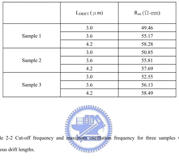
RF LDMOS transistors were fabricated using a 0.5 μm LDMOS process. The schematic cross section of the device is shown in Fig. 2.2. The drain region was extended under the field oxide (FOX) and consisted of a lightly doped N-well drift region and an N- region with higher
eliminate extra surface bond wires to reduce the source inductance and improve the RF performance in a power amplifier configuration [11]. The gate oxide thickness was 135 Å and the mask channel length (LCH) was 0.5μm . The drift length (LDrift=LOV+LFOX) was varied for 3.0μm, 3.6μm, and 4.2μm. For the fishbone structure, three samples with finger width LF=10μm were investigated in this study. Sample 1: with 6 cells, each cell had 2 fingers, and total channel width was W=120μm (see Fig. 2.3(a)). Sample 2: with 12 cells, each cell had 2 fingers, and total channel width was W=240μm. Sample 3: with 4 cells, each cell had 6 fingers, and total channel width was W=240μm (see Fig. 2.3(b)).
2.2.1 DC
Characteristics
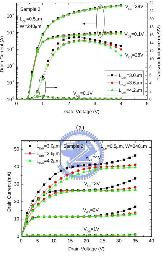
Table 2-1 lists the extracted on-resistance (Ron) for the three samples with various drift length. The Ron was extracted from the linear forward I-V characteristics at gate voltage VGS=2 V and normalized to the total width. For a fixed drift length, the three samples had similar value of Ron. As the drift length increased, the Ron increased due to a larger drain series resistance. Fig. 2.4 shows the I–V characteristics of the LDMOS with different drift length. The device with larger LDrift showed a lower drain current and transconductance. Also, the breakdown voltage was higher with a larger LDrift device. For a larger LDrift, the higher resistance in the drift region leaded to a large voltage drop which increased the carrier velocity and eased to enter the velocity saturation. The velocity saturation in the drift region is called “quasi-saturation” while intrinsic MOS is still in linear operation. This effect is generally observed at high gate voltages. As the device enter the quasi-saturation, the gate control ability decreases which limits the drain current level and delays the transition between linear and saturation regime. At gate voltage VGS=4V in Fig. 2.4(b), larger LDrift made the device enter the saturation slower and limited the drain current level clearly. Also, the transconductance for LDrift=4.2μm in Fig. 2.4(a) started to fall as the gate voltage higher than 3.5V.
2.2.2 High-frequency
Characteristics
To characterize the high-frequency performance, the S-parameters were measured on-wafer from 0.1 to 20 GHz using an HP8510 network analyzer and then de-embedded by subtracting the OPEN dummy. Fig. 2.5 shows the high-frequency characteristics of sample 2 with LDrift=3.0μm. The maximum stable gain/maximum available gain (MSG/MAG) and short-circuit current gain (h21) were calculated from S parameters. The cutoff frequency (fT) and maximum oscillation frequency (fmax) were determined as the frequency where the current gain was 0 dB and the frequency where MAG was 0 dB, respectively. The transistors were measured at drain voltage VDS=28 V with different gate voltages. fT and fmax had maximum values at VGS=2 V, where the transconductance showed a peak. With increasing the gate voltage, both fT and fmax decreased owing to the mobility degradation and quasi-saturation effects.
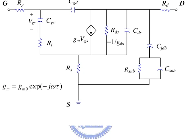
The dependences of the cutoff frequency and maximum oscillation frequency on the drift length for the LDMOS with different geometries are compared in Table 2-2. The transistors were biased at VGS=2 V and VDS=28 V to obtain the maximum value of fT. From Table 2-2, the fT and fmax both decreases with increasing LDrift. By analyzing a MOSFET small-signal equivalent circuit, we can determine the effect of device parameters on high-frequency characteristics more clearly. We adopted a simple model (shown in Fig. 2.6) and extracted the equivalent circuit parameters of the LDMOS by the method described in ref. 12. After de-embedding the extrinsic parasitic resistances and the substrate-related parameters, the intrinsic components can be directly extracted from intrinsic Y-parameters (Yi) by the following equations [13]: ,12 1 Im( ) gd i C Y ω = −
2 ,11 ,11 2 ,11 Im( ) (Re( )) (1 ) (Im( ) ) i gd i gs i gd Y C Y C Y C ω ω ω − = ⋅ + − ,22 ,12 1 Im( ) ds i i C Y Y ω = + ,11 2 2 ,11 ,11 Re( ) (Im( ) ) (Re( )) i i i gd i Y R Y ωC Y = − + ,22 1 Re( ) ds i R Y = 2 2 2 2 2 0 ((Re( ,21)) (Im( ,21) ) ) (1 ) m i i gd gs i g = Y + Y +ωC ⋅ +ω C R ,21 ,21 Im( ) Re( ) 1 sin( gd i gs i i ) m C Y C R Y arc g ω ω τ ω − − − =
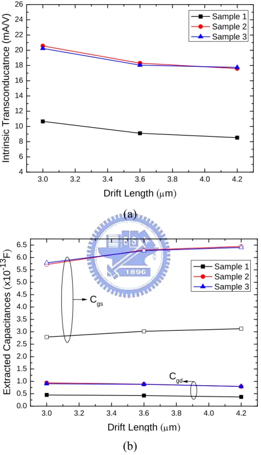
The cutoff frequency can be expressed in a simple way of fT=gm/2π(Cgs+Cgd) which is related to the intrinsic transconductance (gm) and input intrinsic capacitances (Cin=Cgs+Cgd). Fig. 2.7 shows these parameters with respect to the drift length. As the LDrift increased, the decreasing of gm and increasing of Cin resulting in the degradation of fT. In addition, the ratios of gm to Cin were similar for fixed drift lengths which indicate that fT were comparable for these three samples. The approximate maximum oscillation frequency can be expressed as follows: [14] max 4 8 ( ) T DS g T gd g d f f g R + πf C R +αR ∼
From Table 2-2, fmax shows lower value with higher LDrift due to the decreasing of fT and increasing of drain resistance. With fixed LDrift, fmax was similar in sample 1 and 2 but showed higher value in sample 3. Compare sample 1 with sample 2, two times increasing of total finger numbers in sample 2 leaded to two fold increase of Cgd and gds; two fold decrease of Rg and Rd [15]. For having the same finger numbers in each one cell, the devices area also increased two times for sample 2 (i.e. two times in Cjdb). The drain-to-substrate junction capacitance (Cjdb) refers to the deep n-well (DNW) to p-substrate/p-body junction capacitance
(see Fig. 2.2) and this capacitance also has impact on fmax [16]. Therefore, the effects of these parameters were compensated and no variations were observed in fmax. In sample 3, the number of fingers in one cell was 6 rather than 2 in sample 2. This indicates that the device area was lowered than sample 2 and less than two times than sample 1. Consequently, the lower Cjdb can not be canceled by the increase of Rg and Rd; and sample 3 exhibits higher fmax than sample 1 and 2.
2.3 Comparison of Two Layout Design: Fishbone and Ring
The fishbone structure used in this study had 6 cells which each cell had 6 fingers with finger width LF=10μm. For the ring structure, the width of each gate ring was 4×10μm and all the rings were arranged as a 3x3 array in one device. In each ring, the source region was surrounded by the drain region, while the gate was located between the source and the drain (see Fig. 2.1). To compare the performance of the fishbone and ring structures fairly, both structures had the same total channel width (W=360μm).
2.3.1 DC
Characteristics
The I–V characteristics of the LDMOS with different layout structures are shown in Fig. 2.8. In low- and medium-bias regions, the ring structure showed a higher drain current and transconductance than the fishbone structure. This attribute to the lower drain parasitic resistance (Rd). In addition, the breakdown voltage of the ring structure was similar to that of the fishbone structure (VBD≅46-52V for drift length LDrift =3.0-4.2μm). Hence, the ring structure had better DC performance than the fishbone structure. However, when the devices were biased at higher gate and drain voltages, the transconductance and drain current of the ring structure decreased and became smaller than those of the fishbone structure. From the output I–V characteristics of the ring structure, we observed a negative output resistance in the
high-current region. It indicated the self-heating effect in the ring structure was significant due to the compact layout area. With high current density in the transistor, the rise in device temperature due to the dissipated power became significant. The increased device temperature would reduce the carrier mobility and saturation velocity [17]. The device self-heating could be improved by increasing the distance between rings. The drain-source on-resistance is an important parameter for describing the performance of LDMOS transistors. The on-resistance (Ron) was extracted from the linear forward I–V characteristics at gate voltage VGS = 2 V, since it was predominated by the drift region under such a condition. The extracted Ron was plotted against the drift length in Fig. 2.9. As the drift length increased, the on-resistance increased in both structures due to a high drain parasitic resistance. Ron was related to the drain current and was dependent on the drain resistance. Therefore, Ron was lower in the ring structure than that in the fishbone structure and was interpreted as being due to a lower drain resistance.
2.3.2 High-frequency
Characteristics
The dependences of the cutoff frequency and maximum oscillation frequency on the drift length for the LDMOS with different layout structures are compared in Fig. 2.10. The transistors were biased at VGS=2 V and VDS=28 V to obtain the maximum value of fT. It was observed that fT and fmax both decreased with increasing LDrift because the gm decreased and both Cin and drain resistance increased with increasing LDrift. In Fig. 2.10, we also found that
fT and fmax for the ring structure had higher values than those for the fishbone structure. This might be attributed to the reduction of drain parasitic resistance. In addition, the difference in
fmax between the fishbone and ring structures was larger than the difference in fT.
By analyzing a MOSFET small-signal equivalent circuit, we can determine the effect of device parameters on high-frequency characteristics more clearly. Using extracted parameters from the existing device and altering one parameter at the time, the effect of model
parameters on the cutoff frequency and maximum oscillation frequency can be visualized. The influences of model parameters on fT and fmax are shown in Fig. 2.11. The x-axis showed the parameter value departure from the initial value in percent. The y-axis showed the change in frequency in percent. Parameters not shown in the figure had approximately the same value for the ring and fishbone structures or had a minor influence on fT and fmax. Table 2-3 lists the parameters that have more influence on fT and fmax for the fishbone structures with different drift length. When LDrift shorten to 3.0 μ m, transconductance (gm) and gate-source capacitance (Cgs) were the two major parameters that improve the fT and fmax. To investigate the superior high-frequency performance on ring structure, parameters that affect the fT and
fmax were analysis for fishbone and ring. The parameters that affect fT more significantly (see Fig. 2.11(a)) are listed in Table 2-4. In conventional MOSFET, the intrinsic parameters, gm, Cgs, and gate-drain capacitance (Cgd), were usually considered to explain the change in cutoff frequency due to the simple express fT=gm/2π(Cgs+Cgd). However, the existence of the drift region in LDMOS makes the extrinsic parameter, drain resistance (Rd), become more important and can not be ignored. Rd represents the drain contact resistance and part of the drift region. As Rd decreased from 18.06 Ω to 7.789 Ω, fT could be improved by as much as 3.56% for the ring structure. In addition, the lower Cgd and higher Cgs in the ring structure caused about 1.57% and -2.8% changes in fT due to different layout design. As for gm and drain-to-substrate junction capacitance (Cjdb), the impact on fT was too small to be considered. By analyzing fmax, we found that the intrinsic parameters like gm, Cgs, and Cgd, showed a minor influence when we changed the device structure. Hence, we only considered the influence of extrinsic parameters. The extrinsic parameters that affected fmax more significantly (see Fig. 2.11(b)) are listed in Table 2-5. As Rd decreased from 18.06 Ω to 7.789 Ω, fmax could be improved by as much as 21.5% for the ring structure. In addition, the lower Cjdb in the ring structure also increases fmax by about 14.27%, due to the smaller device area.
decreased fmax by about 10.52%. Using the ring structure, we estimated that fT improved by about 2.72% (fT was 3.77 GHz for the ring structure and 3.67 GHz for the fishbone structure) and fmax improved by about 24.5% (fmax was 10.18 GHz for the ring structure and 8.183 GHz for the fishbone structure). Therefore, Rd could be the key factor for improving fT and fmax by using the ring structure.
Figure 2.12 shows the extracted drain parasitic resistance versus the drift length for LDMOS transistors with different layout structures. As LDrift increased, the drain parasitic resistance increased. Note that for higher breakdown voltages, LDrift needed to be longer, resulting in poor on-resistance, fT, and fmax. Nevertheless, Ron and fmax for the ring structure appeared superior to those for the fishbone structure. The improvements of DC and RF characteristics were attributed to the minor drain resistance (see Fig. 2.12). The drain region of the ring structure had extra areas (the shaded regions) compared with the fishbone structure, and the extra areas would have lowered the drain parasitic resistance, as shown in the inset of Fig. 2.12.
2.3.3
RF Power and Linearity
As well as the high-frequency characteristics, the microwave power characteristics were also investigated using the load-pull measurement. In our study, the input was terminated to 50 ohms and the load impedances were tuning for maximum output power. For having the value of fmax in the range from 8 GHz to 11 GHz, the devices were measured at 900 MHz with gate bias VGS=2 V and drain bias VDS=28 V. Figure 2.13 shows the output power, power gain and power added efficiency (PAE) with different drift lengths. In Fig. 2.13, the power characteristics were similar among these two transistors at low input power and show discrepancy when input power was larger than 1-dB compression point (P1db). The main reason for gain compression was attributed to the clipping effect. The border of output I-V curve will cause output waveform to be clipped for MESFET, PHEMT and HBT [18-20]. The
clipping effect can also been found in LDMOS. Figure 2.14 shows the drain current versus gate voltage with input and output waveform for different drift lengths. Part of the AC-signals on the drain current would be cut off as the input power becomes larger enough. At this condition, the average drain current increased with the increasing input power (see Fig. 2.15) and the power gain has been compressed. This is because the dynamic load line exceeds the border of DC I-V. As the drift length increased, larger on-resistance decreased the drain current which makes the negative duty cycle of output waveform enter the cutoff region earlier. This indicates that the average drain current started to increase earlier (see Fig. 2.15) and the gain compression occurs prior. Consequently, the transistor with longer drift length showed lower value of output power, power gain and PAE when input power was larger than P1db. Figure 2.16 shows the RF power characteristics for different layout structures. The ring structure exhibits a better performance than the fishbone.
Since the dc behaviors were changed, the linearity would also be affected with various drift lengths. The input and output third-order intercept points (IIP3 and OIP3) for fishbone with various drift lengths are listed in Table 2-6. Also, the ring and fishbone for fixed LDrift =3.6μm were compared. For the fishbone structures, the transistor with longer drift length showed poor linearity. With fixed LDrift, IIP3 and OIP3 was similar in the fishbone and ring structure (as shown in Fig. 2.17).
2.4 Summary
Fishbone with various layout designs for RF applications were investigated. The structure with smaller LDrift has better on-resistance, fT, fmax, and linearity, but smaller breakdown voltage. It shows a trade-off between the on-resistance and the breakdown voltage in the conventional LDMOS. Fishbone and ring structures for RF applications were also compared. The ring structure had a better performance than the fishbone structure, without
altering the process flow. The higher drain current and transconductance in the LDMOS with the ring structure were due to lower drain parasitic resistance. In addition, the fT and fmax were also enhanced for the ring structure due to the lower drain parasitic resistance. Our results suggested that, using a ring structure, a higher breakdown voltage can be achieved using a longer LDrift without degrading DC and RF characteristics.
References
[1] S. P. Voinigescu, S. W. Tarasewicz, T. MacElwee, and J. Ilowski, “An assessment of the state-of-the-art 0.5 μm bulk CMOS technology for RF applications,” IEDM Tech. Dig., Dec. 1995, pp. 721–724.
[2] C. S. Kim, H. K. Yu, H. Cho, S. Lee, and K. S. Nam, “CMOS layout and bias optimization for RF IC design applications,” IEEE MTT-S Digest, pp. 945-948. 1997.
[3] H. Lee, J. H. Lee, Y. J. Park, and H. S. Min, “Characterization issues of gate geometry in multifinger structure for RF-SOI MOSFETs,” IEEE Electron Device Lett., vol. 23, No. 5, pp. 288-290, May 2002.
[4] M. M. De Souza, G. Cao, E. M. Sankara Narayanan, F. Youming, S. K. Manhas, J. Luo, and N. Moguilnaia, “Progress in silicon RF Power MOS technologies - current and future trends,” in Proc. International Caracas Conf. Devices, Circuits and Systems (ICCDCS), 2002, pp. D047 (1 – 7).
[5] R. Yang, J. F. Li, H. Qian, G. Q. Lo, N. Balasubramanian, and D. L. Kwong, “A Short-Channel SOI RF Power LDMOS Technology With TiSi2 Salicide on Dual Sidewalls With Cutoff Frequency fT ~19.3GHz,” IEEE Electron Device Lett., vol. 27, No. 11, pp. 917-919, Nov. 2006.
[6] P. L. Hower and M. J. Geisler, “Comparison of various source-gate geometries for power MOSFET's,” IEEE Trans. Electron Devices, vol. 28, no. 9, pp. 1098-1101, 1981.
[7] P. L. Hower, T. M. S. Heng, and C. Huang, “Optimum design of power MOSFETs,”
IEDM Tech. Dig., Dec. 1983, pp. 87–90.
[8] C. Hu, M. H. Chi, and V. M. Patel, “Optimum design of power MOSFETs,” IEEE Trans.
Electron Devices, vol. 31, no. 12, pp. 1693-1700, 1984.
[9] K. Board, D. J. Byrne, and M. S. Towers, “The optimization of on-resistance in vertical DMOS power devices with linear and hexagonal surface geometries,” IEEE Trans.
[10] J. Fernandez, S. Hidalgo, J. Paredes, F. Berta, J. Rebollo, J. Millan, and F. S. Mestres, “An ON-resistance closed form for VDMOS devices,” IEEE Electron Device Lett., vol. 10, No. 5, pp. 212-215, May 1989.
[11] F. M. Rotella, G. Ma, Z. Yu, and R. W. Dutton, “Modeling, analysis, and design of RF LDMOS devices using harmonic-balance device simulation,” IEEE Trans. Microwave
Theory Tech., vol. 48, No. 6, pp. 991-999, Jun 2000.
[12] S. C. Wang, G. W. Huang, K. M. Chen, A. S. Peng, H. C. Tseng, and T. L. Hsu, “A Practical Method to Extract Extrinsic Parameters for the Silicon MOSFET Small-Signal Model,” in Proc. NSTI Nanotechnology Conference & Trade Show (Nanotech 2004), 2004 p. 151-154.
[13] J. Jang, O. Tornblad, T. Arnborg, Q. Chen, K. Banerjee, Z. Yu, and R. W. Dutton, “RF LDMOS characterization and its compact modeling,” IEEE MTT-S Digest, pp. 967-970. 2001.
[14] T. C. Lim and G. A. Armstronga, “The impact of the intrinsic and extrinsic resistances of double gate SOI on RF performance,” Solid-State Electron., vol. 50, pp. 774-783, 2006. [15] C. S. Kim, H. K. Yu, H. Cho, S. Lee, and K. S. Nam, “CMOS layout and bias
optimization for RF IC design applications,” IEEE MTT-S Digest, pp. 945-948. 1997. [16] W. Wu, S. Lan, P. K. Ko, and M. Chan, “Characterization and modeling of waffle
MOSFETs for high frequency applications,” in Proc. IEEE Solid-State and Integrated
Circuits Tech. Conf., 2004, pp. 163-166.
[17] M. A. Belaid, K. Ketata, H. Maanane, M. Gares, K. Mourgues, and J. Marcon, “Analysis and simulation of self-heating effects on RF LDMOS devices,” in Proc. IEEE SISPAD, 2005, pp. 231-234.
[18] C. C. Meng, A. S. Peng, S. Y. Wen and G. W. Huang, “Direct Observation of Gain Compression Mechanisms in PHEMT by RF Gate and Drain Currents,” in Proc.
Sep. 2002, pp. 241- 244.
[19] C. C. Meng, C. H. Chang, J. E Kuan and G. W. Huang, “Direct Observation of Loadlines in MESFET by Using Average RF Gate and Drain Currents,” IEEE MTT-S Digest, pp. 2161-2164. 2002.
[20] A. S. Peng, K. M. Chen, G. W. Huang, M. H. Cho, S. C. Wang, Y. M. Deng, H. C. Tseng, and T. L. Hsu, “Temperature Effect on Power Characteristics of SiGe HBTs,” IEEE
Table 2-1 The extracted on-resistances for three samples with various drift lengths. LDRIFT (μm) Ron (Ω-mm) 3.0 49.46 3.6 55.17 Sample 1 4.2 58.28 3.0 50.85 3.6 55.81 Sample 2 4.2 57.69 3.0 52.55 3.6 56.13 Sample 3 4.2 58.49
Table 2-2 Cut-off frequency and maximum oscillation frequency for three samples with various drift lengths.
LDRIFT (μm) fT (GHz) fmax (GHz) 3.0 4.50 7.91 3.6 3.75 6.91 Sample 1 4.2 3.56 6.68 3.0 4.20 7.76 3.6 3.62 6.94 Sample 2 4.2 3.48 6.34 3.0 4.32 8.64 3.6 3.68 7.87 Sample 3 4.2 3.54 6.95
Table 2-3 Extracted gm, Rd, Cgd, and Cgs for fishbone structure with various drift lengths. The
fT and fmax differences between the LDrift=3.6μm and 3.0μm due to the change of model parameters are also listed.
gm (A/V) Rd (Ω) Cgd (F) Cgs (F) Fishbone LDrift=3.6μm 29.69m 16.05 133.5f 877.2f Fishbone LDrift=3.0μm 27.08m 18.06 130.0f 951.0f fT Difference 8.87% 0.68% -0.48% 6.77% fmax Difference 6.88% 2.78% -0.86% 5.4%
Table 2-4 Extracted gm, Rd, Cgd, Cgs, and Cjdb for different layout structures. The fT differences between the fishbone and ring structures due to the change of model parameters are also listed. gm (A/V) Rd (Ω) Cgd (F) Cgs (F) Cjdb (F) Fishbone LDrift=3.6μm 27.08m 18.06 130.0f 951.0f 244f Ring LDrift=3.6μm 27.11m 7.789 119.0f 985.0f 149f fT Difference 0.11% 3.56% 1.57% -2.8% 0.1%
Table 2-5 Extracted Rd, Cjdb, and Rg for different layout structures. The fmax differences between the fishbone and ring structures due to the change of model parameters are also listed. Rd (Ω) Cjdb (F) Rg (Ω) Fishbone LDrift=3.6μm 18.06 244f 1.997 Ring LDrift=3.6μm 7.789 149f 4.489 fmax Difference 21.5% 14.28% -10.52%
Table 2-6 IIP3 and OIP3 for different layout structures with various drift length
IIP3 (dBm) OIP3 (dBm) Fishbone LDrift=3.0μm 29.18 41.60 Fishbone LDrift=3.6μm 21.84 34.31 Ring LDrift=3.6μm 21.51 34.29
(a) (b)
(a)
(b)
Fig. 2.3 Fishbone layout structures: (a) Sample 1 and (b) Sample 3.
Total channel width=120μm
Sample 1
Gate
Drain
Source
Finger
Width
Sample 3
Drain
Total channel width=240μm
Source
Finger
Width
0 1 2 3 4 5 10-7 10-6 10-5 10-4 10-3 10-2 0 2 4 6 8 10 12 14 16 18 20 22 24 LCH=0.5μm W=240μm VDS=28V VDS=28V VDS=0.1V Tra n sco nd uc ta nc e (m A/V) D ra in C u rre nt (A) Gate Voltage (V) LDrift=3.0μm LDrift=3.6μm LDrift=4.2μm VDS=0.1V Sample 2
(a)
0 5 10 15 20 25 30 35 40 0 10 20 30 40 50 Drain Current (mA) Drain Voltage (V) L Drift=3.0μm L Drift=3.6μm L Drift=4.2μm L CH=0.5μm, W=240μm VGS=1V VGS=2V VGS=3V V GS=4V Sample 2(b)
Fig. 2.4 (a) Subthreshold and (b) output characteristics of LDMOS transistors with different drift lengths.
(a)
(b)
Fig. 2.5 Dependence of (a) |h21| and (b) MSG/MAG on frequency obtained from S-parameter measurements. 108 109 1010 1011 -20 -10 0 10 20 30 40 Sample 2 VDS=28V LDrift= 3.0 μm LCH= 0.5 μm, W = 240 μm |h 21 | (dB) Frequency (Hz) V GS=1V VGS=2V V GS=3V V GS=4V fT 108 109 1010 1011 -20 -10 0 10 20 30 Sample 2 LDrift= 3.0 μm LCH= 0.5 μm, W = 240 μm MS G/MAG ( d B) Frequency (Hz) V GS=1V VGS=2V V GS=3V V GS=4V fmax VDS=28V
Fig. 2.6 A simple equivalent circuit model of the LDMOS.
R
gR
dR
sC
gsR
iR
subR
ds=1/g
dsC
subC
gdC
dsC
jdbg
mV
gsG
D
S
0exp(
)
m mg
=
g
−
j
ωτ
V
gs + _(a)
(b)
Fig. 2.7 (a) Intrinsic transconductance and (b) Cgs and Cgd versus drift length with different samples. 3.0 3.2 3.4 3.6 3.8 4.0 4.2 4 6 8 10 12 14 16 18 20 22 24 26 In tr insic T ransconducat nce (mA/ V) Drift Length
(
μm)
Sample 1 Sample 2 Sample 3 3.0 3.2 3.4 3.6 3.8 4.0 4.2 0.0 0.5 1.0 1.5 2.0 2.5 3.0 3.5 4.0 4.5 5.0 5.5 6.0 6.5 Cgd Ext racted Capacit ances(
x10 -1 3 F)
Drift Length(
μm)
Sample 1 Sample 2 Sample 3 Cgs0 1 2 3 4 5 10-7 10-6 10-5 10-4 10-3 10-2 10-1 0 5 10 15 20 25 30 35 VDS=0.1V VDS=28V T ranscond uct a nce (m A/ V) LCH= 0.5 μm W = 360 μm LDrift=3.6μm VDS=28V VDS=0.1V Drain Current (A) Gate Voltage (V) Fishbone Ring
(a)
0 10 20 30 40 0 20 40 60 80 VGS=1V VGS=2V VGS=3V VGS=4V D rai n C u rrent (m A) Drain Voltage (V) Fishbone Ring LCH=0.5μm, W=360μm, LDrift=3.6μm(b)
Fig. 2.8 (a) Subthreshold and (b) output characteristics of LDMOS transistors with different layout structures.
Drift Length (μm) 2 3 4 5 On-resistance ( Ω -mm) 10 15 20 25 30 35 40 Fishbone Ring
2.8 3.0 3.2 3.4 3.6 3.8 0 2 4 6 8 10 12 14 fmax LCH=0.5μm W=360μm F requenc y (GHz) Drift Length (μm) Fishbone Ring VDS=28V, VGS=2V fT
-50 -40 -30 -20 -10 0 10 20 30 40 50 -20 -15 -10 -5 0 5 10 15 20 gm Changes i n f T (% )
Changes in parameter value (%)
Cjdb
Cgs
Rd
Cgd
-50 -40 -30 -20 -10 0 10 20 30 40 50 -20 -15 -10 -5 0 5 10 15 20 Rd Cgd Cjdb Cgs Rg Csub Changes i n f MA X (%)
Changes in parameter value (%)
Rsub
2.4 2.8 3.2 3.6 4.0 4.4 4.8 4 6 8 10 12 14 16 18 20 22 24 26 Dr ai n Res is ta nc e ( Ω ) Drift Length (μm) Fishbone Ring LCH= 0.5 μm W = 360 μm Finger Width S Drain Finger Width S Drain Finger Width S Drain
Fig. 2.12 Rd versus LDrift for LDMOS with different layout structures. The inset shows that the drain region of the ring structure had extra areas (the shaded regions) compared with the fishbone structure.
-20 -10 0 10 20 -10 -5 0 5 10 15 20 25 30 0 4 8 12 16 20 24 28 32 36 Fishbone VGS=2V, VDS=28V freq= 900MHz Power Ad ded E ff iciency (%) Po w e r Ga in ( d B) , Ou tp u t P o w e r ( d B m ) Input Power (dBm) LDrift=3.0μm LDrift=3.6μm Pout Gain PAE
Fig. 2.14 Drain current versus gate voltage with different drift lengths. The input signal was bias at VGS=2V and the negative duty cycle of output signal was clipped by the cutoff region.
Cutoff Condition 0 1 2 3 4 0 10 20 30 40 50 60 70
I
DS (A) VGS (V) LDrift=3.0μm LDrift=3.6μm VDS=28VP
inincrease
Output drain
current waveform
-20 -10 0 10 20 18 20 22 24 26 28 30 32 34 36 38 LDrift=3.0μm LDrift=3.6μm
Average Drain Current
(m A) Input Power (dBm) Fishbone VGS=2V, VDS=28V freq= 900MHz
-20 -10 0 10 20 -10 -5 0 5 10 15 20 25 30 0 4 8 12 16 20 24 28 32 36 Po w e r Gai n (dB ), Ou tp ut Po w e r (d Bm ) Input Power (dBm) Fishbone Ring Pout Gain PAE VGS=2V, VDS=28V freq= 900MHz LDrift=3.6μm Po we r Ad de d Efficie n c y (% )
Fig. 2.16 Output power, power gain and PAE versus input power with different layout structures.
-10 -5 0 5 10 15 20 25 -70 -60 -50 -40 -30 -20 -10 0 10 20 30 40 34.31 dBm freq= 900MHz 21.5 dBm OIP3 VGS=2V VDS=28V Output
Power & IM3
(dBm) Input Power (dBm) Fishbone Ring Output Power IM3 IIP3 21.8 dBm 34.28 dBm
Fig. 2.17 Output power and third-order intermodulation power versus input power with different layout structures.
Chapter 3
Thermal Effects on DC and RF Performances of RF LDMOS
3.1 Introduction
For high-power applications, temperature is an important issue. The cutoff frequency (fT) and maximum oscillation frequency (fmax) are critical figures of merit for evaluating the performance of RF transistors. For conventional MOS transistors in RF applications, the temperature effect was investigated by studying the temperature dependence of fT, which is proportional to the transconductance [1]. With an increase in temperature, the fT and fmax have been shown to decrease. According to its structure, the parasitic drain resistance of the LDMOS becomes more important than that of the conventional MOSFET for the present drift region. However, in most of the studies, the effect of the parasitic resistance was not considered when analyzing the temperature effect on the device characteristics [1-3]. By de-embedding the effect of the parasitic source and drain resistors from the measured S-parameters, the temperature dependence of the intrinsic fT can be analyzed. Several researchers have investigated the effects of temperature on the reliability and dc performances of LDMOS transistors [4-6]. However, the temperature effects on the high-frequency characteristics of LDMOS have seldom been addressed.
In this chapter, the DC and high-frequency characteristics of LDMOS transistors with different layout structures were studied at various temperatures. To study the self-heating effect, the pulsed current-voltage (I-V) and RF characteristics of LDMOS transistors are also discussed. The differences between the cw- and pulsed-mode measurements on drain current, cutoff frequency and maximum oscillation frequency are compared.