國立交通大學
材料科學與工程學研究所
碩士論文
磷化銦鎵高電子遷移率電晶體暨砷化銦鎵金氧半
高電子遷移率電晶體於高頻與數位應用之探討
Study of InGaP HEMTs and In
xGa
1-xAs
MOS-HEMTs for RF and Digital Applications
研究生 鍾榮濤
指導教授 張 翼 博士
磷化銦鎵高電子遷移率電晶體暨砷化銦鎵金氧半高電子遷移率
電晶體在高頻與數位應用之探討
Study of InGaP HEMTs and In
xGa
1-xAs
MOS-HEMTs for RF and digital applications
研 究 生:鍾榮濤 Student: Jung-Tao Chung 指導教授:張 翼 博士 Advisor: Dr. Edward Yi Chang
國立交通大學
材料科學與工程研究所
碩士論文
A Thesis Submitted to Department of Materials Science and Engineering College of Engineering
National Chiao Tung University In Partial Fulfill of the Requirements
For the Degree of Master of Science
In Material Science and Engineering August 2008
Hsinchu, Taiwan, Republic of China
磷化銦鎵高電子遷移率電晶體暨砷化銦鎵
金氧半高電子遷移率電晶體於高頻與數位
應用之探討
研究生: 鍾榮濤 指導教授: 張 翼 博士 國立交通大學材料科學與工程學系摘要
不同載子參雜方式的磷化銦鎵高電子遷移率電晶體的高頻與數 位特性在此被研究。在高頻無線通訊應用上,為了要提升線性度,載 子被均勻參雜於蕭基層與參雜載子於通道層。以均勻參雜載子的方式 製成之元件,三階交叉點可達 22.19 dBm;通道參雜載子的方式製成 之元件線性工作範圍達 14.23 dB,並且三階交叉點電源損耗比值接近 4.97。在數位邏輯應用上,均勻參雜載子的方式製成之元件可提升次 臨線傳導斜率,以及開關電流比值;通道參雜載子的方式製成之元件 的短通道效應也有所降低。 在數位應用時,高銦含量的砷化銦鎵通道材料是必須的,使元件 能具有好的數位特性表現以及較高速的轉導特性。以原子層沉積氧化 鋁做為閘極絕緣層也能降低漏電流並提高崩潰電壓。砷化銦鎵金氧半 假晶式高電子遷移率電晶體和砷化銦金氧半高電子遷移率電晶體被 製作出來並展現出良好的絕緣性。此外,將空橋結構應用於砷化銦金氧半高電子遷移率電晶體做出不同閘極寬度的元件,可做為數位應用 上不同扇出層級之元件。
Study of InGaP HEMTs and In
xGa
1-xAs
MOS-HEMTs for RF and Digital
Applications
Student: Jung-Tao Chung Advisor: Dr. Edward Y. Chang Department of Materials Science and Engineering
National Chiao Tung University
Abstract
The RF and digital performance of InGaP/In0.22Ga0.78As
pseudomorphic high electron mobility transistors (PHEMTs) with different doping profiles are investigated. In order to improve the device linearity for RF applications, the uniformly-doped and channel-doped structures are designed and the devices are compared. The uniformly- doped device shows higher IP3 of 22.19 dBm, and the channel-doped device shows higherΔ (IP3-P1dB) of 14.23 dB and higher IP3 to DC
power consumption ratio (IP3/PDC) of 4.97 compared to other devices.
Figures of merits of these devices for digital applications are also evaluated. SS and ION/IOFF ratio parameters can be improved by
uniformly-doping in the Schottky layer and DIBL parameter can be reinforced by extra doping in the channel layer.
For digital applications, the InGaAs channel with high indium concentration is required for better performance and higher transconductance. In addition, atomic layer deposition (ALD) Al2O3 is
metal-oxide-semiconductor metamorphic HEMTs (MOS-MHEMTs) and InAlAs/InAs MOS-HEMTs were fabricated and the insulating properties were improved. Moreover, the InAlAs/InAs MOS-HEMTs employing air-bridge structure with different gate widths exhibit similar threshold voltage, leading to the possibility for digital utilization of different fan-out level.
誌謝
兩年時光悄然而逝,在不斷的犯錯中成長,在試片堆中磨練不屈 的意志,最後留下了數不盡的感激。首先要感謝張翼教授,在外忙碌 奔波募集儀器設備和實驗資源的同時,也肯抽出空閒對我諄諄善誘。 謝謝一直悉心帶著我做實驗的林岳欽學長,除了日常學業上的討論與 教導之外,也教會了我如何解決問題以及做人處事的道理。謝謝吳雲 驥學長、張家達學長、許立翰學長在實驗上的協助,讓我學到了面對 實驗的態度,一直都是我心目中的典範。此外,真心感謝黃延儀學長、 郭建億學長、張家源學長、黃瑞乾學長、陳克弦學長、唐士軒學長對 我的種種協助與鼓勵,由衷感激。當然也不會忘了一起奮鬥的蕭世匡 同學、蕭佑霖同學、謝勝禮同學、胡志偉同學、黃偉進同學、曾郁玲 同學、王景德同學、黃曼琪同學、施琳琪同學,和你們在一起的同聲 歡笑是實驗室最美麗的點綴。謝謝吳建瑩學弟、陳鈺霖學弟、宋先敏 學弟、蔡思屏學妹、蘇詠萱學妹和陳奕仲學弟,謝謝你們在畢業典禮 時所獻上誠摯的祝福,是我永難忘懷的生日禮物。另外也要謝謝親愛 的助理小姐們,帥氣的李芳銘先生、詹前章先生和黃碧玉小姐一直以 來在各方面的幫助,讓許多行政事務得以運作。 最後感謝所有被我做壞的wafer,在背後默默聲援我的父母家人 和傻氣的女朋友,你們的支持給了我堅持下去的勇氣。謝謝你們!Content
Abstract (Chinese) ... Ⅰ
Abstract (English) ··· Ⅲ
Acknowledgments ...Ⅴ
Content ... VI
Table Captions ... X
Figure Captions ... XI
Chapter 1 Introduction
1.1 General Background ... 1
1.2 Thesis Content ... 3
Chapter 2 Literature Review
2.1 HEMTs for digital applications ... 5
2.2 Logic parameters for low-power application ... 6
2.3 MOS-HEMTs fabrication ... 7
2.4 Surface treatment ... 7
Chapter3 Fundamentals of Electrical Characteristics
3.1 Device model ... 9
3.2 Noise figure (NF) ... 11
3.4 Breakdown voltage (BV
gd) ... 14
3.4.1 Physics for device breakdown ... 14
3.4.2 Analytic model for design ... 15
3.4.3 Improvement of the breakdown voltage ... 17
3.5 Extrinsic transconductance (g
m) ... 19
3.6 Unit current gain cut-off frequency (f
T) and maximum
frequency of oscillation (f
max) ... 19
Chapter4 RF and Digital Performance of HEMTs
with Different Doping Profiles
4.1 Introduction ... 27
4.2 Device Fabrication ... 28
4.2.1 Wafer cleaning ... 29
4.2.2 Mesa isolation ... 29
4.2.3 Ohmic formation ... 29
4.2.4 Recess and gate formation ... 30
4.2.5 Device passivation ... 31
4.2.6 Air-bridge plating ... 32
4.3 Results and discussion ... 32
4.3.1 Devices for RF applications ... 32
4.3.2 Devices for Logic applications ... 34
Chapter5 Introducing Al
2O
3as Gate Insulator for
InAlAs/In
0.7Ga
0.3As MOS-MHEMTs Fabrication
5.1 Introduction ... 47
5.2 Device Fabrication ... 48
5.2.1 Wafer cleaning ... 49 5.2.2 Mesa isolation ... 50 5.2.3 1st recess ... 50 5.2.4 Surface treatment ... 505.2.5 Atomic layer deposition (ALD) Al2O3 ... 51
5.2.6 Ohmic formation ... 51
5.2.7 Gate formation ... 52
5.3 Results and discussion ... 52
5.4 Conclusions ... 54
Chapter6 Employing Air-bridge Structure on InAlAs/
InAs MOS-HEMTs for Digital Applications
6.1 Introduction ... 59
6.2 Device Fabrication ... 60
6.2.1 Wafer cleaning ... 61 6.2.2 Mesa isolation ... 61 6.2.3 1st recess ... 61 6.2.4 Surface treatment ... 626.2.6 Ohmic formation ... 62
6.2.7 Gate formation ... 63
6.2.8 Device passivation ... 63
6.2.9 Air-bridge plating ... 64
6.3 Results and discussion ... 65
6.4 Conclusions ... 66
Chapter7 Conclusions ... 71
Table Captions
Table 4-1 Comparison of the DC characteristics of the three
different types of devices
... 37Table 4-2
Comparison of the IP3 of the three different types of devices ... 37Table 4-3 Logic parameters of the 0.3μm InGaP/In
0.22Ga
0.78As
PHEMTs with different doping profiles
... 38Table 5-1 Comparison of relevant properties for high-K
candidates ...
55Table 5-2 Logic parameters of the 0.8μm InAlAs/In
0.7Ga
0.3As
MOS- MHEMT and conventional HEMT
... 55Table 6-1
Logic parameters of the 0.8μm InAlAs/InAs MOS-HEMT with various gate widths……….67Figure Captions
Fig. 1-1 Cutoff frequency versus power dissipation curves of HEMTs and
Si-MOS ... 4
Fig. 1-2 Energy band gap versus lattice constant diagram of III-V materials………..4
Fig. 2-1 The definition of threshold voltage (VT) and ION/IOFF ratio. ... 8
Fig. 2-2 The definition of subthreshold slope (SS) and drain induced barrier lower (DIBL). ... 8
Fig. 3-1 PHEMT small signal device model. ... 23
Fig. 3-2 PHEMT equivalent circuit with noise source ... 23
Fig. 3-3 Output power diagram of fundamental andthird-order product signals.. ... 24
Fig. 3-4 Fundamental diagram of the microwave front-end device... 24
Fig. 3-5 A schematic cross-section of the InAlAs/InGaAs PHEMT. ... 25
Fig. 3-6 Dependence of the breakdown voltage (BVgd) on the gate recess width ... 25
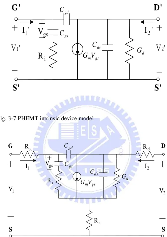
Fig. 3-7 PHEMT intrinsic device model ... 26
Fig. 3-8 PHEMT small signal equivalent circuit ...26
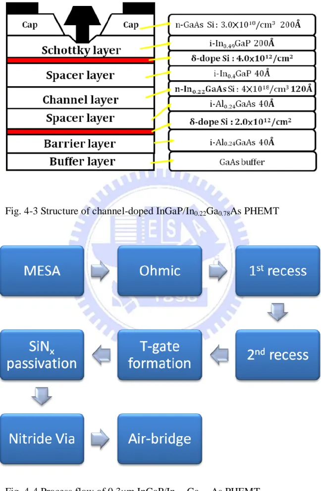
Fig. 4-1Structure of δ-doped InGaP/In0.22Ga0.78As PHEMT ...39
Fig. 4-2 Structure of uniformly-doped InGaP/In0.22Ga0.78As PHEMT. ... 39
Fig. 4-3 Structure of channel-doped InGaP/In0.22Ga0.78As PHEMT . ... 40
Fig. 4-4 Process flow of 0.3μm InGaP/In0.22Ga0.78As PHEMT ... 40
Fig. 4-5 IDS vs. VDS curves for the three different types of 0.25 x 160 m 2 devices: (a)δ -doped device, (b) Channel doped PHEMT, (c) Uniformly-doped PHEMT ... 41
Fig. 4-6 (a) Extrinsic transconductance (Gm) vs. VGS curves, (b) IDS
vs.VGS curves for the three different types of devices studied, the
device size is 0.25 × 160 m2 and the VDS bias is 1.5V ... 43
Fig. 4-9 Subthreshold characteristics of the 0.3×200μm2 InGaP/
In0.22Ga0.78As PHEMTvdevices……… 45
Fig. 4-7 IP3 vs. IDS curves of the three 0.25x160μ m2 InGaP/InGaAs
PHEMTs in this study, the test frequency is 5.8GHz and
VDS=1.5V.………. ... 44
Fig. 4-8 Extrinsic transconductance (Gm) versus gate-to-source voltage
(VGS) curves of the 0.3×200μm2 InGaP/In0.22Ga0.78As PHEMT
devices………. ... 44 Fig.4-9 Subthreshold characteristics of the 0.3×200μm2 InGaP/
In0.22Ga0.78As PHEMTvdevices………... 45
Fig. 4-10 Gate leakage current of the 0.3×200μm2 InGaP/In0.22Ga0.78As
PHEMT devices. ... 45 Fig. 4-11 Gate-to-drain breakdown voltage (BVDG) of the 0.3×200μm2
InGaP/In0.22Ga0.78As PHEMT devices ... 46
Fig. 5-1 Structure of 0.8μm InAlAs/In0.7Ga0.3As MOS- MHEMT ... 56
Fig. 5-2 Process flow of 0.8μm InAlAs/In0.7Ga0.3As MOS- MHEMT. .. 56
Fig. 5-3 Drain current (ID) versus the drain voltage (VD) curves of the
0.8μm InAlAs/In0.7Ga0.3As MOS- MHEMT and conventional
HEMT ... 57 Fig. 5-4 Extrinsic transconductance (Gm) versus gate-to-source voltage
(VGS) curves of the 0.8μm InAlAs/In0.7Ga0.3As MOS- MHEMT
Fig. 5-5 Gate-to-drain breakdown voltage (BVDG) of the 0.8μm InAlAs/
In0.7Ga0.3As MOS- MHEMT and conventional
HEMT……….……….… ... 58 Fig. 5-6 Gate leakage current density performance of the 0.8μm
InAlAs/In0.7Ga0.3As MOS- MHEMT and conventional
HEMT… ... 58 Fig. 6-1 Structure of 0.8μm InAlAs/InAs MOS- HEMT ... 68 Fig. 6-2 Process flow of 0.8μm InAlAs/InAs MOS-HEMT ... 68 Fig. 6-3 Extrinsic transconductance (Gm) versus gate-to-source voltage
(VGS) curves of the 0.8μm InAlAs/InAs MOS-HEMT…... ... 69
Fig. 6-4 Drain current (ID) versus gate-to-source voltage (VGS) curves of
the 0.8μm InAlAs/InAs MOS-HEMT.. ... 69 Fig. 6-5 Gate-to-drain breakdown voltage (BVDG) of the 0.8μm
InAlAs/InAs MOS- MHEMT ... 70 Fig. 6-6 Gate leakage current density performance of the 0.8μm
1
Chapter 1
Introduction
1.1 General Background
The RF and digital performance of high electron mobility transistors (HEMTs) have been widely investigated. For high frequency wireless communication, as the density in information traffic increasing, the requirements of device linearity become more demanding. In addition, the device linearity could be improved by varying the doping profiles. The device linearity of InGaP/InGaAs HEMTs with different doping profiles will be discussed in this dissertation.
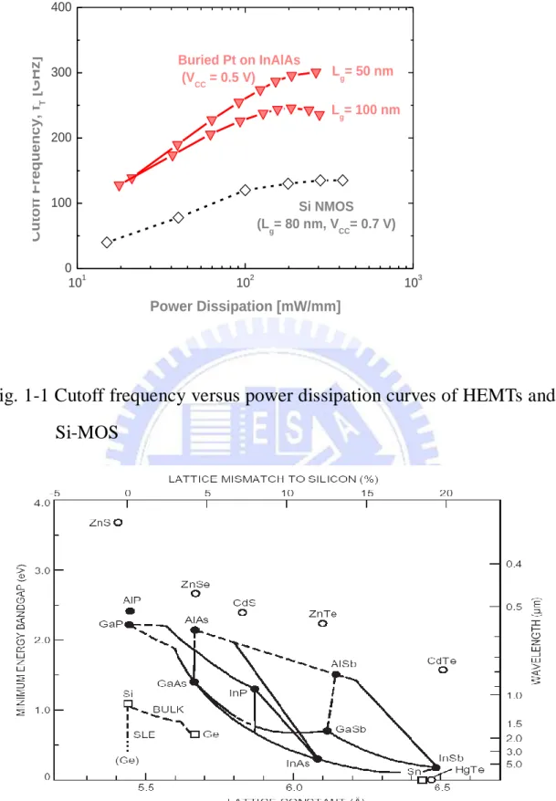
For digital applications, recent years have seen that high electron mobility transistors (HEMTs) have attracted more attention because it is a potential candidate for future low-power logic applications[1]. Current Si technology roadmap is expected to come to the end when the physical gate length is shrunk to 10 nm which is believed to be the scaling limit for CMOS. For the next generation device technology, endowed with high electron mobility, III-V material HEMTs exhibit superior device performance such as higher transconductance, higher current density, lower power consumption and higher operating frequency in comparison with Si MOSFETs as Fig.1-1 indicates[2].
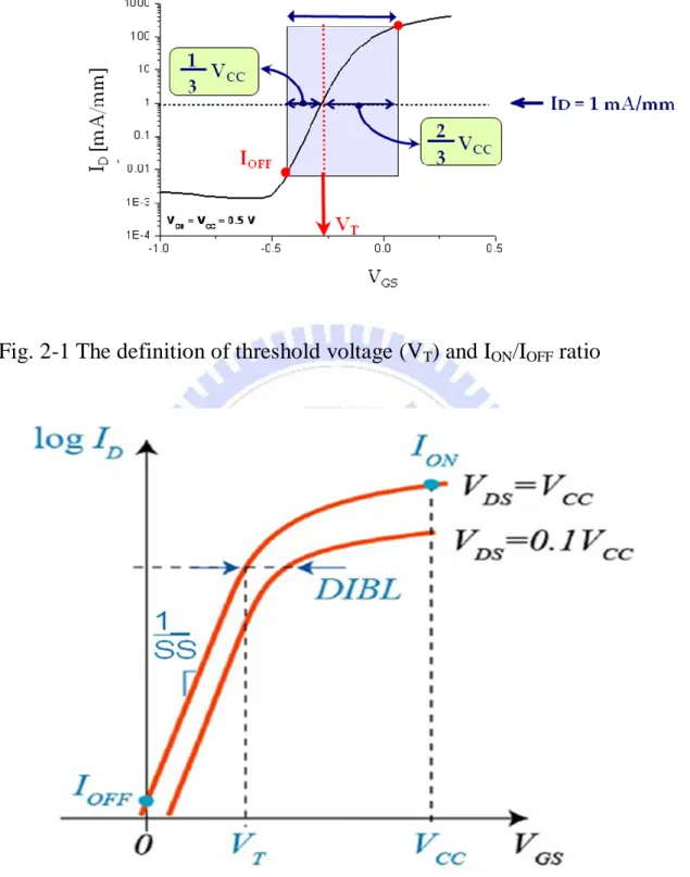
Owing to the high mobility and small energy band gap, InGaAs is widely used as the channel material to form hetero-junctions of HEMTs[3]. Accompanying with the Indium content of InGaAs increases, the electron mobility increases dramatically from 4600 cm2V-1S-1 (In: 0%)
to 20000 cm2V-1S-1 (In: 100%) at 295K. Meanwhile, the energy band gap decreases, resulting in high gate leakage problem and low breakdown voltage. As the Fig.1-2 shows, the lattice constant increases as the band gap decreases, where also causes larger lattice mismatch with Silicon, leading to difficulty of integration between InGaAs and Si.
The logic suitability of InAlAs/In0.7Ga0.3As and InAlAs/InAs InP
HEMTs were estimated by D-H Kim et al., and high performance at low bias voltage (VDS=0.5V) for low-power logic applications were also
obtained[4]. Including subthreshold slope (S), drain-induced barrier lowering (DIBL) and ION/IOFF ratio, above figures of merit (FOM) which
are defined by Dr. Chau [1] are exhibited. However, further researches are of importance on solving the gate leakage problems, improving electrical characteristics and integrating III-V materials on silicon.
In this study, HEMTs with InGaAs channel of three different Indium concentrations (In0.22Ga0.78As, In0.7Ga0.3As and InAs) were fabricated to
investigate low-power logic suitability. In the first part,
InGaP/In0.22Ga0.78As pseudomorphic high electron mobility transistors
(PHEMTs) with various doping profiles were manufactured to identify the effects of doping profiles for RF and digital applications. In the second part, atomic layer deposition (ALD) Al2O3 will be introduced as
gate insulators for InAlAs/In0.7Ga0.3As metal-oxide-semiconductor
metamorphic high electron mobility transistors (MOS-MHEMTs) formation to solve the gate leakage problems. Finally, the fabrication of InAlAs/InAs/InP MOS-HEMTs employs air-bridge structure to develop several fan-out level devices. The RF and digital performances of HEMTs
3
1.2 Thesis Content
The contents of this thesis are composed of literature review, fundamentals of electrical characteristics, issue I~III, and conclusions. In Chapter 2, the literature survey on the HEMTs for digital applications and the fabrication of MOS-HEMTs are reviewed. In Chapter 3, the fundamentals of electrical characteristics are addressed. In Chapter 4, the brief introduction, experiment, results and discussion of issue I (digital and RF performance of HEMTs with different doping profiles) are described. In Chapter 5, the motivation, process flow, results and discussion of issue II (introducing ALD Al2O3 as gate insulator for
MOS-HEMTs fabrication) are discussed. In Chapter 6, the introduction, experiment, results and discussion of issue III (employing air-bridge structure on InAs MOS-HEMTs for digital applications) are exhibited. Finally, the conclusions will be given in Chapter 7.
Fig. 1-1 Cutoff frequency versus power dissipation curves of HEMTs and Si-MOS
Fig. 1-2 Energy band gap versus lattice constant diagram of III-V
materials 101 102 103 0 100 200 300 400 101 102 103 0 100 200 300 400 Cutoff Frequ enc y , f T [GH z] Power Dissipation [mW/mm] Buried Pt on InAlAs (V CC = 0.5 V) Si NMOS (L g= 80 nm, VCC= 0.7 V) Lg= 100 nm L g= 50 nm
5
Chapter 2 Literature Review
2.1 HEMTs for digital applications
The alternative devices of Si MOSFET for digital applications are researched because the Si technology roadmap is expected to come to the end. III-V material HEMTs are the potential candidates due to superior device performance as mentioned in the former chapter.
Recently, the 40nm InAs HEMT and the In0.7Ga0.3As HEMT which
have been fabricated by Dae-Hyun Kim and Jesús A. del Alamo exhibit impressive results for high-performance low-power application[2.4]. The 100nm In0.7Ga0.3As HEMTs yield drain induced barrier lowering (DIBL)
as low as 80 mV/V, subthreshold slope (S) of 77 mV/decade, and ION/IOFF
ratio in excess of 103 with a gate delay of about 1.2 ps. Moreover, the 40nm InAs HEMTs demonstrate DIBL = 80 mV/V, S = 70 mV/decade, ION/IOFF ratios in excess of 104 and fT= 475 GHz. These remarkable results
imply that InAs is a material with great potential for beyond Si CMOS logic applications.
The high performance of the HEMTs could be summarized to optimize the following three parameters. One is the gate length. The shrink of gate length leads to higher Gm and cutoff frequency. Another is
the gate-to-channel thickness. Thinner insulator devices exhibit more positive VT, higher current drive and better short channel effects, such as
lower output conductance, less DIBL and sharper subthreshold slope. The other parameter that has to be moderated is the lateral recess length which
is the effective factor of gate-to-drain capacitance (CGD). The optimized
lateral recess length is 150 nm.
2.2 Logic parameters for low-power application
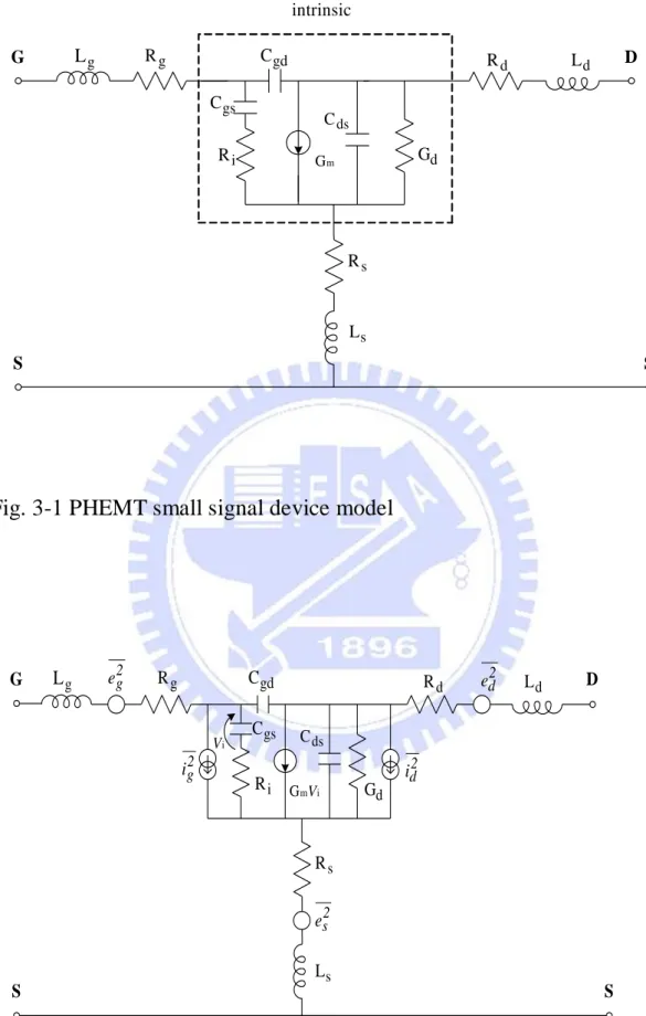
The calculating methods of the logic parameters, including subthreshold slope (SS), drain-induced barrier lowering (DIBL), ION/IOFF ratio and gate delay time, above figures of merit (FOM) are
defined by Dr. Chau[2]. The bias point is set at VDS=0.5 volt. The ION/IOFF
ratio can be defined as the following. First, we defined the threshold voltage as the value of VGS for which the drain current is 1 mA/mm at
VDS = VCC. Then, we selected ION as 2/3 VCC above VT, and IOFF as 1/3
VCC below. The above methodology is displayed in Fig. 2-1.
The definition of the subthreshold slope (SS) and drain-induced barrier lowering (DIBL) are illustrated in Fig. 2-2. The steepness of the transition between the on and off states is evaluated through the SS. The smaller magnitude of SS means one can apply less gate voltage to control the on and off current. The tightness of the threshold voltage is evaluated by DIBL, which measures the change in VT as a result of a change in VDS.
If DIBL is small, VT is insensitive to manufacturing circuit design.
Finally, the gate delay time is of importance to evaluate the response time of gate. The following formula gives the estimating equation, where C is total gate capacitance, which could be calculated by measuring high frequency S-parameters.
7
2.3 MOS-HEMTs fabrication
Owing to the high performance of the above devices, InAs HEMT is expected to be the most potential candidate for the next generation technology[5]. However, the small band gap of InAs channel leads to the impact ionization between gate and grain, and the Schottky gate also suffers from gate leakage problem. Therefore, the insulating layer is introduced to solve the problem, including high aluminum content native oxide of InAlP or InAlAs[6], ALD high-k dielectrics such as Al2O3[7] and
HfO2[8].
2.4 Surface treatment
Surface treatment is of importance to be handled before applying the insulating layers to restrain interface trap density which would cause the undesired Fermi level pinning of the carriers. Several surface treatment solutions have been exhibited with high capability of passivation, such as HCl, NH4OH and (NH4)2SX. The devices treated by NH4OH and
(NH4)2SX reveal compatibility between the oxide layer and
semiconductor[9].
Fig. 2-1 The definition of threshold voltage (VT) and ION/IOFF ratio
Fig. 2-2 The definition of subthreshold slope (SS) and drain induced barrier lower (DIBL)
9
Chapter 3
Fundamentals of Electrical
Characteristics
For devices used in high frequency operation, we need to consider the operation frequency, linearity, power density, power efficiency, and noise figure. In this chapter, the correlation of the device performance with the device structure used will be discussed. These include the improvement of device breakdown voltage, noise figure, linearity, and fT,
fmax based on the improved design of the device structure.
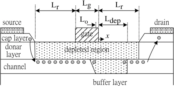
3.1 Device model
PHEMT developed is characterized using on-wafer probing and the bias-dependent S-parameters are measured and followed by equivalent circuit parameter extraction. The small-signal equivalent circuit (Figure 3-1) used for parameter extraction also requires “cold measurement” (Vds=0). The cold measurement data are used to estimate the value of the
parasitic elements following the procedures proposed by Berroth and Bosch for MESFETs.
As shown in Figure 3-1, the symbols for the device parameters could be explained as following.
(a) Cgs:the capacitance between gate and source has the expression.
where Cgsi is an intrinsic component which for a given Lg is proportional
to 1/Dg, and Cgsf is a fringing capacitance which is an additional parasitic
capacitance. Dg is gate-to-channel distance, and Cgs is expected to be
proportional to 1/Dg and increases with recess depth. The magnitude of
Cgsf is relatively small compared to the intrinsic Cgsi value [3].
(b) Cgd:the capacitance between gate and drain is given as:
Cgd = Cgd,dep + Cgd,met = Cgdi + Cgdair + Cgdsc
Cgd,met is the feedback capacitance due to the gate-drain metallization
depending on the gate-to-drain distance. Cgd,dep is the feedback
capacitance due to the gate-drain depletion [4].
In another expression, Cgd is a parasitic capacitance between gate and
drain, and it consists of three terms: Cgdi (the capacitance of the gate-drain
surface depletion region), Cgdair (a weak contribution through the air), and
Cgdsc (an intrinsic component due to the short channel effect). By a deeper
recess, Cgdi and Cgdair decrease due to lateral extension of the recess notch.
Cgdsc, on the other hand, increases due to the reduced short channel effect.
Since the later effect is important for shallow recess, the overall Cgd
characteristics show first a slow rate of decrease in capacitance with recess and later on a much faster rate of decrease, and the ratio of Cgs and
Cgd increases with deeper recess [3].
(c) Ri:the series resistance between gate and drain
(d) Gd:the conductance between drain and source
11
(f) Lg:the inductance of the gate metal
(g) Rg:the resistance of the gate
(h) Gm:transconductance
(i) Rs:the resistance of the sum of gate-source intervening material and
the ohmic contact of the source electrode.
(j) Ls:the inductance of the sum of gate-source intervening material and
the ohmic contact of the source electrode.
(k) Rd:the resistance of the sum of gate-drain intervening material and the
ohmic contact of the drain electrode.
(l) Ld:the inductance of the sum of gate-drain intervening material and
the ohmic contact of the drain electrode.
3.2 Noise figure (NF)
In wireless communication, the generation of noise will affect the quality of the signal transmission. The transferred signals cannot be discriminated if the noise disturbance is too large. There are many different types of noise generation, and the two most influential of them are “thermal noise” and “shot noise”. In real amplifiers, thermal noise consists of the resistance in circuit, the electrode impedance of the transistor, and the resistance of the semiconductor layer. Shot noise is due to the electron migration. The equivalent circuit with noise source is shown in Figure 3-2.
According to the Nyquist theorem, the effective noise power Pnav in
the bandwidth Δ f can be expressed as:
Pnav=kTΔ f
where k is the Boltzmann’s constant, and T is the absolute temperature. If
we show with noise voltage:
2
e =4kTRΔ f
Therefore, the source resistance Rs, gate resistance Rg, and the drain
resistance Rd would generate resistance thermal noise
2 s e , 2 g e , and 2 d e . The noise figure can be expressed as [5]:
m s g i T f mim G R R K f f K F 1 ( ) (1)
3.3 Linearity
Linearity of amplifiers is often assessed by the third-order intercept point (IP3). If an amplifier is presented with two signals closely spaced in frequency, and a perfectly linear amplifier would simply amplify the two signals. However, the real amplifier is never with perfectly linearity, and nonlinearity will result in additional output signals. A nonlinear amplifier will have a transfer function that can be approximated as:
Po = a1Pin + a2P 2
in + a3P 3
in + … (2)
where Pin and Po are the input and output power, and ai are coefficients. A
13
two closely spaced frequencies, f1 and f2:
Pin = P1sin(2π f1t) + P2sin(2π f2t) (3)
If Eq. (3) were substituted into Eq. (2), we can use elementary algebra and trigonometric identities to show that the output power (Po)
contains the following components: t f P a1 1sin21 t f P a1 2sin2 2 (fundamentals) t f P a sin2 (2 ) 2 1 1 2 1 2 t f P a sin2 (2 ) 2 1 2 2 2 2 (second-order products) t f f P P a sin2 (2 ) 4 3 2 1 2 2 1 3 t f f P P a sin2 (2 ) 4 3 2 1 2 2 1 3 (third-order products)
Assuming P1 = P2, second-order product power is proportional to the
square of the input signal power, third-order product power is proportional to the cube of the input signal power, and so on. But only the odd and greater than third-order terms have greater attribution to the fundamental signal. So we usually consider the fundamental signal and the third-order product signal only. Figure 3-3 is the output power diagram of the fundamental and the third-order product signals. From Figure 3-3, we can identify the third-order intercept point (IP3). The Pin
value of IP3 is also called IIP3, which is important for low noise amplifier. From the fundamental diagram of microwave front-end device (Figure 3-4), the low noise amplifier is used to receive signals. So a higher IIP3
value results in a higher linearity of the amplifier, and the less distortion of the input signals.
3.4 Breakdown voltage (BV
gd)
3.4.1 Physics for device breakdown
Breakdown in HEMT devices may result from many effects, such as avalanche multiplication, thermionic or thermionic-field emission across the insulator, and electron tunneling through the insulator, which is also referred to as “impact ionization” at a potential step. The insulator contains Schottky layer and channel layer, and the impact ionization mechanism consists of two steps. First, electrons are injected by thermionic field emission from the gate to the insulator. Second, because of the large conduction band offset and the electron field in the insulator, these hot electrons enter into the high field gate-drain region of the channel. Then the electrons immediately relax their energy through impact ionization.
For the InAlAs/n+-InGaAs HEMT, the off-state breakdown voltage increases with lower InAs mole fraction in the insulator and enhanced channel bandgap (by quantum size effects in thin channels). The insulator with lower InAs content has a larger schottky barrier height, and enhances breakdown by suppressing thermionic emission. Besides, increase in channel bandgap (by quantum size effects) also increases breakdown voltage by suppressing impact ionization [6].
15
Different kinds of devices may suffer from different breakdown mechanisms, depending on the details of the design such as insulator thickness, recess, and channel composition. Breakdown voltage also shows a negative temperature coefficient. The channel electrons heated by the lateral electric field give rise to impact ionization and light emission. We were able to identify two main different light emission mechanisms. They are conduction band to conduction band transitions for low energy photons, and conduction band to valence band transitions for high energy photons. The correlation between the gate current and the light intensity allowed us to separately evaluate the electron and hole components of the gate current.
For InAlAs/InGaAs heterostructure FET, the gate current at room temperature is strongly influenced by Real Space Transfer (RST) of both hot holes and electrons across the InAlAs barrier. According to the Id vs.
Vds curve, the negative gate current reaches a maximum when Vgs=0V
and then decreases by increasing the gate voltage toward negative values. This increase in the gate current is due to the RST and collection of holes generated by impact ionization at the drain end of the channel, where the maximum electric field occurs [7].
The gate-to-drain breakdown voltage BVgd is defined as the
gate-to-drain voltage when the gate current is 1mA/mm.
3.4.2 Analytic model for design
HEMT with the depletion region near the gate electrode at the saturation region. The gate is assumed to be formed symmetrically between drain and source electrodes, and the channel is to be depleted between the gate and drain because of drain-gate voltage Vgd. The length of the depletion
region between the gate and drain is denoted as Ldep.
From Figure 3-5, the lateral electrical field in the channel Ech can be
obtained by assuming that all electric field lines associated with lateral spreading of the depletion region terminate over some distance L0 along
the gate metal. This assumption was proposed by Wemple et al. to describe the breakdown voltage of GaAs-based MESFETs with a recessed gate, and the breakdown phenomena can also be successfully explained using this assumption. This assumption was applied to a HEMT structure to describe the breakdown. The distance L0 plays a roll in the
adjustable parameter of the model but not in L0<<Lg. The lateral electrical
field in channel Ech is obtained by applying Gauss’s law to the geometry
of Figure 3-5. 0 L x qn E s ch (4) where x is the coordinate along the gate, the origin of which is at the edge of the gate, ε is the dielectric constant of material of the channel, and ns
is sheet carrier concentration in the channel.
The breakdown voltage BVgd can be defined as the gate-to-drain
voltage when Ech is equal to avalanche electric field Ea. If the distance xb
where Ech is equal to Ea where smaller than Lr, BVgd can be defined and
17 s a gd qn E L BV 2 2 0 when xb< Lr (5)
where the voltage drop between the gate and drain is assumed to mainly occur in the depletion region. Using this assumption, the length of the depletion region Ldep can be obtained by integrating Eq. (4) with respect
to x from 0 to Ldep. gd s dep V qn L L 2 0 (6)
The depletion region spreads with Vgd and the breakdown phenomena
occur when Ldep is equal to xb. Note that the expression of BVgd in Eq. (5)
means that the breakdown voltage is not improved by widening the gate recess region and it is determined by only the structure of the epitaxial layers.
Figure 3-6 shows the dependence of the breakdown voltage BVgd on
the width of the gate recess. They can be calculated by using a simple model that was already described before. The calculated breakdown voltage increased with the width of gate recess and then saturated. This tendency was also confirmed experimentally [8].
3.4.3 Improvement of the breakdown voltage
In the off state, the gate leakage current is generally attributed to a two-step process. First, impact ionization in the channel creates electron-hole pairs. Second, the resulting holes reach the gate where they are collected, thus generating an excess leakage current. Consequently, two parameters are of a prime importance on the high voltage behavior of
the HEMTs. They are the band-gap (Eg) of the channel material that
mainly determines the impact ionization rate, and the energy barrier seen by the holes created in the channel (EB) in their path toward the gate. In
order to prevent this leakage, several improvements of the structure design were proposed which all tend to either minimize the ionization mechanism in the small band-gap InGaAs channel or to increase the holes barrier. There are several methods to decrease the leakage current and improve the breakdown voltage, which are described as following.
(a) The reduction of the channel thickness leads to a larger gap by quantization effects.
(b) A suitable channel design reduces the electric field in the channel. (c) An Al-rich InAlAs spacer or an InGaP spacer increases the hole
barrier [9].
(d) Different gate metal will lead to different barrier height.
(e) Mesa sidewall etch will reduce the gate leakage current and improve the breakdown voltage.
InAlAs/InGaAs HFETs fabricated by conventional mesa isolation have a potential parasitic gate leakage path where the gate metallization overlaps the exposed channel edge at the mesa sidewall. The parasitic gate leakage path is formed by the low Schottky contact of the exposed channel edge with the gate metallization. It has been proven that the existence of this path by fabricating special heterojunction diodes with different mesa sidewall gate metal overlap lengths. The sidewall leakage current is a function of the crystallographic of the sidewall, and increase with channel thickness, sidewall overlap area, and InAs mole fraction in
19
increased the subthreshold and forward gate leakage currents, which will lead to the reduction of the breakdown voltage [10].
3.5 Extrinsic transconductance (g
m)
The transconductance of the HEMTs indicates the ability of the gate voltage on the control of the drain current. It can be defined as:
(7)
where the vsat is the electron velocity of the “two dimensional electron
gas” (2-DEG).
The measurement requires specification of the initial gate voltage, the gate voltage step, and the drain voltage at which the measurement is made. Because of the nonlinear behavior of source-drain current as a function of gate voltage, gm typically will become less as the bias
approaches pinch-off approaches. This also means that a smaller voltage step will yield a higher transconductance. The extrinsic transconductance is a function of the total gate width of the device, so the width must also be given. Besides, gm may also be normalized to a unit gate width, usually
mmho/mm.
3.6 Unit current gain cut-off frequency (f
T) and maximum
frequency of oscillation (f
max)
sat G G D m Z v d dV dI g 2 2
The intrinsic device model for the HEMT device is shown in Figure 3-7. If we only consider the intrinsic part, the current can be expressed as: ' 2 ' 22 ' 1 ' 21 ' 2 ' 2 ' 12 ' 1 ' 11 ' 1 V y V y i V y V y i (8)
assume (ωCgsRi)2 << 1, then we can get:
) ( ) ( ) ( ) ( ) ( 2 2 ' 11 ' 21 ' 1 ' 2 ' 22 ' 21 ' 12 2 2 ' 11 gd gs i gs m i gs gd m ds gd d m gs gd m gd gd gs i gs C C j R C G R C C j G y y i i C C j G y G C C j G y C j y C C j R C y (9) assume i gs gd gs m i gs gd m R C C C G R C C G 2 2 ) ( | ) ( |
fT is defined as the frequency when current gain ' 1
1 ' 2 i i , and can be expressed as: ) ( 2 gs gd m T C C G f (10)
fmax can be obtained by using unilateral gain:
d i T d i gs m U G R f f G R C G f y y y y G U 1 4 1 1 ) 2 ( 1 4 1 ) Re( ) Re( 4 | | 2 2 2 2 ' 22 ' 11 2 ' 12 ' 21 max (11)
21 d i T G R f f 2 max (12)
If we further consider gate resistance Rg, ohmic contact resistance Rs
and Rd, then the small signal equivalent circuit is shown as Figure 3-8.
assume (CgsRi)2 1 i gs gd gs m i gs gd m R C C C G R C C G 2 2 ) ( | ) ( | Gm |Gd j(Cgd Cds)| then |Y'| y11'y22' y12'y21' jCgdGm Transfer y parameter into Z parameter:
s d s s s g R R Y y Z R Y y Z R Y y Z R R Y y Z | | ' | | ' | | ' | | ' ' 11 22 ' 21 21 ' 12 12 ' 22 11 and |Z|Z11Z22Z12Z21
gs gd d gd m
s d gd gs m m gd ds gd d gd gs s d gd gs m gd ds gd d gd gs s m s d s G C j G C C j R R C C j G i i G C j C C j G C C j R R C C j G C j C C j G C C j R G Y R R y Y R y Z Z Z Z y y i i )] ( [ ) ( ) ( )] ( )][ ( [ ) ( ) ( )] ( )][ ( [ | | ) ( | | | | | | 1 2 11 21 22 21 11 21 1 2
( )[1 ( ) ] ( ) 2 gs gd d s d gd m d s m T R R G C G R R C C G f (13)2 max ) 1 )( 5 . 2 1 ( 5 4 ) / 1 ( 4 m s gs gd gs gd s m g s i m m d T R G C C C C R G R R R G G G f f (14)
fT and fmax are parameters often used to indicate the high frequency
23 G D S S intrinsic d R Ld d G ds C Gm i R gd C gs C g R g L s R s L
Fig. 3-1 PHEMT small signal device model
G D S S GmVi Vi 2 d i 2 d e 2 g i 2 g e 2 s e g R g L Cgd gs C ds C d R d G s R d L i R s L
-30 -25 -20 -15 -10 -5 0 5 10 15 -120 -100 -80 -60 -40 -20 0 20 40 60 3rd ORDER PRODUCTS FUNDAMENTALS
3rd ORDER INTERCEPT POINT
OP1dB OIP3 Outpu t Powe r (d Bm) Input Power (dBm)
Fig. 3-3 Output power diagram of fundamental andthird-order product signals Duplexer Antenna fRF fIF fLO
LNA Filter Mixer IF amplifier
Signal process circuit Modulator PA Pre-amplifier LO
25
Fig. 3-5 A schematic cross-section of the InAlAs/InGaAs PHEMT
Fig. 3-6 Dependence of the breakdown voltage (BVgd) on the gate recess
width
buffer layer
depleted region
gate
source
drain
channel
cap layer
donar
layer
g
L
r
L
r
L
dep
L
oL
x
0.0 0.1 0.2 0.3 0.4 0.5 0.6 0 3 6 9 12 15 BV gd ( V) Lr (um)G'
D'
S'
S'
V
1'
V
2'
gs mV
G
dsC
dG
gsC
gdC
iR
gsV
I
2'
'
I
1Fig. 3-7 PHEMT intrinsic device model
G
D
S
S
gR
C
gd gsV
1I
1V
iR
gsC
dsC
dG
dR
2I
gs mV
G
2V
sR
27
Chapter 4
RF and Digital Performance of
HEMTs with Different Doping
Profiles
4.1 Introduction
For high frequency wireless communication, as the density in information traffic increasing, the requirements of device linearity become more demanding. In addition, the device linearity could be improved by varying the doping profiles. The device linearity of InGaP/InGaAs HEMTs with different doping profiles will be discussed in this chapter.
InGaP/In0.22Ga0.78As pseudomorphic high electron mobility
transistors (PHEMTs) have been widely discussed for the radio frequency (RF) applications[10-12]. Unlike general AlGaAs Schottky layer forms a deep-complex (DX) center at the desired doping level, wider band gap InGaP presents better insulating property. Moreover, the high etching selectivity between InGaP and GaAs can be achieved, which improves the uniformity of gate recess[13].
For digital applications, endowed with smaller lattice constant compared to In0.7Ga0.3As and InAs, In0.22Ga0.78As displays relatively
higher possibility to integrate with Silicon. Due to the lower mobility of In0.22Ga0.78As, various doping methods are employed for performance
reinforcement.
4.2 Device Fabrication
The epitaxial layers of the InGaP/In0.22Ga0.78As PHEMTs were
grown by metal-organic chemical vapor deposition (MOCVD) on GaAs substrate along the (100) axis. The schematic cross-sectional view of our InGaP/In0.22Ga0.78As HEMT structure with various doping profiles are
shown in Fig. 4-1~4-3.
Fig. 4-1 shows the illustration of δ-doped InGaP/In0.2Ga0.78 As
HEMT which consists of , from bottom to top, GaAs buffer layer, AlGaAs barrier layer, δ-doped carrier supply layer with Si doping concentration of 4.0×10¹²/cm2 which provides carriers, AlGaAs spacer
layer, δ-doped carrier supply layer, InGaP Schottky layer and n-GaAs cap layer with Si doping concentration of 3.0×10¹²/cm3. It is worth noticing
that the upper barrier material is InGaP which is different from the lower AlGaAs. The former has wider band-gap leading to higher breakdown voltage, and the later AlGaAs/InGaAs hetero-junction causes higher gm
value than that with InGaP spacer.
Fig. 4-2 exhibits the structure of InGaP/In0.22Ga0.78As HEMT with
uniformly-doping profile which indicates the carriers are doped in the Schottky layer. Other layers are as the same as the δ-doped for
comparison. Fig. 4-3 shows the diagram of channel-doped
InGaP/In0.22Ga0.78As HEMT. The carriers are supplied by Si δ-doped
29
The detailed manufacturing process on the InGaP/In0.22Ga0.78As
HEMT devices are described at the following sections. Besides, the three kinds of devices HEMTs were fabricated by the same process flow for comparison. The flow chart of the process for device fabrication is illustrated in Fig. 4-4.
4.2.1 Wafer cleaning
The purpose of wafer cleaning is to remove undesirable impurities and particles on the surface. The wafers were immersed in Acetone (ACE) and isopropyl alcohol (IPA) each for five minutes, and blown dry by nitrogen gas.
4.2.2 Mesa isolation
The active region of devices is defined by S1818 photoresist, and other potions were wet etched to the buffer layer. The mesa isolation was carried out by HF:H2O2:H2O (5:1:40) solution to etch the GaAs cap layer,
and HCl:H2O (1:1) solution to etch the InGaP Schottky layer. Then, the
etching depth will reach about 4000Å by utilizing HF:H2O2:H2O solution
again. The etching depth is measured by α-step measurement.
A low contact resistance junction is formed between the ohmic metal (Au/Ge/Ni/Au) and the cap layer, where germanium is used for doping GaAs during alloy, and nickel acts as a wetting agent in order to prevent the AuGe metal from “balling up”.
The ohmic contact region is defined by AZ5214E photoresist with undercut profile. The wafers are dipped in 20% HCl solution for 15 seconds to remove the native oxide. Ohmic metal was then deposited on the substrates by using an electron-beam evaporator at a pressure of ~1x10⁻⁶ Torr. After ACE lift-off procedure, the wafer was thermally
alloyed at 340℃ for 30 seconds by using rapid thermal anneal (RTA) system. After all, the contact resistance is obtained via measuring the transmission line method (TLM), and the specific contact resistivity is 1.9176×10⁻⁶ Ω cm2.
4.2.4 Recess and gate formation
The double gate recess process is used here.
The 1st recess slot was defined by e-beam photolithography to form the pattern defined by copolymer photoresist. Citric acid (C.A.) based solution (CA:H2O2:H2O) was used to etch the cap layer, and HCl based
solution (HCl:H2O) was used to etch the InGaP shottky layer until it
reaches the target current which was confirmed by measuring the drain-to-source current.
31
obtaining low gate resistance. In the T-gate structure design, the gate length is defined by the small footprint and the wide top offers low gate resistance.
After removing the 1st recess photo-resist, the gate openings are defined by e-beam lithography to form the T-shaped profile consisting of Copolymer/PMMA/Copolymer to obtain a T-gate. Then, the HCl based solution was used to execute the 2nd recess, which can further increase the breakdown voltage. After that, the wafers are dipped in the 20% HCl solution for 15 seconds to remove the native oxide fallowed by depositing Ti/Pt/Au by e-gun evaporation system, where Titanium provides good adhesion to substrate, platinum acts as a barrier to prevent gold diffusing into GaAs, and gold provides high electrical conductivity. Finally, the wafer was immersed into ACE to lift-off the undesired metal. As the result, the gate length of the InGaP HEMT in this chapter is 0.3μm.
4.2.5 Device passivation
In order to protect the devices from environmental contamination and mechanical damages, the silicon nitride film (SiNX) was formed by
PECVD. The wafer was first dipped in the solution of NH4OH:H2O=1:50
for 10 seconds to clean the surface and decrease the surface dangling bonds. The silicon nitride film was grown at 250℃. RF power was 35W, and the precursors were SiH4/Ar, NH3 and N2 . The film thickness was
about 1000Å and its refractive index was about 2.0, which were measured by ellipsometer.
After the passivation process, the contact via was defined for interconnections. Then the silicon nitride film was etched by reactive ion etching (RIE) system. The reactive plasmas are CF4 and O2, the RF power
is 80W, and the pressure is 60 mtorr.
4.2.6 Air-bridge plating
Electrical plating is usually the last major step of the front-side process, and plated air-bridges are commonly used in GaAs devices and MMICs to interconnect source pads of the HEMTs.
First, a layer of photo-resist was spun and patterned to open areas over metal pads. Then, a thin coating of Ti/Au/Ti was applied to the entire wafer, where Titanium is deposited to improve the adhesion. The thin metal layer can conduct the plating current to the whole wafer. Next, a second coating of photo-resist was applied and patterned. Then the wafer was electroplated with gold for 2μm thickness. After plating, the top resist layer, thin Ti/Au/Ti metal, and lower resist layer were removed individually, leaving only the plated air-bridge.
4.3 Results and Discussion
33
Three different types of 0.25μm × 160μm InGaP/InGaAs HEMTs are shown in Fig.4-1~4-3 were fabricated, tested and compared. Fig. 4-5 shows the IDS vs. VDS curves of the three different types of devices. For
Comparing these devices, those different types devices have designed with similar IDSS (IDS @ VGS = 0V) and pinch off voltage. The
characteristics of the Gm dependence on the gate bias are shown in Fig. 4-6(a). It can be observed that extra doping in the channel and using uniformly-doped will result in device flatter Gm distribution, but both have lower maximum Gm value as compared to the conventionalδdoped device. The IDS-VGS curve comparison of these devices is shown in Fig.
4-6(b). The channel doped device has a maximum IDS value of
634.3mA/mm which is higher than the others. The DC characteristics of these three 0.25 um × 160 um devices are compared in Table I.
To evaluate the device linearity, IP3 of these devices were measured. The IP3 measurements were carried out by injecting two signals with the same amplitude but at two different frequencies: 5.8 GHz and 5.801GHz, with the devices biased at VDS = 1.5V, and adjust the IDS to get the IP3 vs.
IDS curve. Fig. 4-7 shows the IP3 versus IDS curves of these three different
power for each individual device. It shows that the channel doped and uniformly-doped devices have higher IP3 values. The uniformly-doped devices device has wider high IP3 region versus different IDSThe
measured maximum IP3 of these devices are listed in Table 5-2. The tuning at Γsource and Γload of the conventional δ doped, uniformly-doped
and channel doped devices are Γsource = 0.50∠56.7 o
, 0.05∠-176.17o, and
0.02∠-83.6o and Γload = 0.14∠47.1 o
, 0.58∠32.3o and 0.51∠56.0o
respectively. The uniformly-doped device shows higher IP3 of 22.19 dBm, and the channel doped device shows higherΔ(IP3-P1dB) of 14.23 dB, and
higher IP3 to DC power consumption ratio (IP3/PDC) of 4.97 compared to
other devices. Overall, the uniformly doped and channel doped device has higher value of figure of merit for device linearity. From the data in Fig.4-6 and Fig.4-7, it can be concluded that extra doping in the channel region or using uniformly-doped can achieves flatter Gm distribution versus VGS bias and thus higher IP3 of these devices even though the
conventional δ doped device exhibits higher peak Gm value.
4.3.2 Devices for Logic applications
For better logic performance, the reduction of gate-to-channel distance is of importance, and further recess is required to reduce the
35
depth. Electrical characteristics of the 0.3μm InGaP/In0.22Ga0.78As
PHEMTs with three different structures are plotted in Fig. 4-1~4-3 and analyzed under the bias condition that drain-to-source voltage (VDS) is
equal to 0.5 volts. Extrinsic transconductance (Gm) versus gate-to-source
voltage (VGS) curves are displayed in Fig.4-8. Among the devices,
although the δ-doped one shows the highest peak Gm of 308 mS/mm, the
uniformly-doped one exhibits positive shift in the threshold voltage, leading to lower power dissipation. The peak Gm of channel-doped one is
compressed due to lightly doping in the channel.
Fig. 4-9 presents the subthreshold characteristics of the manufactured InGaP/In0.22Ga0.78As PHEMTs at a VDS of 0.5volts. The
lowest off-state current is determined by the gate leakage current, which indicates the well insulating property of the δ-doped device. It is worth noticing that the uniformly-doped device reveals sharpest subthreshold slope, contributing to better logic performance.
The gate leakage current and the breakdown voltage diagram are illustrated in Fig. 4-10 and 4-11. Due to the good insulating property, the δ-doped InGaP/In0.22Ga0.78As device displays high gate-to-drain
breakdown voltage (BVDG) is 15 volts and low leakage current density of
10-4 mA/mm, which reaches the acquirements of logic gate (about 10-10
A/device). In addition, the BVDG of the uniformly-doped and
channel-doped devices are 7.4 and 4.8 volts, respectively. Further insulating improvement are needed to reinforce for these two kinds of doping methods.
Table 4-3 lists the logic parameters of the three InGaP/In0.22Ga0.78As
the chapter 3 exhibits and measured at a VDS of 0.5volts. In comparison
with the δ-doped device, on the one hand, uniformly-doped device shows smaller subthreshold slope (SS) of 111mV/decade and higher ION/IOFF
ratio where implies that uniformly doping in the Schottky layer could sharpen the VG-ID curve; on the other hand, channel-doped device
presents smaller drain induced barrier lowering (DIBL) of 78 mV/V where manifests that extra doing in the channel could help devices working at low bias point.
4.4 Conclusions
Electrical characteristics of the 3μm InGaP/In0.22Ga0.78As PHEMTs
with different doping profiles for low-power digital applications are illustrated. The δ-doped InGaP/In0.22Ga0.78As device presents possible
large scale integration of devices, attributing to the well insulating properties. In addition, SS and ION/IOFF ratio parameters can be improved
by uniformly-doping in the Schottky layer; DIBL parameter can be reinforced by extra doping in the channel layer. However, further insulating layer should be applied to the uniformly-doped and channel-doped devices for preventing them suffering from the gate leakage problem.
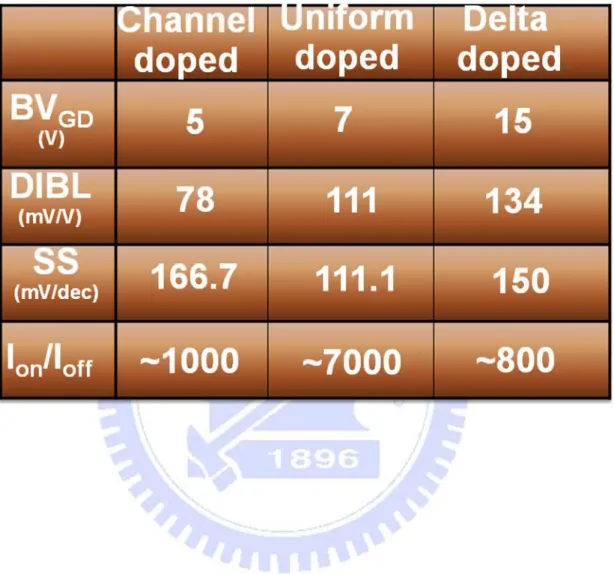
37
Table 4-1 Comparison of the DC characteristics of the three different types of devices Device Type Conventiona lδdoped InGaP/InGa As PHEMT Channel doped InGaP/InG aAs PHEMT Uniformly doped InGaP/InG aAs PHEMT Dopi ng dens ity Delta doping (cm-2) abo ve 4.0×10¹² 4.0×10¹² undoped bel ow 2.0×10¹² 2.0×10¹² Channel doped (cm-3) undoped 5.0×10¹⁷ undoped Uniformly doped carrier layers (cm-3) abo ve undoped undoped 3.0×10¹⁸ bel ow 2.0×10¹⁸ IDSS (IDS @ VGS=0, mA/mm) 356.9 359.6 361.0 IDS-max (mA/mm) 509.3 634.3 589.9 Gmmax (mS/mm) 372.1 368.4 340.0 Pinch-off voltage -1.25 -1.35 -1.4
Table 4-2 Comparison of the IP3 of the three different types of devices
Device Type DC bias point: VDS = 1.5V IDS (mA) Operation frequency: 5.8GHz P1dB (dBm) IP3 (dBm) Δ (IP3-P1dB) (dB) IP3/PDC Conventional delta-doped InGaP/InGaAs PHEMT 22.34 5.79 17.38 11.59 1.63 Uniformly- doped InGaP/InGaAs PHEMT 22.48 9.69 22.19 12.5 4.91 Channel doped InGaP/InGaAs PHEMT 16.96 6.79 21.02 14.23 4.97
Table 4-3 Logic parameters of the 0.3μm InGaP/In0.22Ga0.78As PHEMTs
39
Fig. 4-1 Structure of δ-doped InGaP/In0.22Ga0.78As PHEMT
Fig. 4-3 Structure of channel-doped InGaP/In0.22Ga0.78As PHEMT
41 0.0 0.5 1.0 1.5 2.0 0 50 100 150 200 250 300 350 400 450 -1.2 -0.6 -0.8 -1.0 -0.4 -0.2 0 V GS (V): D ra in -Sou rce C u rre n t: I DS (mA /mm ) Drain-Source Voltage: (V) (a) 0.0 0.5 1.0 1.5 2.0 0 50 100 150 200 250 300 350 400 450 -1.2 -0.6 -0.8 -1.0 -0.4 -0.2 0 VGS (V): D ra in -Sou rce C u rre n t: I DS (mA /mm ) Drain-Source Voltage: (V) (b)
0.0 0.5 1.0 1.5 2.0 0 50 100 150 200 250 300 350 400 450 -1.2 -1.0 -0.8 -0.6 -0.4 -0.2 0 Dr a in -S o u rce Cu rr e n t: I DS (m A /mm ) Drain-Source Voltage: (V) VGS(V): (c)
Fig. 4-5 IDS vs. VDS curves for the three different types of 0.25 x 160
m2 devices: (a)δ -doped device, (b) Channel doped PHEMT,
43 -2.0 -1.5 -1.0 -0.5 0.0 0.5 1.0 1.5 0 100 200 300 400 500 G m ( m S/ m m ) V GS(V)
Conventional delta doped InGaP PHEMT Channel doped InGaP PHEMT Uniform doped InGaP PHEMT VDS = 1.5V (a) -2 -1 0 1 2 0 100 200 300 400 500 600 700 800 900 D ra in -So u rc e Cu rr en t IDS ( m A /m m ) Gate-Source Voltage VGS (V)
Conventional delta doped InGaP/InGaAs PHEMT Channel doped InGaP PHEMT
Uniform doped InGaP PHEMT V
DS = 1.5 V
(b)
Fig. 4-6 (a) Extrinsic transconductance (Gm) vs. VGS curves, (b) IDS vs.
VGS curves for the three different types of devices studied, the
10 20 30 40 50 12 14 16 18 20 22 24 26
Conventional delta doped InGaP/InGaAs PHEMT Channel doped InGaP PHEMT
Uniform doped InGaP PHEMT V DS = 1.5 V T h ir d o rd e r in te rc e p t p o in t: IP 3 ( d Bm ) (%) IDSS
Fig. 4-7 IP3 vs. IDS curves of the three 0.25x160μ m 2
InGaP/InGaAs PHEMTs in this study, the test frequency is 5.8GHz and VDS =
1.5V
Fig. 4-8 Extrinsic transconductance (Gm) versus gate-to-source voltage
(VGS) curves of the 0.3×200μm2 InGaP/In0.22Ga0.78As PHEMT
devices -2.0 -1.5 -1.0 -0.5 0.0 0.5 1.0 0 100 200 300 G M (m S /m m ) VG(V) InGaP/In 0.22Ga0.78As HEMT VD=0.5V , Lg=0.3m Delta-doped uniform-doped channel-doped
45
Fig. 4-9 Subthreshold characteristics of the 0.3×200μm2 InGaP/ In0.22Ga0.78As PHEMT devices
Fig. 4-10 Gate leakage current of the 0.3×200μm2 InGaP/In0.22Ga0.78As
PHEMT devices -2.0 -1.5 -1.0 -0.5 0.0 0.5 1E-5 1E-4 1E-3 0.01 0.1 1 10 100 1000 I D (mA/mm) V G(V) InGaP/In 0.22Ga0.78As HEMT V D=0.5V , Lg=0.3m Delta-doped uniform-doped channel-doped -1.5 -1.0 -0.5 0.0 0.5 1E-5 1E-4 1E-3 0.01 0.1 1 L eak ag e c u rr en t, I G ( m A /m m ) V G(V) InGaP/In 0.22Ga0.78As HEMT VD=0V &0.5V , Lg=0.3m Delta-doped uniform-doped channel-doped
Fig. 4-11 Gate-to-drain breakdown voltage (BVDG) of the 0.3×200μm2
InGaP/In0.22Ga0.78As PHEMT devices
0 3 6 9 12 15 0.0 -0.2 -0.4 -0.6 -0.8 -1.0 Leakage c ur rent, I G (m A /m m ) VD(V) InGaP/In0.22Ga0.78As HEMT Lg=0.3m Delta-doped uniform-doped channel-doped
47
Chapter 5
Introducing Al
2
O
3
as Gate Insulator
for InAlAs/In
0.7
Ga
0.3
As
MOS-MHEMTs Fabrication
5.1 Introduction
Considering HEMTs for digital applications, the InGaAs channel with high indium concentration is required for better performance and higher transconductance. Meanwhile, unlike the excellent insulating property of metal-oxide- semiconductor (MOS) structure in Si MOSFET, the Schottky gate in HEMT device suffers from high leakage current, which results in restricted input handling voltage. Furthermore, owing to this obstacle, these transistors could not be integrated in large scale. In order to reduce the gate leakage current, insulating layers were introduced into the gate formation, including high aluminum content native oxide of InAlP or InAlAs[6], ALD high-k dielectrics such as Al2O3[7] and
HfO2[8].
ALD Al2O3 is introduced in this study due to its relatively high band
gap (about 8.7eV) and remains amorphous under typical processing conditions. In addition, Al2O3 also performs high breakdown electric field
(5~20 MV/cm), high thermal stability (up to 1000℃) and strong adhesion with dissimilar materials[14]. With well-controlled thickness and uniform
Al2O3 layer deposited by ALD technology which employs surface
saturation reaction technique, ALD Al2O3 is the leading candidate for the
gate insulators in MOS-HEMT device. The comparison of other insulating material properties is shown in Table 5-1[15].
It is worth noticing that surface treatment is of importance to be handled before applying the insulating layers to restrain interface trap density which would cause the Fermi level pinning of the carriers. (NH4)SX is convinced as a useful surface treatment solution and both
Schottky capacitors and MOS devices are manufactured by several research groups[8, 13, 16]. Moreover, MOS-HEMT treated by (NH4)SX
have already been utilized for fabrication, which presents higher breakdown voltage and lower leakage current in comparison with conventional HEMTs[17].
In this study, we focus on the characteristics of the 0.8μm InAlAs/In0.7Ga0.3As MOS-MHEMTs with ALD Al2O3 as the gate
insulator and conventional HEMTs with the same structures will also be fabricated in order to make comparisons. Besides, including subthreshold slope (S), drain-induced barrier lowering (DIBL) and ION/IOFF ratio, above
figures of merit (FOM) for logic application will also be exhibited to realize the logic potential of MOS-HEMTs.