國立交通大學
材料科學與工程學研究所
碩士論文
以離子液體為模板劑所製備奈米孔洞低介電薄膜之
孔洞形貌與排列性質之探討
Pore Morphology and Ordering of Ionic Liquid Templated-TEOS
Nanoporous Low-k Thin Films
研 究 生: 蔡沁穎
指導教授: 呂志鵬 博士
以離子液體為模板劑所製備奈米孔洞低介電薄膜之孔洞形貌與排列性質之探討 Pore Morphology and Ordering of Ionic Liquid Templated-TEOS Nanoporous Low-k Thin
Films
研 究 生:蔡沁穎 Student:Chin-Ying Tsai
指導教授:呂志鵬 Advisor:Dr. Jihperng (Jim) Leu
國立交通大學 材料科學與工程學系
碩士論文
A Thesis
Submitted to Department of Materials Science and Engineering College of Engineering
National Chiao Tung University in partial Fulfillment of the Requirements
For the Degree of Master
In
Materials Science and Engineering
February 2012
Hsinchu, Taiwan, Republic of China
I 以離子液體為模板劑所製備奈米孔洞低介電薄膜之孔洞形貌與排列性質之探討 研 究 生:蔡沁穎 指導教授:呂志鵬 國立交通大學材料科學與工程學系碩士班
摘 要
為了解決孔洞型低介電材料在半導體後段製程後所遇到的可靠度與機械強度的問 題,而這些問題大都導致薄膜材料內部的孔洞太大,或者是孔洞分布不均勻所致。因此, 我們在起孔洞劑的選擇上朝向更小分子的需求日益明顯。本研究利用模板劑移除法藉由 在初始狀況中摻入小分子的起孔洞劑-離子液體 (Ionic liquid) 製備兩相均勻混合溶液, 經旋轉塗佈成膜後,最後以高溫燒除起孔洞劑而得到奈米孔洞低介電薄膜。在本研究中, 我們使用長鏈段型的離子液體 (C16mimI),因其擁有良好的雙親性,容易在系統中形成 微胞結構,再加上微胞結構的彼此靜電排斥力,使得起孔洞劑不會在溶劑揮發後,以及 之後的熱製程過程中發生聚集的現象而產生較大的孔洞。同時,也由於其良好的熱穩定 性使得離子液體適合我們應用在低介電後段製程中。 在儀器的鑑定上,我們使用熱重分析儀 (TGA) 來檢驗離子液體的熱裂解溫度 (thermal decomposition temperature)。利用紅外線光譜儀 (FT-IR) 來檢驗薄膜的化學結構。 孔隙率由 X 光反射儀 (XRR) 測得。利用掃描式電子顯微鏡 (SEM) 與穿透式電子顯微 鏡 (TEM) 來觀察孔洞形貌,並利用低掠角小角度 X 光散射儀 (GISAXS) 對孔洞形貌做 更進一步的檢驗,包括: 孔洞大小、孔洞間距、孔洞的排列性質等。 實驗結果顯示,長碳鏈型的離子液體 (C16mimI) 在做為模板劑,TEOS 為母體起始 結構的情況下,我們能得到性質良好的多孔性薄膜。在不同摻入比例起孔洞劑造成不同 孔隙率由小至大為 5.3%~41.1%的孔洞薄膜中,孔洞大小分布為 3.5~4.5nm,並展現狹窄 的孔洞分布。孔洞間距隨著起孔洞劑摻入比例增加而減少,從大到小為 8.0nm~4.5nm。II 從實驗結果我們進一步發現,在高摻入比例為 30%的孔洞薄膜中,其孔洞排列情形近似 於 2D hexagonal 的結構,顯示其孔洞分布有長程規則性。藉由不同熱處理溫度實驗的 探討,我們亦發現孔洞間距會受製程溫度影響,在高溫時因為薄膜厚度的收縮導致垂直 膜面方向的間距因而收縮。綜觀研究結果,說明了利用長碳鏈離子液體做為起孔洞劑不 會導致嚴重的孔洞聚集現象,對於孔洞大小能夠做有效的控制。以上研究將提供我們在 製備奈米多孔性低介電材料中選擇起孔洞劑的方向。
III
Pore Morphology and Ordering of Ionic Liquid Templated-TEOS Nanoporous Low-k Thin Films
Student: Chin-Ying Tsai Advisor: Dr. Jihperng (Jim) Leu
Department of Materials Science and Engineering National Chiao Tung University
Abstract
In order to circumvent the reliability issues encountered in integration of porous dielectric, a novel nanoporous low-k thin film using templating method is employed by introducing the ionic liquid to the silica matrix with well dispersed and discrete porogen to achieve excellent control of pore size and pore size distribution. In particular, long chain ionic liquid (C16mimI) was chosen due to its amphiphilic property, which can form electrorepulsive
micelle that would not aggregate during the drying of the as-deposited film by evaporation of solvent and further procedure of thermal curing, Also, the thermal stability at high temperature of ionic liquid make it suitable for low-k processing.
Furthermore, the properties of C16mimI templated low-k thin film were characterized by
various methodologies. First, the decomposition temperature by TGA to assure its feasibility to applied to the low-k materials. Second, the porosity created by the porogen removal is measured by XRR. Third, the GISAXS is a versatile technique to identify the structure information about pore morphology including pore size, pore size distribution, pore ordering. Also, the TEM provide the visualization of the pore structure to see the nanoporous clearly compared to GISAXS. It was found that long chain ionic liquid behave as a promising template to the silica matrix to prepare such a nanoporous low-k thin film with various
IV
porogen loading. In the relatively high porogen loading (30%) leading to high porosity (~41.1%), the pore size is 3.5nm and regular pore spacing was ~5nm with uniformly distributed pore structure and no further aggregation of porogen molecule occurred. Besides, the pore spacing could be affected by the thermal curing temperature due to the film shrinkage effect. In summary, we have made a preliminary study and offered a better porogen selection in making a nanoporous thin film templated by ionic liquid.
V
誌 謝
首先,我要誠摰的感謝我的指導教授,呂志鵬博士。謝謝老師在日常生活中給予的 幫助,以及在研究以及實驗上給予的諄諄教誨,帶領我進入半導體以及低介電材料的領 域。從化學轉到材料領域的途中遇到過一些困難,謝謝有老師這一路上的協助。 碩士班的日子其實說長不長,說短不短,但在人生中實是一段寶貴的經驗,在這一 小段旅程中,我要感謝實驗室的學長姊們、同學們、以及學弟妹陪我走過這段路,你們 都給過我不少幫助,特別是在我需要你們的時候,衷心的感謝你們。 感謝國原學長在我剛進實驗室時不時的提供寶貴的意見;感謝幸鈴學姊在題目的選 擇以及化學方面的給予過的幫助,每次與你討論都很有收獲;感謝牧龍、昱涵、弘恩學 長、詩雅學姊在 low-k 方面的細心指導,你們在我的實驗及研究上幫助我很多;謝謝明 義、王智學長,雖然不同領域,但你們也給過我不少的建議或方向;謝謝伯政、瑜修學 長、琬婷學姊,在我剛進碩班時,你們幫助我熟悉實驗室的一切讓我們幾個同學們倍感 溫馨:奎岳、書豪、勝翔,你們是最好的同學,不管是打屁聊天、運動、玩樂、爬山, 都少不了有你們的回憶;也要謝謝最好的學弟妹們:丞芳、維剛、雅婷,祝你們實驗順利, 早日畢業。 感謝我的家人們,在我碩士生涯裡悉心地照顧;也謝謝我的女朋友瑜珮的體諒與包 容,在最後的階段,你的鼓勵對我來說真的很有用。 最後我要感謝國科會(計畫編號 99-2221-E-009-177)於經費上的補助,以及同步輻射 中心鄭有舜博士在 GISAXS 給予過的協助。VI
Contents
摘 要 ... I Abstract ... III 誌 謝 ... V Contents ... VI List of Tables ... VIII List of Figures ... IXChapter 1 Introduction ... 1
1.1 Background ... 1
1.2 Overview ... 2
Chapter 2 Literature Review ... 4
2.1 Device scaling and interconnect requirement ... 4
2.2Definition of low-k dielectric material ... 8
2.2.1 Definition of dielectric constant ... 8
2.2.2 Polarization contribution to dielectric constant ... 9
2.2.3 Chemical compound and density reduction... 10
2.3 Classification of low-k dielectric materials ... 12
2.4.1 Deposition Method of low-k dielectric materials ... 12
2.4.2 Historical trend for low-k dielectric materials ... 12
2.4.2.1 Fluorinated Silicates Glasses (FSG) ... 12
2.4.2.2 Silsesquioxane (SSQ) based ... 14
2.4.2.4 SiLKTM ... 16
2.4.2.5 Porous low-k materials ... 17
2.4.2.6 Ionic liquid templated mesoporous silica ... 19
VII
3.1 Preparation of low-k films ... 24
3.1.1 Chemicals ... 24
3.1.2 Preparation of low-k precursor solution ... 27
3.1.2.1 Preparation of [C16mim][I] ... 27
3.1.2.2 Preparation of low-k precursor solution ... 27
3.1.3 Deposition and thermal treatment of low-k thin film ... 28
3.2 Characterization techniques and methodologies ... 30
3.2.1 Thermal Gravimetric Analysis (TGA) ... 30
3.2.2 Fourier Transform Infrared Spectroscopy (FT-IR) ... 31
3.2.3 n&k analyzer... 31
3.2.4 X-ray Reflectivity (XRR) ... 32
3.2.5 Grazing Incidence Small Angle Scattering X-ray (GISAXS) ... 35
3.2.6 Transmission electron microscopy (TEM) ... 36
Chapter 4 Results and discussion ... 37
4.1 The thermal requirement of low-k porous films ... 37
4.2 Structure characterization ... 39
4.2.1 Chemical bonding of IL-templated mesoporous silica films ... 39
4.3 Pore characterization of porous film ... 41
4.3.1 Porosity ... 41
4.3.2 Pore morphology by GISAXS ... 44
4.3.2.1 GISAXS theorem ... 44
4.3.2.2 Pore morphology analysis by pore spacing and pore size ... 44
4.3.3 Pore morphology by SEM & TEM ... 52
4.3.4 The pore size discussion compared to ABCs and grafted polymer ... 57
4.3.5 Curing effect on the pore structure ... 59
VIII
List of Tables
Table 2.1 Polarizability and bond enthalpy of some chemical bonds ... 11
Table 2.2 Principle properties of SSQ based dielectric materials ... 15
Table 2.3 Commercially available SSQ-based low-k materials ... 15
Table 2.4 Key properties of silicon oxide and SiLKTM low-k material. ... 16
Table 3.1 The composition of the low-k sol prior to spin coating ... 27
Table 4.1 Density and porosity of dense silica film and porous silica film by using XRR ... 43
Table 4.2 The pore spacing derivation by scattering peak in Qy and Qz axis ... 49
Table 4.3 Average pore size derived from the formula (4.6) ... 50
Table 4.4 Pore to pore spacing in y and z direction of C3 samples curing at various temperature. ... 60
IX
List of Figures
Figure 2.1 Device scaling of graphical trend for various microelectronic products. ... 4 Figure 2.2 Cross-sectional 3D image of a 90 nm IBM microprocessor. ... 5 Figure 2.3 Typical schematic interconnect cross-section with parasitic capacitance ... 6 Figure 2.4 Decrease in interconnect delay and improved performance are achieved by using Cu and low-k dielectric. ... 7
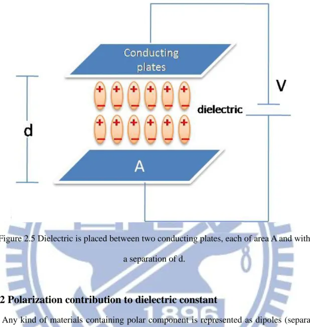
Figure 2.5 Dielectric is placed between two conducting plates, each of area A and with a separation of d. ... 9
Figure 2.6 Variation of dielectric constant with frequency of an alternating electric field. Electronic, ionic, and orientation polarization contribution to the dielectric constant are indicated. ... 10 Figure 2.7 Basic structure of FSG matrix. ... 13 Figure 2.8 Depiction of possible bond rearrangements upon SiOF film hydration to produce Si-OH bonding and the release of HF from the film. ... 13 Figure 2.9 Basic structure units of SSQ dielectric materials consist of random, ladder and cage structures. R= H, CH3 for HSQ and MSQ respectively. ... 14 Figure 2.10 Organic SiLKTM chemical structure units ... 16 Figure 2.11 Relationship of porogen and matrix curing characteristics: (a) viscoelastic behavior of neat organosilicate resin; (b) neat porogen decomposition thermogram; (c) hybrid organosilicate/porogen thermogram. [12] ... 18 Figure 2.12 The conventional formation of porous low-k by using template-type porogen method. ... 19 Figure 2.13 The chemical structure of imidazolium-based ionic liquid ... 22 Figure 2.14 TEM image of calcined ionic liquid template mesoporous silica ... 22
X
Figure 2.15 the mechanism of the self assembly of ionic liquid in silica matrix during solvent
evaporation. ... 23
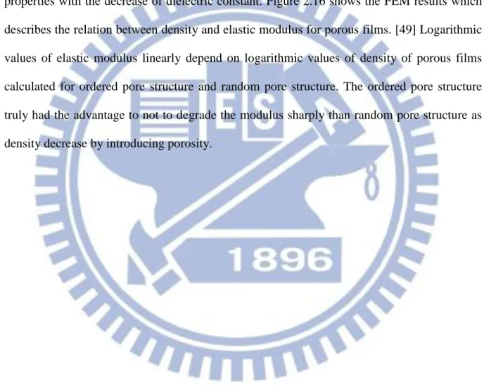
Figure 2.16 Logarithmic plots .of relative elastic modulus and relative density for porous films calculated by FEM. ... 23
Figure 3.1 Process flow for the molecularly template silica films. ... 29
Figure 3.2 Typical curve of n&k measurement ... 32
Figure 3.3 Definition of the angle of incidence and reflection in an XRR experiment... 33
Figure 3.4 Typical geometry of GISAXS measurement. ... 36
Figure 3.5 Schematic diagram of a TEM system. ... 36
Figure 4.1 Relationship of porogen C16mimI and silica curing characteristics. ... 38
Figure 4.2 Isothermal plot of porogen C16mimI decomposition. ... 38
Figure 4.3 Transmission FT-IR spectra of 20% C16mimI template low-k films cured at various temperatures in the 4500-450cm-1 range. ... 40
Figure 4.4 Transmission IR spectra of C16mimI templated low-k films curing at 400℃ with various loading from 5%~30%. ... 41
Figure 4.5 X-ray reflectivity patterns of nonporous silica film and porous silica film. ... 43
Figure 4.6 2D GISAXS scattering pattern of various loading C16mimI templated porous film(C1, C2, C3, C4) after 400℃ calcinations. ... 47
Figure 4.7 Intensity vs. Qy plot to determine the pore spacing in horizontal direction. ... 48
Figure 4.8 Intensity vs. Qz plot to determine the pore spacing in vertical direction. ... 48
Figure 4.9 the ideal model picture depicting the 2D hexagonal pore structure of C4 sample. 51 Figure 4.10 the illustration of micelle formed from C16mimI molecule. ... 52
Figure 4.11 Cross-sectional SEM picture of 20% C16mimI templated porous film (C3) after calcination at 400℃. ... 53
Figure 4.12 Cross-sectional SEM picture of dense silica film after curing at 400℃. ... 54 Figure 4.13 Cross-sectional TEM picture of 20% C16mimI templated porous film (C3) after
XI
calcination at 400℃ at 20,0000x. ... 55 Figure 4.14 Cross-sectional TEM picture of 20% C16mimI templated porous film (C3) after
calcination at 400℃at 40,0000x ... 56 Figure 4.15 The pore structure picture of two type porogen templatd film: (A)PS-P2VP, (B)TEPSS ... 58 Figure 4.16 The chemical structure and micelle structure of C16mimI. ... 58
Figure 4.17 GISAXS scattering pattern of C1 and C2 C16mimI templated film at curing
temperature of RT, 250oC and 400oC. ... 61 Figure 4.18 GISAXS scattering pattern of C3 and C4 C16mimI templated film at curing
temperature of RT, 250oC and 400oC. ... 62 Figure 4.19 The pore spacing changes in z (vertical) and y (horizontal) of C1 film at various curing temperature. ... 63 Figure 4.20 The pore spacing changes in z (vertical) and y (horizontal) of C2 film at various curing temperature. ... 63 Figuer 4.21 The pore spacing changes in z (vertical) and y (horizontal) of C3 film at various curing temperature. ... 64 Figuer 4.22 The pore spacing changes in z (vertical) and y (horizontal) of C4 film at various curing temperature. ... 64 Figure 4.23 Illustration of thickness change during curing process. Pores (blue circle) ... 65
1
Chapter 1 Introduction
1.1 Background
With the downscaling of feature size in integrated circuit, several difficult challenges in the back-end-of-the-line (BEOL) have emerged such as RC (Resistance-Capacitance) delay, crosstalk noise, and power dissipation. [1] Some technology options to mitigate interconnect crisis are circuit design using repeaters, X-architecture, or 3D interconnect and materials design using alternative metal and dielectrics to overcome RC delay. [2] Presently, the utilization of copper (Cu) substituted for Aluminum (Al) as a metal conductor using a dual damascene architecture is the mainstream to reduce resistance. In addition, capacitance is reduced between the interconnect conductor lines by using low dielectric constant materials as an insulator. The original insulator is silicon dioxide (SiO2) with κ= 4.2-3.9. When device
dimension is reduced below 250nm, SiO2 insulator is no longer suitable. Therefore, the need
of lowering the κ-value of bulk SiO2 can be attained by lowering the density of matrix and/or
addition of lower polarizability atoms or bonds. As a result of fervent R&D of low-k material in the past decade, the development of low-κ material yielded fruitful progresses.
For ultra-low- k materials (k<2.5) for 65nm or 45nm node and beyond, since the dense low-κ dielectric has reached its lower limit, [3] there has been much interests in incorporating air (k=1) into dielectric materials as nanopores to produce nanoporous materials with low-k value. [4] Most of ultra-low-k films were made by introducing templating agent [5] into silica structure using spin-on solution coating or plasma-enhanced chemical vapor deposition (PE-CVD). The templating agent or pore generator (porogen) was then removed during the deposition or subsequent thermal process. However, due to large pore size/distribution or interconnected pores caused by porogen aggregation, [6, 7] the template-type porous low-k films faced some critical issues such as (1) low mechanical strength leading to delamination
2
or cracks after chemical-mechanical polish (CMP) and (2) poor barrier/dielectric reliability due to non-continuous side-wall coverage of barrier. Due to the reliability issue, recent efforts focus on creating smaller pores for better mechanical properties with the decrease of dielectric constant by introducing porosity.
Since the meso-, micro- and nanoporous materials have recently attracted much interest due to their promising applications in many areas, researchers utilize these materials as porous low-k candidates. In order to meet the requirement of building meso to micropore well-distributed structure, several porogen candidates have its potential such as ABC (amphiphilic block copolymer) [8] by self-assembly and reactive porogen by grafting method. [9] However, the goal for achieving smaller pores into nanoporous size (<5nm) needs further efforts. Thus, we seek for another porogen candidate with smaller molecular size combining the self-assembly properties and good thermal properties required for integrating into low-k matrix.
Ionic liquid (IL) which possesses the good miscibility to the sol-gel solution and high thermal stability, has now been used in making mesoporous to microporous silica. [10] Utilizing the advantage for low-k application, we designed a long-chain ionic liquid (C16mimI)
to accommodate into porogen route with its self-assembly nature in the proper solvent system. Though have been prepared into mesoporous to microporous silica by previous researchers, ionic liquid is not yet made into application for thin film preparation. The goal now is to make a nanoporous low-k thin film with pore size <5nm and uniformly distributed pore structure. Also, the characterization methodology needs to be established with a systematic discussion about the pore structure information and we want to investigate the porogen behavior in templating into silica matrix.
1.2 Overview
3
reviews the concepts and needs of low-k materials, also accommodate our study motivation and outlook. Chapter 3 presents the experimental methods and instrumentation. Chapter 4 studies the thermal property, porosity, chemical structure and bonding, pore structure and morphology and brief discussion about the ordering of pore structure. Chapter 5 summarizes key results in this study.
4
Chapter 2 Literature Review
2.1 Device scaling and interconnect requirement
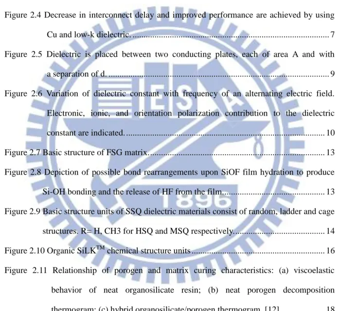
Since the invention of microprocessors, the number of active devices on a chip has been exponentially increasing, approximately doubling every two years. This trend also predicted that the device dimension continuously shrunk towards smaller size according to Moore’s law. Over 50 years, these advances were well-known as scaling, which allowed more active devices to be incorporated in a given area and improved the device characteristics. Figure 2.1 shows the trend of various lengths scaling in the front end of the line. [11] Since the device densities increased, back end (BEOL) interconnect wiring was also forced to shrink to accommodate the increase device densities, as depicted in Figure 2.2.
5
Figure 2.2 Cross-sectional 3D image of a 90 nm IBM microprocessor.
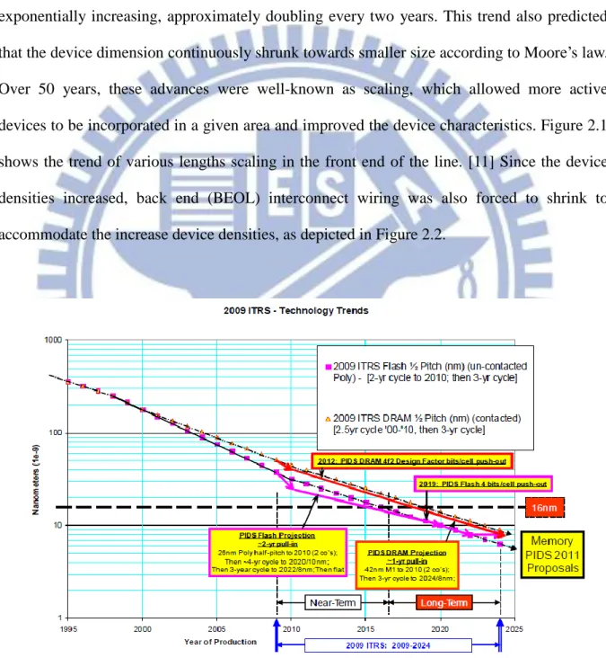
The BEOL signal delay due to continuous feature size shrinking has brought much attention over the decades. It is the product of the back-end resistance and capacitance, RC. In addition, the power consumption and crosstalk problems also result from the capacitance increase. Since one of the major signal delays is associated with interconnect delay, RC delay have become our main concern. Generally, RC delay can be described according to Figure 2.3. By assuming the minimum metal pitch is twice the metal width (W) and the dielectric thickness between the metal lines is the same as the metal height (T), the following equation can be used to predict and calculate the RC delay respectively. [12]
2 0 22 22 m m m t L W L RC (2.1)
where R is the resistivity, Lm is the interconnect line length, W is the interconnect line width, ε
6
higher packing density will lead to the size reduction of W and tm, that will induce higher RC
delay. Therefore, according to above RC delay approximation equation, proper improvement of RC delay can be achieved by modification of resistivity (ρ) of metal line and relative dielectric constant (ε) of inter dielectric layer (ILD).
Figure 2.3 Typical schematic interconnect cross-section with parasitic capacitance
In the early dawn of integrated circuit era, the combination of aluminum (Al) alloys with = 2.7 μΩ.cm and silicon dioxide (SiO2) dielectric has been utilized extensively on the
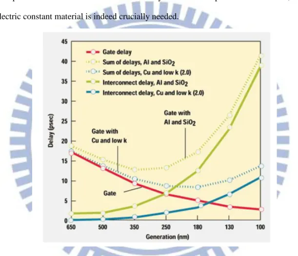
interconnect on account of theirs convenient mature subtractive dry-etch processes and the production compatibility with fabricated device which have no performance issues. Even so, the relentlessly ICs marched down toward smaller geometry size in the pursuit of higher integration density and higher speed has even more demanded on material selection integration. Al/SiO2 interconnect system was no longer eligible to fulfill the device geometry
shrinkage requirement as shown in Figure 2.4. [13, 14] To overcome above mentioned problems, new essential material with low resistivity and low dielectric constant (low-k) for apply as metal line and ILD materials are urgently needed and intensively investigated.
7
Copper (Cu) interconnect are pronounced as one of the most prominent metallization. Possess low resistivity of = 1.8 μΩ.cm, Cu-interconnect is widely developed. Lower interconnect delay is gained from Cu/low-k interconnect system compared to Al/SiO2 interconnect system,
utilizing copper's 37% lower resistivity than aluminum. [15] However, when technology node has run down to 250nm, the limiting factor of Cu-implementation became obviously observe. The capacitance of interconnect is dominated by line-to-line capacitance. Therefore, a lower dielectric constant material is indeed crucially needed.
Figure 2.4 Decrease in interconnect delay and improved performance are achieved by using Cu and low-k dielectric.
When the materials solutions were needed, the options to mitigate interconnect crisis was aimed to new materials to reduce the dielectric permittivity. It is also one of the key “Five difficult challenges through 2009” for the semiconductor industry. Therefore, low-κ material integration is closely related with the optimization between several tradeoffs, especially
8
material properties, device architectures, and process flows. The principle driving forces for future challenge in integrated low-κ material are lower dielectric constant, minimum process cost and higher process reliability/robustness. The ultimatum for any particular technology node will be resolved by the best compromise among these 3 factors. [16]
2.2Definition of low-k dielectric material
2.2.1 Definition of dielectric constant
Dielectric constant (κ) (also called relative permittivity (εr)) is defined as the ratio of the permittivity of substance (ε) to that of vacuum (ε0). When an alternating electric field is
applied through two plates of capacitor/conducting plate with a medium other than vacuum (Figure 2.5), ex. dielectric substance, the dielectric constant will therefore increase. Generally, capacitance(C) is defined as the ratio of charge ±Q on each conductor to the voltage V between them. Conductor plates area (A), by assuming the distance between those two capacitor plates is d, Thus, finalize the capacitance relationship with dielectric constant can be revealed as d A d A V Q C
0 (2.2)in which ε0 is the permittivity of vacuum (ε0=8.845.10-12F/m). Consequently, the capacitance
9
Figure 2.5 Dielectric is placed between two conducting plates, each of area A and with a separation of d.
2.2.2 Polarization contribution to dielectric constant
Any kind of materials containing polar component is represented as dipoles (separation of positive and negative charge in the present of electric field). Dipoles can be characterized by their dipole moment. Many molecules (polar chemical bond) have such dipole moment. From Figure 2.6 which shows the dipoles formation is build up from electronic polarization, ionic polarization and orientation polarization. [17] Electronic polarization is due to the separation of positive charges from negative charges in atoms or molecules of dielectric material due to applied electric field. Ionic polarization occurs in ionic solids whose the dipole moment is disrupted by the application of electric field. Orientation polarization happens in polar dielectric material, which posses permanent electric dipoles. The relationship between polarizability and dielectric constant can be approximately explained by Clausius –Mossotti
10 equation (eq. 2.5) [18] below
e e i i dip dip
r rN
N
N
03
1
2
1
(2.5)where is the relative permittivity or dielectric constant, is the electronic polarization, is the number of atoms/ions per unit volume exhibiting electronic polarization, is the effective ionic polarizability per ion pair and is the number of ion pair per unit volume.
is the number of permanent electric dipole, and is the dipole orientation
polarization.
Figure 2.6 Variation of dielectric constant with frequency of an alternating electric field. Electronic, ionic, and orientation polarization contribution to the dielectric constant are
indicated.
2.2.3 Chemical compound and density reduction
11
2.1. [19] The minimum of polarizability is achieved by single C-C bond. Thereby C-C aliphatic hydrocarbon is being the one of the great potential for low dielectric. Low dielectric might also be obtained by element with small configurational such as smaller atomic radii ex: C-F, C-O and C-H bonds. Conversely, bonding such as C=C double bond or triple bond, need to be avoid, since those bonds have larger polarization due to its increase mobility in π electrons. Although bond enthalpy reveals higher value for double bond and triple bond, which will be an advantages to the higher bond strength compare to single bond. Thus, trade-off stays between lower polarizability that has weaker bond strength while higher bond enthalpy which has higher polarizability.
Table 2.1 Polarizability and bond enthalpy of some chemical bonds
Instead of bonding polarity influence on reduction of dielectric constant, the density of low-k film also one of the dramatic concern. To lower the density can be achieved through increasing the free volume by rearranging the material main structure or introducing porosity. In terms of porosity itself, can be divided into constitutive or subtractive. Constitutive porosity indicates to the self organization of the material, the porous structure is formed without any additional treatment. Pore size less than 2nm usually observed for constitutive
12
porosity and the porosity is relatively low (<15%). Subtractive porosity involves the addition of thermally degradable substance called porogen. Porogen means pore generator which can induce pores in the material after subsequently removal by an annealing process. Pore size ranging from 2nm to tens of nanometers observes for subtractive porosity and the porosity can reach as high as 90%. [20] As a conclusion, organic polymer can combine three approaches. Those include low polarizability bonding, constitutive porosity (introduction of free volume) and the use of porogen by subtractive porosity.
2.3 Classification of low-k dielectric materials
2.4.1 Deposition Method of low-k dielectric materials
Generally, the major deposition techniques for formation of ILD are divided into primary chemical vapor deposition (CVD) known as “dry” process which has been widely adopted by chip manufacturers and showed highly reliable. The second one knows as “wet” process called spin-on method which has not been greatly developed in the process. There are some trade-off between CVD method and spin-on method. Spin-on process simply involves the coating of liquid/viscous precursor on the substrate before final curing to remove the solvent. It provides planarizing property that shows in a smoother surface which is highly desirable. CVD method which involves various gases flow and deposition on the substrate, benefits on cleanliness and minimal waste production. CVD method also provides better conformal coverage of the topography.
2.4.2 Historical trend for low-k dielectric materials
2.4.2.1 Fluorinated Silicates Glasses (FSG)
The first generation of low-k material were fluorinated silicate glasses (FSG) invented by Novellus System Inc. FSG has dielectric constant value as low as k=3.6. FSG posses lower dielectric constant than SiO2 due to incorporation of fluorine into SiO2 matrix film. Fluorine
13
incorporation leads to a less dense, more porous film by creating voids in the SiO2 matrix.
Typical FSG film matrix shows in Figure 2.7. Replacing Si–O in the SiO2 matrix with Si–F
reduces the polarizability of the matrix. The above reasons contribute to a lower dielectric constant of the FSG dielectric layer. [21, 22] FSG film has some drawback, for instance SiOF film is hydrophobic, in the meantime the fluorine atom will tend to react with hydrogen atom from water absorb in the release of HF moisture when heated to elevate temperature. The moisture of HF will travel along the interface of ILD and metal causing adhesion become poorer as explained by Figure 2.8. [23]
Figure 2.7 Basic structure of FSG matrix.
Figure 2.8 Depiction of possible bond rearrangements upon SiOF film hydration to produce Si-OH bonding and the release of HF from the film.
14 2.4.2.2 Silsesquioxane (SSQ) based
Silsesquioxane (SSQ) based low-k material or commonly called T-resin are organic-inorganic polymer with empirical chemical formula RSiO1.5. The substituents (R) can
include hydrogen, alkyl, alkenyl, alkoxy and aryl. The contribution of these organic substituents benefit in lowering the dielectric constant because they provide lower density of the matrix structure. For the addition, they also attributed to less polarizability organic bond (Si-CH3) compare with Si-O bonds in SiO2. SSQ based low-k also known as organosilica
glasses (OSG) which yield k=2.7-3.0. The common used SSQ based materials for microelectronic application are mainly hydrogen-silsesquioxane (HSQ) and methyl-silsesquioxane (MSQ). HSQ has hydrogen as a terminal group and MSQ has methyl as a terminal group. The structure of basic units of SSQ shows in Figure 2.9. [24]
Figure 2.9 Basic structure units of SSQ dielectric materials consist of random, ladder and cage structures. R= H, CH3 for HSQ and MSQ respectively.
15
MSQ material has lower dielectric constant compare to HSQ. The contribution of larger –CH3 group that will cause steric hindrance rather than smaller –H group will lower the
density of MSQ matrix. The Si-CH3 bond is also a less polarizable bond compare to Si-H.
Thus greatly reduce the dielectric constant of MSQ. Table 2.3 summarizes the principle properties of SSQ based dielectric materials compare with SiO2. Subsequently, the
commercially available SSQ based low-k materials are summarized in Table 2.4 which has k < 3.0. [25, 26]
Table 2.2 Principle properties of SSQ based dielectric materials
Property MSQ HSQ SiO2
Dielectric Constant 2.8 3.0 4.0
E Modulus (GPa) 3-5 6 59
Density (g/cm3) 1.2-1.3 1.4-1.5 2.4
Tensile Strength (MPa) 50 80 -
Table 2.3 Commercially available SSQ-based low-k materials
Material Trade Name k-value Company
HSQ Fox (flowable oxide) 2.9-3.0 Dow Corning
MSQ RZ25-15 2.6 Hitachi
MSQ HOSP 2.6 Honeywell
Porous HSQ XLK 2.2 Dow Corning
Porous HSQ LKD 5109 2.2-2.3 JSR
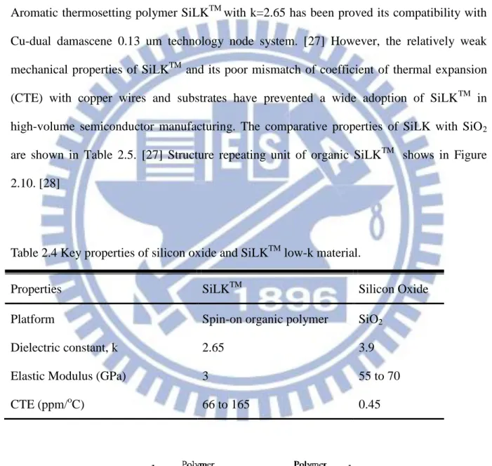
16 2.4.2.4 SiLKTM
Spin-coated base SiLKTM was an organic polymer dielectric founded by Dow Chemical in mid 1997. In April 2000, IBM reported the complete integration of SiLKTM dielectric and copper wiring, and announced its intent to commercially fabricate integrated circuits using SiLKTM resin. Toshiba/Sony and Fujitsu also accommodated SiLK resin with hybrid stacks. Aromatic thermosetting polymer SiLKTM with k=2.65 has been proved its compatibility with Cu-dual damascene 0.13 um technology node system. [27] However, the relatively weak mechanical properties of SiLKTM and its poor mismatch of coefficient of thermal expansion (CTE) with copper wires and substrates have prevented a wide adoption of SiLKTM in high-volume semiconductor manufacturing. The comparative properties of SiLK with SiO2
are shown in Table 2.5. [27] Structure repeating unit of organic SiLKTM shows in Figure 2.10. [28]
Table 2.4 Key properties of silicon oxide and SiLKTM low-k material.
Properties SiLKTM Silicon Oxide
Platform Spin-on organic polymer SiO2
Dielectric constant, k 2.65 3.9
Elastic Modulus (GPa) 3 55 to 70
CTE (ppm/oC) 66 to 165 0.45
17 2.4.2.5 Porous low-k materials
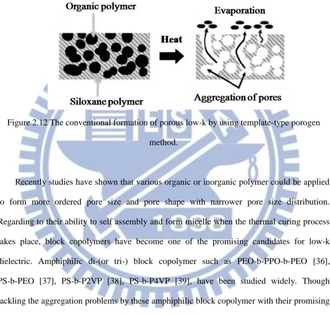
The above mentioned low-k materials were all classified into dense low-k materials. In order to reach k<2.5, fully densified materials has seemingly reached their lowest capability. Hence, the research has to move on with introduction of porosity onto the dense materials. That is, to incorporate air (k = 1) to the matrix. While porogen can be used in spin-on organosilicates to obtain k = 2.4 and lower, the decision was initially made to design porogen-free spin-on systems because of their simplicity, lower cost. The examples of porogen-free systems are aerogel and xerogel low-k film. [29] While low dielectric constants can be obtained in the case of aerogels or xerogels, control of the pore size is difficult to achieve and the processing conditions are not always compatible with mainstream manufacturing. [30]
Another strategy of making porous low-k film is to accommodate the sacrificial materials which are also called “porogen” or pore generator that are decomposed upon the thermal process. This approach which is sometimes referred to as a subtractive pore-generation route uses a low-molecular-weight thermosetting polymer dissolved in a suitable organic solvent, together with a second component with appropriate thermal properties to act as a porogen. Porogens can vary greatly, and examples ranging from small molecules, such as cyclodextrins (CDs), to surfactant, linear and branched polymers, and cross-linked particles have been examined. Such formulations are spin-coated onto a substrate and generally hot-baked to remove both the majority of spinning solvent. This coating is then heated directly to temperatures of above ~400℃. The high temperatures complete the curing of the matrix and decompose the porogen into small fragments, which can diffuse through the matrix and leave behind pores. From the review article of low-dielectric constant materials, [12] a number of prerequisites have to be met. First, the porogen and matrix precursor have to be either soluble or compatible in the form of a colloidal dispersion to yield optically transparent solutions. Second, the components must be
18
mutually compatible to produce uniform films after spinning and optically transparent films after solvent evaporation. Finally, the thermosetting matrix has to stiffen sufficiently during the high-temperature cure prior to porogen decomposition to resist the capillary forces acting to collapse the pores during porogen decomposition. Figure 2.11 illustrates the thermal behavior of the various components in an ideal system. As a result, the candidate of porogen for good thermal stability would be limited to the polymer material whose thermal property could be well tuned by various molecular weights or functional group.
Figure 2.11 Relationship of porogen and matrix curing characteristics: (a) viscoelastic behavior of neat organosilicate resin; (b) neat porogen decomposition thermogram; (c) hybrid
organosilicate/porogen thermogram. [12]
However, during thermal heating process, the random distribution of pores created by porogen removal tends to agglomerate and coalescence which cause a burden to the mechanical strength of final SiO2 film especially when the porogen loading is increased as
shown in Figure 2.12. [31, 32] In solving the problem of large pore due to aggregation of the porogen, another method uses chemically linked or grafted to the SiO2 polymer. [33, 34, 35]
19
This method can achieve better control of porogen distribution in the SiO2 dielectric film.
Porogen selection must be compatible with SiO2 matrix precursor in order to avoid phase
separation.
Figure 2.12 The conventional formation of porous low-k by using template-type porogen method.
Recently studies have shown that various organic or inorganic polymer could be applied to form more ordered pore size and pore shape with narrower pore size distribution. Regarding to their ability to self assembly and form micelle when the thermal curing process takes place, block copolymers have become one of the promising candidates for low-k dielectric. Amphiphilic di-(or tri-) block copolymer such as PEO-b-PPO-b-PEO [36], PS-b-PEO [37], PS-b-P2VP [38], PS-b-P4VP [39], have been studied widely. Though tackling the aggregation problems by these amphiphilic block copolymer with their promising properties in making the mesoporous low-k film with pore size below ~10 nm, it’s not enough when the requirement of smaller pore size is thought to be suited the future challenge.
2.4.2.6 Ionic liquid templated mesoporous silica
Recently ionic liquids (IL) have attracted considerable interest not only in chemistry, but also in materials science. [40] ILs have been utilized as clean solvents and catalysts for green
20
chemistry and as electrolytes for batteries, photochemistry, and electrosynthesis, [41, 42] but their potential as templates for nanostructured materials is less commonly known. ILs derived from 1-alyl-3-methylimidazolium are of particular interest because, by changing the alkyl chain length or the anion, a wide variation of properties such as hydrophobicity, viscosity, density and solvation strength can be obtained. Figure 2.13 shows the chemical structure of ionic liquid commonly used in chemistry. [43] The character of an ionic liquid can be tuned comparatively easily by the choice of the cation/anion combination. Physical and chemical properties that are dependent on the cation/anion combination include miscibility of the IL with water, organic solvents, dissolution of gases, basicity, coordination power, viscosity, thermal stability and many further properties. In the application of mesoporous materials, the ionic liquid has been used as the structure directing agent for preparing porous silica with order structure. Figure 2.14 showed the TEM picture of the mesoporous silica of the powder sample templated by the ionic liquid in the literature. [44] The pore size of mesoporous or near microporous can be successfully made by templating the long-chain ionic liquid into silica matrix with its amiphiphilic self-assembly property.
Compared to the amphiphilic bolok copolymer, ionic liquid possess small pore size and establishes a narrower size distribution due to its low molecular weight. [45] Higher porogen loading can be introduced without further porogen aggregation upon heating. Also, due to the versatile properties such as amphiphilicity or thermal stability which is tunable by easily changing its chemical structure in either alkyl chain length [46] or anion species. [47] Due to the versatile structure and property, ionic liquid has the potential to be applied to the low-k process due to its amphiphilicity and thermal stability. When the ionic liquid is put into a certain solvent system (e.g. Ethanol) with silica precursor (e.g. TEOS), it may self assemble to a micelle and due to its charge surface of the nature, leading to the electrorepulsive aggregates. So far, the porous silica film structure using ionic liquid as template has not been studied. We proposed the probable mechanism of the silica/ionic liquid thin film system shown in the
21
Figure 2.15. The mechanism called “Evaporation induced self-assembly” proposed by J. Brinker et al. studying the film system to prepare a mesoporous thin film was accomplished by block copolymer or the ionic surfactant. [48] Thus, the templating behavior of ionic liquid into low-k thin film has come into an interesting part. As a new materials applied to low-k dielectrics, we hoped that ionic liquid templated silica thin film may possess a more regular structure than randomly distributed porogen due to the better properties such as mechanical properties with the decrease of dielectric constant. Figure 2.16 shows the FEM results which describes the relation between density and elastic modulus for porous films. [49] Logarithmic values of elastic modulus linearly depend on logarithmic values of density of porous films calculated for ordered pore structure and random pore structure. The ordered pore structure truly had the advantage to not to degrade the modulus sharply than random pore structure as density decrease by introducing porosity.
22
Figure 2.13 The chemical structure of imidazolium-based ionic liquid
23
Figure 2.15 the mechanism of the self assembly of ionic liquid in silica matrix during solvent evaporation.
Figure 2.16 Logarithmic plots .of relative elastic modulus and relative density for porous films calculated by FEM.
24
Chapter 3 Experimental Section
This chapter described the experimental methods and steps, including all the chemicals used in the solution, precursor solution preparation, film preparation, and all the characterization methodology.
3.1 Preparation of low-k films
3.1.1 Chemicals
(1) Tetraethoxysilane
TEOS, CAS No.78-10-4, KBE-04 product by Shin-Etsu Chemical Co.
(2) Hydrochloric acid
HCl, CAS No.7647-01-0, product by Sigma-Aldrich Co.
(3) 1-iodohexadecane
CH3(CH2)14CH2I, CAS No.544-77-4, contains copper as stabilizer, 95%, product by
25 (4) 1-methyl imidazole
CAS No.616-47-7 >99.0% product by Sigma-Aldrich Co.
(5) 1-Hexadecyl-3-methylimidazolium iodide [C16mim][I], synthesized in lab
(6) Ethanol
26 (7) Tetrahydrofuran
THF CAS No.109-99-9, >99.9%, prduct by ECHO Co.
(8) Toluene
27
3.1.2 Preparation of low-k precursor solution
3.1.2.1 Preparation of [C16mim][I]
The Ionic liquid [C16mim][I] was synthesized according to a reported route. [50] As a
typical synthesis, an excess of 1-hexadecyliodide was mixed with 1-methylimidazole. The mixture was put into 250mL flask, refluxed at 90℃ for 48 hours, and then cooled to room temperature. The product was further washed by toluene and THF co-solvent. After being washed several times, the impurity can be removed by co-solvent and the crystalline [C16mim][I] white powder was collected by vacuum filtration and dried in air at room
temperature.
3.1.2.2 Preparation of low-k precursor solution
Precursor solutions were prepared by addition of porogen([C16mim][I]) to polymeric sols
made in acidic conditions. In a typical sol preparation, TEOS (Si(OC2H5)4), water (pH=1.25
with HCl) and ethanol(mole ratio= 1 : 5 : 3.8) were mixed. After magnetic stirring at 25℃, the sols were aged at 60℃ for 12 hours. The porogen([C16mim][I]) was then ultrasonically mixed
into the sol, which can be eventually diluted with ethanol. The various weight percent of porogen was chosen and the final ratio of all the content of the sol was shown in Table 3.1 below. The various porogen loading of solution were designated as C1 through C4 and summarized in table 3.2.
Table 3.1 The composition of the low-k sol prior to spin coating
Low-k solutions components
TEOS H2O EtOH Porogen
([C16mim][I])
HCl
28 Table 3.2 The composition of various
Low-k solutions components C1 C2 C3 C4 Porogen/SiO2+porogen composite (wt%) 5% 10% 20% 30%
3.1.3 Deposition and thermal treatment of low-k thin film
Before spin coating, the precursor solution was initially filtered through a 0.2 µm PTFE filter in another bottle, and then placed in anultrasonic bath for 1 minute to ensure no bubble in the solution. The precursor was spin coating onto silicon wafer. Prior to deposition, the silicon wafer were cleaned in detergent, distilled water and ethanol for 15 min, respectively, followed by drying in a flow of nitrogen. The angular velocity range of the spinner was 2000 rpm and the spin time was 40 seconds. After deposition the sample plates were dried in air at room temperature for 24 hours. Calcined films were obtained by heating in air at 400℃ for 12 hours, which ensures complete removal of organic species. Figure 3.1 presented the process flow of preparation of molecularly template silica films.
29
30
3.2 Characterization techniques and methodologies
The thickness and the refractive index of low-k thin films were analyzed by using n&k Analyzer which was an optically non-destructive measurement tool. In order to understand the chemical bondings in low-k thin films, Fourier transform infrared spectroscopy (FT-IR) was used to verify the chemical makeup and structural information of Si-O-Si of the thin films and also, the signals change due to porogen removal. As well as chemical bonding evidence, molecular structure verification would lead to the early stage of explanation about chemical system identification.
X-ray reflectivity (XRR) was utilized to characterize the density of low-k films. Porosity was also calculated based on density data. Moreover, the pore geometry parameters such as pore size, pore size distribution, pore to pore distance were characterized by using grazing incidence small angle X-ray scattering (GISAXS) tools. GISAXS was a prominent tool that could absolutely give the entire information about these parameters effectively. We also can get the pore information and the surface morphology of the porous thin films by using scanning electron microscopy (SEM) and transmission electron microscopy (TEM).
One of the main properties of low-k film was dielectric constant value (κ). This electrical property was measured by employed MIS (metal-insulator-semiconductor) structure method.
The following part of this chapter was the characterization methodologies and principle involved in this research. We used these techniques to clarify the structure and properties of all the prepared low-k thin films.
3.2.1 Thermal Gravimetric Analysis (TGA)
The testing of thermo-gravimetric analysis (TGA, TA Q-500) was performed on the samples to determine changes in the weight of sample in relation of the change in temperature.
31
The analysis testing depended on high degree of precision in three measurements: weight, temperature and temperature change. The TGA testing was usually used in research and testing to determine degradation temperatures, organic and inorganic constituent in materials, and solvent residues.
3.2.2 Fourier Transform Infrared Spectroscopy (FT-IR)
FTIR has been extensively applied to qualitative analysis of organic compounds due to the specific absorption wavelength by different vibration and rotation modes in the infrared wavelength range. In our case, the inorganic-organic composite thin film can also be identified by associating the frequency of the vibrations with a particular bond type such as Si-O-Si bonding type. A Perkir Elmer Spectrum 100 FT-IR was employed in our analysis. Also, transmission mode of low-k films/silicon wafer sample was chosen to characterize the chemical makeup and structural information. The S/N ratio was very small for thin film measurement using transmission mode. IR data was collected in the wavenumber ranging from 4000 to 400 cm-1 using a total of 32 scans at 4 cm-1 resolution.
3.2.3 n&k analyzer
The optical dielectric constant can be calculated by the value of refractive index(ε =n2). The n&k analyzer 1200 was used in this study to obtain refractive index (n) and film thickness (d) information of low-k films. The experimental steps were listed below:
1. To scan standard sample as a baseline. (The wavelength ranged from 190 nm to 900 nm.) 2. To put sample wafer upside down on the n&k analyzer, and then scan again to collect the
typical experimental curve illustrated in Figure 3.2.
The experimental curve was fitted using Forouhi-Boomer Dispersion relation [51](Equation 3.1) to deduce refractive index (n) and film thickness (d).
32
q i i i i i C E B E C E B n E n 1 2 0 0 ) ( ) ( (3.1) where B E B E C Q A B g g2 2 0 2
E C B E C Q A C g 2 g 2 2 0
2 1 2 4 2 1 B C Q E:Incident energy of light
B, C:Parameter which relate to electron structure of materials Q:Number of terms
n (∞) > 1
Figure 3.2 Typical curve of n&k measurement
3.2.4 X-ray Reflectivity (XRR)
33
Advance X-ray Diffractometer with Cu Kα source (λ=0.154nm) using θ-2θ or also called ω-2θ. X-ray reflectivity (XRR) was conveniently applied for the structural studies of both crystalline and amorphous multilayer samples. XRR was an adequate tool to analyze density, thickness, and roughness of thin films. When the incident angle is very small (grazing incident angle ω), the entire incident beam can be reflected and its intensity would decrease with increase of incident angle. The reflected angle 2θ was recorded as shown in Figure 3.3. This type of scanning also called ω-2θ scan. The initial ω angle was set to 0.3°. The θ scanning region started from 0° to 2°.
Figure 3.3 Definition of the angle of incidence and reflection in an XRR experiment
The reflection at surface and interfaces was as a result of the distinct electron densities from different layers or films. Due to its different reflective index from different layers, it would emerge different reflection intensity. The complex refractive index of x-ray region was slightly less than 1 and could be expressed by equation 3.1 below. [52]
i
n
1
(3.1)34
number; A, atomic mass; and ρ, mass density. δ and β represented the dispersion and absorption respectively. For the frequency greater than resonance frequency, δ could be further expressed by equation 3.2:
e e
n
r
c
m
n
e
.
2
)
2
(
2
2 0 2 2 0 2
(3.2)where r0 was the Bohr atomic radius and ne was the electron density. Electron density ne was
the number of electron per atom (Z) multiplied by number of atom (natom). Z was usually
replaced by complex atom form factor f=f0+f’+if’’= Z+f’+if’’. Furthermore, natom was related
to the density of material (ρ) by equation 3.3:
A
N
n
Aatom
(3.3)With NA and A were the Avogadro number and the atomic weight respectively. For incident
angles below a critical angle, θc, (θ<θc), total reflection occurs. The θc could be finally
reduced to relate with ρ by equation 3.4:
2 ( '). 2 0 A f Z N r A c (3.4)
For incident angles greater than θc, (θ>θc), the x-ray beam penetrated inside the film.
Therefore, reflection occurred at the top and bottom surfaces of the film. Interference between the rays reflected from the top and the bottom of the film surface would generate interference fringes which related to the thickness of film (d) by equation 3.5:
35 m m
d
11
2
for (3.5)3.2.5 Grazing Incidence Small Angle Scattering X-ray (GISAXS)
Grazing-Incidence Small-Angle X-ray Scattering (GISAXS) was a versatile tool for characterizing nanoscale density correlations and/or the shape of nanoscopic objects at surfaces, at buried interfaces, or in thin films. GISAXS combined features from Small-Angle X-ray Scattering (the mesoscopic length scale, incident beam definition by multiple slits, area detector) and diffuse X-ray Reflectivity (the scattering geometry and sample goniometer). In order to make x-ray scattering surface sensitive, a grazing incidence angle αi is chosen
between about half the critical angle
αc and several critical angles of the film material GISAXS measurements were performed at
the BL23A beam-line of the National Synchrotron Radiation Research Center (NSRRC). The incidence beam, extracted from a super-conducting wavelength-shifter (SWLC) X-ray source, was monochromated to a wavelength λ of 0.155nm by a Ge(111) double crystal monochromator, with Δλ/λ~10-3
. The two dimensional image were recorded by a low-noise 16-bit charge-coupled device (CCD) camera. All the GISAXS data were corrected for sample transmission, background, and the detector sensitivity. The typical geometry of GISAXS measurement was depicted in Figure 3.4. The area detector records the scattering intensity of scattered rays over a range of exit angles αf and scattering angles 2θf in the surface plane. [53]
36
Figure 3.4 Typical geometry of GISAXS measurement.
3.2.6 Transmission electron microscopy (TEM)
Transmission electron microscopy (TEM) (JEM-2010F) was used to study the pore morphology of the film. Figure 3.5 showed the schematic diagram of TEM system.
37
Chapter 4 Results and discussion
4.1 The thermal requirement of low-k porous films
The introduction of porosity into spin-on silica was accomplished by a sacrificial pore generator that was removed during the curing of the materials. So, this approach used so called “subtractive pore-generation route” to hybrid the small molecule porogen, C16mimI, to
the silica matrix. In order to get a porous film with good film properties during curing of silica matrix, we concerned the thermal properties of the porogen and so as to the silica/porogen hybrid. At first, the initial silica precursor was gradually polymerized as temperature increased while porogen was well incorporated in the matrix. As temperature increased to a level, the structure could be stiffened at about 200~250℃ as literature said [12]. At the end, the porogen should be removed from the matrix upon higher temperature curing. Therefore, for the requirement that the thermosetting matrix had to stiffen sufficiently prior to porogen decomposition to resist the capillary forces acting to collapse the pores, the Td (decomposition
temperature) should be higher than 250℃.
Figure 4.1 illustrated the thermal behavior of the porogen and silica/porogen hybrid in TGA profile. The 10wt% decomposition temperature of pure porogen C16mimI ,Td10,was
~270℃. Also, the decomposition can be accomplished in a fast way, as shown by the isothermal TGA plot in Figure 4.2. Upon heating in 270℃, the porogen degraded sharply as time went by, and we can see nearly all the content could be removed after ~15min heating. We also can see the similar trend of thermal characteristics in the silica/porogen hybrid that the porogen started to degrade above ~250℃ and finally completed its decomposition at higher temperature. In spite of the small amount of weight loss may be due to dehydration at ~250℃ during curing in the hybrid, this result provided a promising thermal stability to meet the requirement in making a porous low-k film.
38
Figure 4.1 Relationship of porogen C16mimI and silica curing characteristics.
39
4.2 Structure characterization
4.2.1 Chemical bonding of IL-templated mesoporous silica films
The Fourier-transform infrared spectra of IL-templated low-k films were performed in the range from 450 to 4000cm-1. Figure 4.3 presented the FTIR spectra of the prepared films obtained at various calcinations temperatures for removing the ionic liquid C16mimI, which
showed several different features attributed to silica, the templating ionic liquid and residual water. In the temperature region below 250℃, The presence of ionic liquid C16mimI was
characterized by two intense absorption bands (2853, 2923cm-1) assigned to CH2 stretching
vibrations. Other two weak bands due to imidazole ring structure of C16mimI were found in 1468 and 1165cm-1. The two main peaks characteristic of Si-O-Si bonds vibration modes were detected around 1070 and 800cm-1. The lower frequency mode around 800cm-1 was assigned to Si-O-Si symmetric stretching; while the higher frequency mode around 1075cm-1, which intensity was the larger one, was assigned to antisymmetric stretching (TO3 mode). [54] The
TO3 band appeared generally accompanied by a shoulder at the higher frequency side around
~1200cm-1. A band of medium intensity centered near 960cm-1 was attributed to Si-OH stretching vibrations. This band might overlap with Si-O-, Si-O-C (from unhydrolyzed OEt groups). A broad intense band was detected between 3000 and 3800cm-1, due to O-H vibrations from different species. Two main groups of bands could be found in around 3800-3650cm-1, stretching modes of isolated OH groups or OH groups partially involved in hydrogen bonding and around 3650-3200cm-1, stretching modes of strongly hydrogen-bonded OH groups.
40
Figure 4.3 Transmission FT-IR spectra of 20% C16mimI template low-k films cured at various
temperatures in the 4500-450cm-1 range.
As we can see in Figure 4.3, the spectra showed some changes as temperature increased. First, from characteristic peak of C16mimI, i.e. the peaks in 2923, 2853, 1468, 1165cm-1, all
disappeared at 300℃. We ensured that the result from these peak changes was consistent with the thermal properties shown in TGA. All The porogen could be removed above 270℃, creating pore structure inside the matrix. Second of all, the intensity from O-H peak around 3400cm-1 gradually decreased as temperature increased to 250℃. This phenomenon may be due to the condensation of silanols with elimination of water. While above 300℃, a sudden increase in intensity of the O-H stretching band was observed. Because the porogen was removed out of the silica, the pore may easily absorb water in the surface with unreacted silanol group. In summary, the chemical structure change from C16mimI templated hybrid to
porous film can be checked by IR spectra in certain characteristic peaks.
400℃ 300℃ 250℃ 200℃ 150℃ 100℃ 50℃ As deposited
41
Figure 4.4 Transmission IR spectra of C16mimI templated low-k films curing at 400℃ with various loading from 5%~30%.
4.3 Pore characterization of porous film
This part discussed the pore structure prepared by templating long-chain ionic liquid (C16mimI) to the silica matrix including film density, porosity, pore size, pore to pore spacing
and pore size distribution.
4.3.1 Porosity
In order to clearly know the information about pore structure, the porosity needed to be known well. Figure 4.5 showed the X-ray reflectivity spectra of the dense silica film and the C16mimI template porous silica film. We used X-ray reflectivity to examine the film density
42 2 ( '). 2 0 A f Z N r A c (4.1)
where ρ was the density of porous NCS film. When the scanning proceeded at very low angle, a total reflection occurred. The initial sudden drop corresponded to a penetration of X-ray into film. The angle of first sudden drop was called critical angle (θcrit 1). The second critical angle
(θcrit 2) was the characteristic of the denser silicon substrate. This first critical angle (θcrit 1)
was accurately related to the electron density of the film, which could be related to the bulk density of the film. Therefore, the θcrit 1 was related to the density of nonporous or porous
film. If the density of porous film was precisely known, the film’s porosity could be calculated based on Equation 4.2. [55]
s.
1
(4.2)where ρ was film density (g/cm3), ρs was silica density, and φ referred to porosity. Generally if
the density of porous films increased, the porosity reduced. Table 4.1 showed the density and porosity of dense silica film and porous silica film by using XRR. The porosity of 41.1% can be created by introducing 30wt% porogen to silica precursor. The loading of porogen (C16mimI) increased from C1 to C4, thus porosity increased form C1 to C4
43
Figure 4.5 X-ray reflectivity patterns of nonporous silica film and porous silica film.
Table 4.1 Density and porosity of dense silica film and porous silica film by using XRR
materials Density (g/cm3) Porosity (%)
Dense silica film 1.90 /
C1(5%) 1.80 5.3% C2(10%) 1.65 13.2% C3(20%) 1.23 35.3% C4(30%) 1.12 41.1%
C1
C2
C3
C4
Dense silica
44
4.3.2 Pore morphology by GISAXS
4.3.2.1 GISAXS theorem
From the theorem of GISAXS, it was defined that the intensity of scattering pattern was proportional to the product of intra-particle structure factor (form factor), P(q) and inter-particle structure factor S(q) (structure factor):[56]
)
(
)
(
)
(
)
(
q
n
2V
2P
q
S
q
I
p
p
m p (4.3)where np was the number density of particles, ρp and ρm were the scattering length density
of the particle and the matrix, respectively, Vp denoted the volume of the particle,where q was
the scattering wave vector. The scattering wave vector, q, was defined by:
sin
4
q
(4.4)where θ and λ were the scattering angle and wavelength of radiation employed.
4.3.2.2 Pore morphology analysis by pore spacing and pore size
Figure 4.6 displayed GISAXS scattering patterns for various loading of C16mimI
templated silica films after calcined at 400oC. From C1 to C4 films, the well defined ring of maxima scattering pattern appeared in high-Q region was observed. For C1 to C3 films, no specific scattering dots shown in the pattern means that the organization of pores are isotropic. Though the structure could not be well determined, the distribution of pores were assumed to be partially ordered with no preferred direction according to the halo ring of maxima scattering. However, the C4 film showed more organized structure with some clear dots
45
appeared on the scattering pattern. The GISAXS pattern of C4 film reveals a distorted 2D hexagonal structure with anisotropic distribution of pores. [57]
46 0.05 0.1 Qy(Å -1 ) 0.05 0.1 0.15 0.2 Qz(Å-1) 0.05 0.1 0.15 0.2 Qz(Å -1 ) Qy(Å-1) 0.05 0.1 C1-400oC C2-400oC C3-400oC C4-400oC 0.05 0.1 0.15 Qy(Å-1) 0.05 0.1 0.15 0.2 Qz(Å-1) Qy(Å-1) 0.05 0.1 0.15 0.1 0.05 0.2 0.3 0.25 0.15 Qz(Å-1)