國 立 交 通 大 學
電子工程學系電子研究所
博 士 論 文
銦錫氧化物電極與表面結構改進新穎氮化鎵發光
元件特性之研究
Novel GaN-based Light-emitting Devices with
Indium Tin Oxide Contacts and Surface Structure
Modifications
研 究 生 :朱 俊 宜
指導教授 :張 國 明
銦錫氧化物電極與表面結構改進新穎氮化鎵發光元件特性
之研究
Novel GaN-based Light-emitting Devices with Indium Tin
Oxide Contacts and Surface Structure Modifications
研 究 生:朱俊宜
Student: Jiunn-Yi Chu
指導教授 : 張國明 博士 Advisor: Dr. Kow-Ming Chang
國立交通大學
電子工程學系電子研究所
博士論文
A Dissertation
Submitted to Department of Electronics Engineering & Institute of Electronics College of Electrical and Computer Engineering
National Chiao Tung University In Partial Fulfillment of Requirements For the Degree of Doctor of Philosophy
In
Electronics Engineering January 2007
Hsinchu, Taiwan, Republic of China
銦錫氧化物電極與表面結構改進新穎氮化鎵發光元件
特性之研究
研究生:朱俊宜
指導教授:張國明 博士
國立交通大學
電子工程系電子研究所
摘要
最近氮化鎵發光元件由於其多用途的應用和市場需求的迅速的發展吸引了 眾人的目光,並使得相繼投入研究。自從氮化鎵發光二極體在西元一九九三年問 世以來,高亮度氮化鎵發光二極體已成功地應用在行動電話鍵盤的發光模組、液 晶顯示器背光源、照相機閃光燈和高色彩飽和度的戶外顯示器上。而這些發光元 件更被視為將改變人們的生活模式並且舒緩嚴重的能源危機,不過依照目前元件 的發光效率,氮化鎵發光二極體仍然比不上傳統的光源系統,因此氮化鎵發光二 極體若要應用在固態照明上並且取代傳統的光源系統,許多限制了光輸出轉換效 率的技術,譬如磊晶結構品質、P 型半導體的歐姆電極、出光效率、以及散熱問 題等等必須得到長足的改善。 在這篇論文當中,提出了幾種方法來改進氮化鎵發光元件其出光效率,包含 使用具有較低吸收係數的導電電極來取代原有的金屬電極以及元件表面結構上 的修改。在論文第一部分,採用銦錫氧化物來取代傳統的鎳金電極,並分析其發光元件的特性,銦錫氧化物為一具有高光穿透性的導電物質,不過由於銦錫氧化 物與P型氮化鎵半導體的功函數差異甚大,因此使得銦錫氧化物在P型氮化鎵半導 體上呈現蕭基接點的特性,因此在二者間插入一層薄的P型氮化鎵銦磊晶層,以 降低其蕭基位能障,形成近似甌姆特性的接點。經由 XPS, XRD及 SIMS分析的 結果,其介面形成機制主要是由於鎵原子的擴散並和氧化物的氧原子形成鍵結, 造成鎵原子空缺,使得局部載子濃度的提高,進而提升內建電場強度和載子穿遂 此介面的機率,因而降低此界面接觸電阻,形成近似歐姆接點。在分析此歐姆介 面的主要電流傳導機制時,量測環境溫度對介面接觸電阻係數的影響,發現此介 面電流的主要傳導機制和介面的合金條件相關,在不同的合金溫度處理下,當處 理溫度由 400oC提高成 600oC時,此介面的主要傳導電流機制為熱場發射傳導傾 向為熱離子發射傳導。 雖然銦錫氧化物無法形成較鎳金電極良好之甌姆接點於P型氮化鎵上,但在 相當於元件正常工作條件 27 A-cm-2的電流密度流過銦錫氧化物和P型氮化鎵的 介面時,其接觸電阻係數約2.6 x 10⁻² ohm-cm2 ,雖然仍未盡理想,但是已經足 夠應用在二極體上,而不至於產生過多的串接電阻,進而損耗過多的能量。使用 銦錫氧化物為電極的氮化鎵發光二極體其整體特性表現如下,當20 mA的電流注 入時,順向電壓約為3.43 V,雖然比傳統上使用鎳金金屬電極的發光二極體高了 約0.2 V, 但是外部量子效率和能量轉換效率卻分別提升了 46% 和 36%,這效 率上的提升主要是減少了半透明金屬電極的吸收。 至於壽命試驗,經過 500oC 退火處理的銦錫氧化物氮化鎵發光二極體,表現了類似傳統上使用鎳金金屬層的 氮化鎵發光二極體的可靠度行為。因此,藉由中間層P型氮化鎵銦磊晶層的加入, 使得銦錫氧化物能夠應用在高亮度、高可靠度的氮化鎵發光元件上。 在製作發光元件時,採用平台式的結構,正負電極位於絕緣基板的同一面, 所以元件的操作電流為橫向傳導。然而在這個結構下,橫向傳導電流可能導致正
負電極附近電流過度擁擠,此效應將會影響元件的可靠度。因此,妥善的處理橫 向傳導電流,避免元件在操作時產生局部過熱的現象是不可或免的。由於銦錫氧 化物的導電特性遠不如金屬,所以當應用在氮化鎵發光元件時,必須考慮到透明 電極厚度對元件特性的影響。當20 mA 的電流注入時,60 奈米、180 奈米和 300 奈米厚銦錫氧化物薄膜電極的氮化鎵發光元件的順向電壓分別為 3.45、3.42 及 3.32 V,而輸出光功率則幾乎沒有太大的分別,但是所對應的光輸出轉換效率則 和順向電壓及串接電阻成反向關係。除此之外,從元件操作電流密度分佈的模 擬,60 奈米厚銦錫氧化物薄膜電極氮化鎵發光元件面臨嚴重電流散佈不均的問 題,此問題將會導致電流擁擠效應且產生局部過熱的現象,在實驗中此元件在經 過1008 小時可靠度測試後,光輸出功率衰減了 48%且仍在持續劣化中,而非呈 現一穩定的光輸出;相對之下,300 奈米厚銦錫氧化物薄膜電極氮化鎵發光元件 在模擬中顯出均勻的電流散佈,且在經過 1008 小時可靠度測試後,光輸出功率 呈現一穩定輸出且僅衰減27%,因此妥善的處理氮化鎵發光元件橫向傳導電流是 必需的,尤其對於以低導電係數氧化物導體為電極材料的發光元件,顯得更為重 要。 在論文的第二部份,提出兩種表面結構的改良以增進發光元件的出光效率。 首先,製作以銦錫氧化物為電極的微尺寸結構,提出一自我對準網狀發光二極 體,此新元件的軸向光強度較傳統結構提昇了至少10%,且並未對操作電壓及反 向電流造成影響,同時輸出光有效地集中於正向,使得正向光強度在整個元件光 輸出功率的比例遠高於傳統結構元件,此外經由改變網狀結構的尺寸及形狀,其 外部量子效率的峰值也提升了 5%。由於軸向光的集中性和外部量子效率的提 升,使得此結構有助於在表面黏著型封裝和低功率消耗發光元件上的應用。其 次,提出一簡單而不必增加製程步驟的表面結構來增加氮化鎵發光二極體的出光 效率,已知在乾蝕刻製程中,不同的蝕刻條件可以造成被蝕刻表面呈現平坦的、
六角狀孔洞、和奈米柱狀等等不同的型態,在此調整蝕刻條件造成被蝕刻面呈現 六角孔洞型態,並應用在氮化鎵發光二極體的結構上。具有六角孔洞型態和平整 型態的發光元件,不論是順向或者反向偏壓操作,皆呈現相似的電流電壓關係, 表示蝕刻條件的變異並不會造成 N 型電極歐姆介面的破壞及被蝕刻側壁的損 壞,導致順向偏壓及反向電流的增加,進而影響元件的電流電壓特性。在元件光 輸出特性表現上,具有六角孔洞型態的氮化鎵發光二極體在直流電源 20 mA 操 作下,正面亮度及整體光輸出功率分別較平整型態的氮化鎵發光二極體提高了 27%及 13%,這效率上的提升主要是六角孔洞型態的表面破壞了空氣-氮化鎵半 導體-藍寶石的波導結構,使得部分原先因全反射現象而侷限在此波導結構的光 子,透過六角孔洞而傳導入空氣中,因而增加了光強度和輸出功率。
Novel GaN-based Light-emitting Devices with Indium Tin
Oxide Contacts and Surface Structure Modifications
Student: Jiunn-Yi Chu
Advisor: Dr. Kow-Ming Chang
Department of Electronics Engineering &
Institute of Electronics
National Chiao-Tung University
Hsinchu, Taiwan, R.O.C.
ABSTRACT
GaN-based light-emitting devices have recently attracted much attention for their versatile applications and the rapid growth of market demand. Nowadays, the high-brightness GaN-based LEDs have already successfully applied in the handset keypad, LCD backlighting, camera flash light and full-color outdoor display since their commercial introduction in 1993. These devices are expected to change our life style and will save human beings from serious energy crisis. However, the light output efficiency is still insufficient as compared to that of a conventional light source. In order to fulfill the requirements of applications to solid-state lighting, there are remained many technologies limiting the performance of devices to be improved such as crystal quality, p-type ohmic contact, emission extraction, thermal management, etc.
In the dissertation, several approaches are utilized to improve light output efficiency of GaN-based LEDs including employing a lower absorptive current spreading layer and surface structure modifications. In Part 1, indium tin oxide (ITO) is employed to replace conventional Ni/Au contacts on p-GaN attributed to its high transparency characteristic. However, it is difficult to form an ohmic contact of ITO on p-GaN due to the large work function difference between ITO and p-GaN. Therefore, a thin p-type In0.1Ga0.9N layer is inserted as an intermediate layer to reduce
the Schottky barrier height between ITO and p-GaN, because p-In0.1Ga0.9N is
supposed to have a narrower band-gap than p-GaN. The transport mechanism of ITO ohmic contacts on p-GaN is characterized and investigated. Based on the variation of the contact resistivity with respect to the ambient temperature, the dominant transport mechanism of ITO/p-GaN interfaces varies with the post alloying temperature. The dominant transport mechanism has a tendency from thermionic-field emission to thermionic emission as rising alloyed temperature from 400oC to 600oC. From the X-ray photoelectron spectroscopy (XPS), x-ray diffraction (XRD), and secondary ion mass spectroscopy (SIMS) results, the out-diffusion of gallium atoms and the formation of Ga-O bonds would introduce the gallium vacancies and increase the net concentration of carriers beneath the contact, which would make the ITO/p-GaN contact reveal ohmic characteristics.
Although ITO contacts does not reveal as good ohmic property as Ni/Au contacts, the contact resistivity is 2.6 x 10⁻² ohm-cm2 at a current density of 27 A-cm-2 equivalent to that of 350 um-sized LEDs, and it is low enough for the application of LEDs. GaN-based LEDs with ITO contacts exhibit the forward voltage of 3.43 V at an injection current of 20 mA. The forward voltage is a little higher than the
conventional LEDs by 0.2 V, but the external quantum efficiency and power conversion efficiency are raised by 46% and 36%, respectively. As for the life test, LEDs with ITO contacts annealed at 500oC exhibit a similar reliability as the LEDs with conventional Ni/Au contacts. Therefore, ITO contacts with a thin p-In0.1Ga0.9N
intermediate can make GaN-based LED highly bright and reliable in practice.
GaN-based LEDs are fabricated on insulating sapphire substrates, and mesa structures with lateral current conduction are utilized in the devices. However, the lateral current conduction could result in a severe current crowding phenomenon near either n-type or p-type electrode and thus impacts on the reliability of devices. Hence, it is necessary to handle the lateral current conduction to alleviate local hot spots formation as device operated. GaN-based LEDs with various quarter wavelength thicknesses of ITO films are fabricated and characterized. Chips with various thick ITO films show nearly coincident output power-current curves and exhibit an enhancement of 30% as compared with Ni/Au contacts. At a current of 20 mA, the forward voltage is around 3.45, 3.42, and 3.32 V for devices with 60, 180, and 300-nm-thick ITO contacts, respectively. Thus, the power efficiency of LEDs with thicker ITO contacts is higher than with thinner ITO contacts due to the less power consumption. Moreover, from the simulation of current density distribution in devices, the LEDs with 60nm-thick ITO contacts present a worse distribution and it is considered to cause a severe current crowding issue and introduce local hot spots as device operated. Consequently, LEDs with 60nm-thick ITO contacts suffered an output power degradation of 48% after 1008-hour stress. On the other hand, LEDs with 300nm-thick ITO contacts exhibits a stable output after 1008-hour stress with merely 27% decay. Therefore, it is very important to handle the lateral current
conduction especially for devices with conductive oxide materials of low conductivity.
In Part 2, two surface structure modifications were proposed to increase the light extraction coefficient. First, a feasible method for fabricating micro-LEDs with ITO contact is demonstrated. In comparison with the conventional structured LEDs, the self-aligned micro-net ones are a least 10% brighter in the normal direction and 25% higher in the ratio of luminescence to total output power without sacrifice of operating voltage and leakage current. Moreover, the peak value of external quantum efficiency can be increased by 5% by varying the dimensions and the density of the holes at low current driving. With higher normal luminescence and external quantum efficiency, LEDs with such a structure are quite useful in surface-mounting and low-power-consuming devices.
Secondly, a simple way to increase extraction efficiency of GaN-based LEDs without taking any other extra processing step is presented. A mesa structure formed by dry etch is utilized in GaN-based LEDs, and the exposed n-GaN surface could reveal various morphologies, such as smooth surface, nano-rods or hexagonal cavities dependent on various etching conditions. LEDs with smooth morphology and hexagonal cavities on exposed n-GaN layers are fabricated and characterized. Both LEDs with various morphologies on n-GaN show very similar electrical properties. It means that the dry etching condition to reveal hexagonal cavities on n-GaN surface would neither do damage on the sidewalls of mesas nor deteriorate the n-type ohmic contacts. At 20-mA-current injection, the LEDs with hexagonal cavities on n-GaN exhibit higher normal luminescence and output power by 27% and 13% in comparison with LEDs with smooth surface. The enhancement is mainly attributed to
that photons guided laterally through the air–GaN–sapphire structure are partially interfered and extracted into the air through the hexagonal cavities.
誌謝(Acknowledgements)
首先誠摯的感謝指導教授張國明博士多年來的悉心指導與照顧,使我得以相 繼完成碩士與博士學位,在這段攻讀博士學位的過程中,深刻的感受到老師淵博 的學識、廣闊的學術視野、嚴謹認真的治學態度和勤奮工作的敬業精神,這些不 僅令我在學術上有所精進,待人處世上更是受益匪淺。其次得感謝學長鄭兆禎博 士的不吝指導與討論,提供了研究所需的資源,不厭其煩的指出我研究中的缺 失,且總能在我迷惘時為我解惑,更是令我由衷的感激。另外得感謝過去在連勇 科技一起工作打拼的同仁涂慶明、邱筱珮和黃政國,在那段日子裏,謝謝你們的 協助與支持。 修業期間,特別感謝實驗室一同打拼的學長學弟以及同學們,尤其是學長楊 知ㄧ、鄧一中、鄭兆禎、曾明豪、鍾元鴻、游凱翔、楊文誌與王敬業、同學趙高 毅和林俊銘、學弟林建弘、郭俊銘、葉冠華、郭端祥與傅健銘等等,在這段相處 的日子當中,受到各位的協助與幫忙,在此深表謝意。另外,對於國家奈米元件 實驗室、交大奈米中心和貴重儀器中心的人員,謝謝您們的協助,使得此論文能 夠順利完成。 最後,必須感謝我的家人,父母親、大哥、大嫂、姐姐、姊夫、妹妹與我的 另一半雅玲在背後支持我,給我生活上的關心與照料,在我懈怠的時候,適時地 予以鼓勵,讓我在無後顧之憂下完成學業。Contents
Chinese Abstract ... i
English Abstract... iv
Acknowledgements... viii
Contents ... ix
Table Captions ... xii
Figure Captions... xiii
Chapter 1 Introduction ... 1
Chapter
2
III-nitride Semiconductors, Process Technologies, and
GaN-based
LEDs
2.1 Physical Properties of GaN 2.1.1 Crystal and Band Structure ... 42.1.2 General Physical Properties ... 7
2.1.3 Internal Electrical Field... 8
2.1.4 Polarity ... 9
2.2 Processing Techniques for III-V Nitride Semiconductors 2.2.1 Epitaxial Growth ... 12
2.2.2 Metal Contacts... 14
2.2.3 High-density-plasma Dry Etch... 16
2.3 GaN-based Light-emitting Diodes ... 17
References
Chapter 3 Highly Reliable GaN-Based Light-Emitting Diodes Formed by
p-In
0.1Ga
0.9N/ITO Structure
3.1 Introduction ... 243.2 Experiment ... 25
3.3 Results and Discussion... 29
3.4 Summary ... 35
References
Chapter 4 Investigation of ITO ohmic contact to p-type GaN
4.1 Introduction ... 384.2 Experiment ... 39
4.3 Results and Discussion... 41
4.4 Summary ... 49
References
Chapter 5 Influence of ITO films Thickness on the Performance of
GaN-based Light-emitting Diodes
5.1 Introduction ... 515.2 Experiment ... 52
5.3 Results and Discussion... 53
5.4 Summary ... 61
References
Chapter 6 Brightness Enhancement of ITO/GaN LEDs by Self-aligned
Micro-net
Structures
6.1 Introduction ... 636.2 Experiment ... 64
6.3 Results and Discussion... 67
6.4 Summary ... 74 References
Chapter 7 Improved Light Output Power of GaN-based Light-Emitting
Diodes by Exposing N-type GaN with Hexagonal Cavities
7.1 Introduction ... 76
7.2 Experiment ... 78
7.3 Results and Discussion... 79
7.4 Summary ... 84
References
Chapter 8
Conclusion and Future Work 8.1 Conclusion... 87Table Captions
Table 2.1 Lattice constants of wurtzite nitrides at room temperature.
Table 2.2 Bandgap energy of wurtzite nitrides at 5 K and room temperature. Table 2.3 Comparison of semiconductor material properties at 300 K. Table 2.4 Calculated spontaneous polarization for III-V wurtzite nitrides.
Table 3.1 GaN-based LEDs of different ITO contacts are compared with that of
Ni/Au contact.
Table 5.1 Summary of the contact characteristics of conductive layers on p-GaN with Ni/Au layer and with various thicknesses ITO layers
Table 6.1 Comparative data for LEDs with various structures. Table 7.1 List of ICP dry etching conditions
Figure Captions
Fig. 2.1 (a) Wurtzite crystal structure. (b) Schematic band structure of wurtzite GaN along the kz direction and in the kx - ky plane near Γ point.
Fig. 2.2 Schematic diagram of bandgap energies of wurtzite nitrides in a function of the lattice constant. The colorful area indicates the visible spectra region. Fig. 2.3 (a) Spontaneous polarization induced by the nonideality of the tetrahedral
structure of GaN; (b) Crystal structure of GaN with Ga-face polarity and spontaneous polarization.
Fig. 2.4 Schematic illustration of GaN wurtzite crystal structure exhibiting the polarity along the c-axis.
Fig. 2.5 Energy band diagrams for (a) Ga-face and (b) N-face GaN. Fig. 2.6 Schematic diagram of GaN-based LEDs on sapphire substrate.
Fig. 3.1 The process flow diagrams of (a) GaN-based LEDs fabrication and (b) TLM structure formation.
Fig. 3.2 Transmittance spectra of the blank p-i-n GaN/sapphire, the ITO and Ni/Au films deposited on p-i-n GaN/sapphire under different annealing conditions. Fig. 3.3 I-V characteristics of p-In0.1Ga0.9N/ITO contacts annealed at 500oC, 600oC
and Ni/Au contact annealed at 540oC on p-GaN.
Fig. 3.4 Contact resistivities as functions of injection current density.
Fig. 3.5 The forward voltage and dynamic resistance as functions of injection current of GaN-based LEDs with p-In0.1Ga0.9N/ITO and Ni/Au contacts.
Fig. 3.6 The output power and power efficiency as functions of injection current of GaN-based LEDs with p-In0.1Ga0.9N/ITO and Ni/Au contacts.
Fig. 3.7 Room temperature life test of degradation of output power from GaN-based LEDs with p-In0.1Ga0.9N/ITO and Ni/Au contacts.
Fig. 4.1 The process flow diagrams TLM structure formation.
Fig. 4.2 Transmittance spectra of the blank p-i-n GaN/sapphire, the ITO and Ni/Au films deposited on p-i-n GaN/sapphire under different annealing conditions. Fig. 4.3 I-V characteristics of ITO/p-GaN contacts annealed at 400oC, 500oC and 600oC and Ni/Au contact annealed at 540oC on p-GaN.
Fig. 4.4 Specific contact resistivities of different contacts on p-GaN as functions of
the temperature.
Fig. 4.5 XPS depth profiling of 500oC-annealed ITO contact on p-GaN with different
sputtering times.
Fig. 4.6 XRD of the native p-i-n GaN and ITO films deposited on p-GaN with different annealing temperatures.
Fig. 4.7 SIMS profiles of ITO films deposited on p-GaN with different annealing temperatures.
Fig. 4.8 Schematic drawings of the contact interface structures.
Fig. 5.1 The refractive index and extinction coefficient spectra of ITO films.
Fig. 5.2 Transmittance spectra of the double sides polished p-i-n GaN/sapphire samples with various thicknesses of ITO layers and with Ni/Au layers.
Fig. 5.3 SEM pictures of (a) 60 nm (b) 180 nm (c) 300 nm-thick ITO films.
Fig. 5.4 Specific contact resistivity and p-GaN sheet resistance of various contacts on p-GaN.
Fig. 5.5 Current-voltage characteristics of GaN-based LEDs with various thicknesses of ITO layers and Ni/Au layers.
Fig. 5.6 Output power-current characteristics of GaN-based LEDs with various thicknesses of ITO layers and Ni/Au layers.
Fig. 5.7 Room temperature reliability test of output power degradation of GaN-based LEDs with various thick ITO and Ni/Au layers contacts.
Fig. 5.8 Equivalent LED circuit with a p pad as a physical ground.
Fig. 5.9 Calculated current density distribution vs. the lateral length in a LED. Fig. 6.1 Process flow diagrams of micro-net structure LEDs.
Fig. 6.2 Refractive index spectra of ITO and SiOxNy films.
Fig. 6.3 The SEM pictures of conventional LED and micro-net structure LEDs
Fig. 6.4 Measured forward voltages as a function of the injected currents of GaN-based LEDs with self-aligned micro-net and conventional structures. Fig. 6.5 Normal luminescence and output power as functions of the injected currents
of GaN-based LEDs with self-aligned micro-net and conventional structures. Fig. 6.6 Ratios of normal luminescence to output power as functions of the injected currents of GaN-based LEDs with self-aligned micro-net and conventional structures.
Fig. 6.7 Emission images of LEDs with micro-net structures.
Fig. 6.8 External quantum efficiencies as functions of the injection currents of GaN-based LEDs with self-aligned micro-net and conventional structures. Fig. 7.1 SEM and Microscopic emission images of the LEDs with smooth and
hexagonal-pits n-GaN.
Fig. 7.2 (a) Forward and (b) reverse current-voltage characteristics of the LEDs with different n-GaN morphologies.
different exposed n-GaN morphologies.
Fig. 7.4 Ratios of normal luminescence to output power the LEDs with different
n-GaN morphologies.
Fig. 7.5 Schematic diagram showing possible extraction paths of the photons laterally guided in the air-GaN-sapphire waveguide structure through
Chapter 1
Introduction
GaN-based light emitting diodes (LEDs) have recently attracted much attention for their versatile applications and the rapid growth of market demand. Nowadays, the high-brightness GaN-based LEDs have already successfully applied in the handset keypad, LCD backlighting, camera flash light and full-color outdoor display since their commercial introduction in 1993. These devices are expected to change our life style and will save human beings from serious energy crisis. However, the light output efficiency is still insufficient as compared to that of a conventional light source. In order to fulfill the requirements of solid-state lighting, there are remained many technologies limiting the applications of devices to be improved such as crystal quality, p-type ohmic contact, emission extraction, thermal management, etc. In this thesis, the works will concentrate on the light output efficiency enhancement of GaN-based LEDs by several approaches including employing a lower absorptive current spreading layer and structure modifications to increase the extract coefficient.
The dissertation is consisted of 8 chapters. After the short introduction in this chapter, some basic properties regarding to the GaN-based LEDs are briefly introduced in chapter 2. Some of the most important properties of III-nitride materials are surveyed in the first section. Then, the process technologies specially developed for the materials including epitaxy, metallization of ohmic contacts, and dry etching are introduced, and finally the common structure of GaN-based LEDs is shown in the last section.
films as current spreading layers in comparison with the conventional LEDs with higher absorptive Ni/Au layers. However, it is difficult to form an ohmic contact of ITO on p-GaN due to the large work function difference between ITO and p-GaN. Therefore, a thin p-type In0.1Ga0.9N layer is inserted as an intermediate layer to reduce
the Schottky barrier height between ITO and p-GaN, because it is supposed to have a narrower band-gap than p-GaN. The ITO contacts on p-GaN reveal ohmic property with a thin intermediate layer of p-In0.1Ga0.9N. The electrical and optical
characteristics of the ITO-contact LEDs are demonstrated and in comparison with that of the conventional Ni/Au-contact LEDs. The reliability results of the GaN-based LEDs with ITO and Ni/Au contacts are also discussed in this chapter.
Chapter 4 investigates the ohmic contact formation of indium tin oxide (ITO) contacts on p-type GaN. The ITO contacts reveal ohmic characteristics but not as good as the conventional Ni/Au contacts. The variation of the contact resistivity with respect to temperature measurement is utilized to justify the transport mechanism of this contact. The XPS, XRD and SIMS analyses are also introduced to understand the formation mechanism of the ohmic contacts.
Chapter 5 discusses the influence of the various thicknesses of ITO films on the performance of GaN-based LEDs. GaN-based LEDs are fabricated on insulating sapphire substrates and mesa structures with lateral current conduction are utilized in the devices. The lateral current conduction could result in a severe current crowding phenomenon near either n-type or p-type electrode and thus impacts on the reliability of devices. It is necessary to handle the lateral current conduction to alleviate this effect. Here LEDs with quarter wavelength thicknesses of ITO films are fabricated and characterized.
Chapter 6 presents a feasible method for fabricating micro-LEDs with ITO contact. The sidewalls in micro-LEDs are important in the extraction of light from the mesa
structure. A higher ratio of the total surface-area, including the top and sidewall areas, to the light-emission-area is desired, because then more pathways are available by which the generated photons can escape. In this chapter, a simplified method of fabricating micro-LEDs with ITO contacts on p-GaN and SiOxNy protection layers is
demonstrated to increase the light extraction area and shorten the optical paths. The micro-net LEDs are also characterized and compared with the conventional structures. Chapter 7 presents a simple way to increase extraction efficiency of GaN-based LEDs without taking any other extra processing step. Proper dry etching condition would result in smooth, hexagonal pits or nano-rods morphology. GaN-based LEDs with exposed hexagonal-pits n-GaN were fabricated and characterized in this work. The photons guided laterally through the air–GaN–sapphire structure are partially interfered and extracted through the hexagonal cavities into the air. Therefore, optical performance of LED is improved by utilizing this approach in comparison with the conventional structure.
Finally, the summaries of this thesis and a suggestion for the future work are addressed in chapter 8.
Chapter 2
III-nitride Semiconductors, Process Technologies, and
GaN-based LEDs
In this chapter, some basic properties regarding to GaN-based light emitting diodes (LEDs) are briefly introduced. Some of the most important properties of III-nitride materials are surveyed in the first part. Then, the process technologies specially developed for the materials including epitaxy, metallization of ohmic contacts, and dry etching are introduced, and finally the common structure of GaN-based LEDs is presented.
2.1 Physical Properties of III-Nitride Semiconductors
2.1.1 Crystal and band structure
The III-nitride semiconductors (AlN, GaN and InN) crystallize preferentially in hexagonal wurtzite structure. The cubic zinc-blende phase of GaN is metastable and is observed only for heteroepitaxial layers on a cubic substrate like GaAs. Though cubic nitrides are expected to have possible technical advantages in electrical properties, high crystal quality cannot be easily achieved due to the metastability of the cubic form. The wurtzite nitrides have provided the best results to date for optoelectronic application, and this study is mainly concerned with the material.
The wurtzite crystal structure is shown in Figure 2.1(a). There are two interpenetrating hexagonal close-packed structures, displaced from each other along the c-axis by u. The lattice constants appropriate to this structure are given in Table 2.1 for nitrides. The lattice constants vary strongly with the chemical compositions, leading to a large lattice mismatch for heterojunctions; e.g. 2.5% for GaN/AlN, 11% for InN/GaN.
Fig. 2.1 (a) Wurtzite crystal structure [1]. (b) Schematic band structure of wurtzite
GaN along the kz direction and in the kx - ky plane near Γ point [2].
Table 2.1 Lattice constants of wurtzite nitrides at room temperature [3]. For an ideal
closed packed hexagonal structure c/a=1.633 and u=0.375.
Lattice Parameters AlN GaN InN
a (Å) 3.110±0.002 3.1892±0.0009 3.540±0.008 c (Å) 4.978±0.002 5.1850±0.0005 5.8±0.10
c/a 1.601 1.626 1.611
The band structures of the group-III nitrides have direct band gaps at the center of the Brillouin zone (Γ point). The band gap energies of wurtzite nitrides at 5 K and room temperature are given in Table 2.2. Therefore, these materials including their ternary alloys could in principle cover almost all the visible and near-ultraviolet regions of the spectrum as schematically depicted in Fig. 2.2. The bandgap of ternary alloys AlxGa1-xN and InxGa1-xN is given by [4]:
Eg(AlxGa1-xN) = xEg(AlN) + (1-x)Eg(GaN) – b1x(1-x) (1.1)
Eg(InxGa1-xN) = xEg(InN) + (1-x)Eg(GaN) – b2x(1-x) (1.2)
Where Eg is the bandgap energy and b1, b2 are the so-called bowing parameters.
Fig. 2.2 Schematic diagram of bandgap energies of wurtzite nitrides in a function of
Table 2.2 Bandgap energy of wurtzite nitrides at 5 K and room temperature [5]-[8]
AlN GaN InN
Eg (5K) eV 6.28 3.50 1.91
Eg (300K) eV 6.20 3.44 0.7 (1.89)
The band structure over a small k range around band extreme is concentrated on because the electric and optical properties are generally governed by this local E(k) relationship. Figure 2.1(b) shows the schematic band structure near Γ point of wurtzite GaN. The low symmetry of the wurtzite structure affects the band structure, in particular, the valence band. The valence bands in hexagonal semiconductors are split into three separate sub-bands, heavy hole (HH), light hole (LH), and crystal-field split-off hole (CH) bands. The relative energies of the valence band maxima are determined by a combination of spin-orbit splitting and axial crystal field strength.
2.1.2 General physical properties
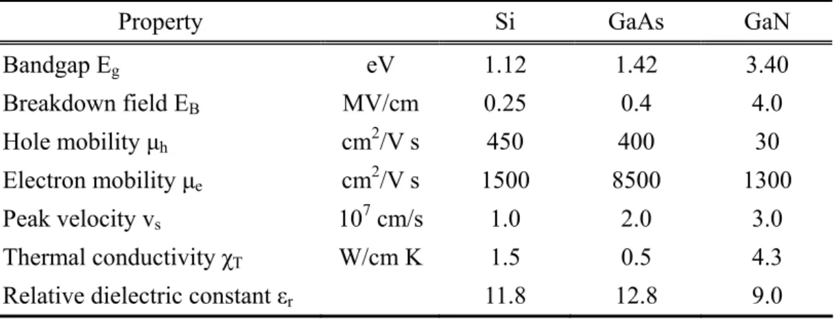
Compared with other semiconductor materials, III-Nitrides are also characterized by other superior properties, such as high breakdown field, high peak velocity of electron carriers, high thermal conductivity [9]-[13]. Table 2.3 shows the comparison of some important characteristics between GaN and other semiconductors. These unique properties make this material suitable for high-power and high-frequency devices particularly operating at elevated temperature.
Table 2.3 Comparison of semiconductor material properties at 300 K
Property Si GaAs GaN
Bandgap Eg eV 1.12 1.42 3.40 Breakdown field EB MV/cm 0.25 0.4 4.0 Hole mobility μh cm2/V s 450 400 30 Electron mobility μe cm2/V s 1500 8500 1300 Peak velocity vs 107 cm/s 1.0 2.0 3.0 Thermal conductivity χT W/cm K 1.5 0.5 4.3
Relative dielectric constant εr 11.8 12.8 9.0
2.1.3 Internal electrical field
An important characteristic of the nitrides that influences the device properties is the presence of strong internal electrical fields inside the epitaxial structures. Wurtzite nitrides have a non-centrosymmetric crystal structure with a polar axis along the c-axis. Therefore, the misfit strain in heterostructures grown along the c-axis can generate an electric moment due to the piezoelectric effect [14]-[16]. In addition to the strain-induced polarization, theory predicts that the spontaneous polarization is very large in the nitrides even if the material is at zero strain [15]. Indeed, the wurtzite structure has the highest symmetry compatible with the existence of spontaneous polarization (or pyroelectric field with reference to its change with temperature) as shown in Fig. 2.3 [17], [18]. The calculated spontaneous polarization for AlN, GaN, and InN is summarized in Table 2.4. According to the calculation, the field resulting from the spontaneous polarization has a fixed orientation which is parallel to the [0001]-direction.
Fig. 2.3 (a) Spontaneous polarization induced by the nonideality of the tetrahedral
structure of GaN; (b) Crystal structure of GaN with Ga-face polarity and spontaneous polarization
Table 2.4 Calculated spontaneous polarization for III-V wurtzite nitrides [15]
AlN GaN InN
Psp C/m2 -0.081 -0.029 -0.032
2.1.4 Polarity
When three of the bonds on a Ga atom with tetrahedral coordination face towards the substrate, the polarity is typically called Ga-face. In contrast, when three bonds face in the growth direction, the material is termed N-face, as shown in Fig. 2.4. There are four possible surface structures in wurtzite III-nitrides, considering both the termination atom and the crystallographic polarity, e.g. Ga-terminated N-face polarity. Although the terms Ga- and N-face, Ga- and N-termination have been used as a sign
of polarity, it is very complicated to distinguish the polarity from the termination atoms, though Seelmann-Eggebert et al. do use ‘termination’ to represent the polarity [19]. Furthermore, since AlN, InN and their alloys also need to be considered, the polar structure with the three bonds of III-atom facing toward the substrate is defined as +c polarity and the opposite as –c polarity.
Fig. 2.4 Schematic illustration of GaN wurtzite crystal structure exhibiting the
polarity along the c-axis. GaN with Ga-face (+c) polarity on left side and GaN with N-face (-c) polarity on right side. When the direction of the three bonds of the III-element is towards the substrate, the polar structure is defended as +c polarity. On the other hand, when that of these bonds are upward against substrate, it is defined as having –c polarity.
Yang et al. exhibited the difference between Ga- and N-face by using UV-photoelectron emission microscopy (PEEM) [20]. It was indicated that the
emission threshold of the N-face region is lower than that of the Ga-face region, and the phenomenon can be explained by the model of the surface band bending induced by the polarization bound surface charges as shown in Fig. 2.5. The much higher threshold energy at Ga-face than N-face surface would make Ga-face more chemical inert than N-face GaN.
Fig. 2.5 Energy band diagrams for (a) Ga-face and (b) N-face GaN. The quantitiesφ,
χs, Eth , and Lsc are the surface electron affinity, work function, photo-threshold
energy, and space charge layer, respectively. The arrows represent the directions of spontaneous polarization, Psp , and the internal electric field, E [20].
2.2 Processing Techniques for III-V Nitride Semiconductors
In order to utilize the excellent properties of III-V nitride semiconductors and fulfill the devices, various processing techniques have been developed specifically for these materials. In this section, these techniques including epitaxy, ohmic contacts formation, and high-density-plasma etching will be introduced.
2.2.1 Epitaxial Growth
III-nitrides decompose into the group-III element and nitrogen before they start to melt because of the extremely high melting temperature. This would make it difficult to grow crystals from the nitrides in the melt. The growth of GaN crystals from gallium solution requires again, high temperature (1400 – 1500oC) and elevated nitrogen vapor pressure (10 kbar). The lateral size of bulk single crystals of GaN is therefore limited to up to several millimeters. The difficulty in the growth of bulk substrate material results in epitaxial growth on foreign substrates like sapphire (α-Al2O3) and silicon carbide (6H-SiC).
The nitride semiconductors grown on sapphire or SiC substrates by metal-organic chemical vapor deposition (MOCVD) are commercially available [21]-[23]. The major precursors include tri-methyl or tri-ethyl forms of Ga, Al, and In. Silane (SiH4)
and Cp2Mg are used as n-type and p-type dopant sources, respectively. The growth
condition is set at the temperature of around 1000oC and under the pressure of about 100 torr. Owing to the lattice mismatch between sapphire substrates and GaN semiconductors, a thin buffer layer is usually grown directly on the substrate at a low temperature of 500oC to serve as a template of nucleation [24]. However, the densities
of the threading dislocations in these materials are still in the range of 109 ~ 1010 cm-2, which is on the order of million times higher than that of other semiconductors, like Si or GaAs. The lateral epitaxial overgrowth (LEO) can be employed to further reduce the dislocation density by about 5 orders [25]-[27]. In addition, a few of bulk GaN substrates with low defects are successfully produced by metal organic hydrogen chloride vapor phase epitaxy [28]-[31].
The growth of the ternary nitrides is more complex than that of GaN. In particular, the growth of InGaN is complicated by numerous problems. Due to the thermal instability of InN, In incorporation is expected to be elevated by the reduction of the growth temperature, which can be achieved at the expense of a diminished crystalline quality. Further more, the large lattice mismatch between InN and GaN produces considerable internal strain in the InGaN alloy due to a crystalline lattice distortion, which leads to phase separation and immiscibility [32]-[35]. The existence of large compositional fluctuation may be encouraged by the miscibility cap in this system [32].
The as-grown p-type GaN layer has very few carriers because the Mg-dopants are trapped by hydrogen atoms which come from the reactive sources and carrier gases. To obtain the real p-type GaN layers, these Mg-H bonds must be broken after an activation process, which is performed by a post thermal annealing at 500 ~ 700oC under a pure nitrogen atmosphere [36]. However, there is only about 1% of the Mg atoms ionized at room temperature owing to the deep acceptor level of around 170 meV above the valence band edge [37]. The typical mobility of holes is as low as 20 cm2/Vs, just allowing the realization of p-n junctions. A record value of 150 cm2/Vs was ever obtained by compensating the scattering atoms [38].
2.2.2 Metal Contacts
Metal-Semiconductor (MS) junctions are of great importance since they are present in every semiconductor device. They can behave either as a Schottky barrier or as an ohmic contact dependent on the characteristics of the interface. Low-resistance, thermally stable ohmic contacts to GaN are crucial for obtaining good performance of light emitting diodes. This section will primarily focus on the formation of ohmic contact on GaN.
Unlike the cases of Si and GaAs, the Fermi level at the interface between the GaN semiconductor and the metal would be unpinned due to the substantial ionic component of the bonds in GaN [39]. Therefore, the Schottky barrier height (eΦb),
which is the difference between the semiconductor band edge and the Fermi level at the junction, can be evaluated as follows.
eΦb = eΦm – eχs, for n-type GaN, (1.3)
eΦb = Eg – (eΦm – eχs), for p-type GaN (1.4)
Where eΦm represents the work function of the contact metal, and eχs (= 4.1eV) is the
electron affinity of GaN.
A metal-semiconductor junction results in an ohmic contact (i.e. a contact with voltage independent resistance) if the Schottky barrier height, Φb, is zero or negative.
In such case, the carriers are free to flow in or out of the semiconductor so that there is a minimal resistance across the contact. For n-type GaN, this means that the work function of the metal must be close to or smaller than the electron affinity of GaN (~ 4.1 eV). For p-type GaN, it requires that the work function of the metal must be close to or larger than the sum of the electron affinity and the bandgap energy. However, the work function of most metals is less than 6 eV, and the sum of the electron affinity and the bandgap energy (~ 3.4 eV) is about 7.5 eV. It can be problematic to find a
metal that provides a good ohmic contact to p-type GaN.
For n-type GaN, choosing the metals of low work functions and increasing the doping concentration of n-type GaN can provide a good ohmic contact. At first, Al and Au ohmic contacts to GaN were used. These contacts yielded specific contact resistances of 10-4 and 10-3 Ωcm2, respectively. [40] The use of Ti in ohmic contacts
to GaN resulted in much smaller contact resistance. Lin et al. [41] described an Al/Ti ohmic contact to n-GaN with a specific contact resistance of 8x10⁻⁶ Ωcm2. Later, Fan
et al. [42] reported on the Al/Ni/Al/Ti contact to n-GaN and obtained the specific ohmic resistance as low as 9x10⁻⁸ Ωcm2 after alloy at a proper temperature. The
mechanism of obtaining such a low contact resistance was shown to be the formation of TiN, which leads to a large concentration of N vacancies (that behave as donors in GaN) near the surface [43]. The dependence of the specific contact resistance on doping was studied by Khan et al. [44]. Wolter et al. [45] studied ZrN/Zr ohmic contact to GaN that showed a promising thermal stability with a reasonable specific contact resistance of 2x10⁻⁵ Ωcm2 for n-GaN with the electron concentration of 7x10¹⁷
cm-3. These contacts exhibited excellent thermal stability in evacuated quartz tubes at 600oC for 1000 hours. Holloway et al. [46] reviewed the results obtained for ohmic contacts to GaN. A low contact metallization for ohmic contacts was reported in [47].
As for p-type GaN, it is a great challenge to form low-resistivity ohmic contacts due to the following reasons.
(a) According to the equation of (1.4), the work function of the metal should be close to 7.5 eV. However, most metal exhibits a work function being lower than 6 eV.
(b) The carrier concentration in p-type GaN is low due to the deep ionization level of the Mg acceptor. There are only 1% of dopants ionized in p-GaN and this low hole concentration can not lead to a tunneling junction at the metal/p-GaN
interface.
(c) There is a tendency for the preferential loss of nitrogen from the GaN surface during processing, which may produce surface conversion to n-type conductivity.
A bilayer metal film of Ni/Au on p-type GaN is most common structure adopted for GaN-based optoelectronic devices. Ni/Au layer is deposited on p-GaN by an e-beam evaporator and subsequently annealed at 500-700°C. The typical contact resistance is around 10-3-10-2 Ωcm2 [48], [49]. Although the contact resistivity is not low enough, it is allowable for application in LEDs. It was also found that the specific contact resistance of Ni/Au could be reduced to 4x10⁻⁶Ωcm2 after annealing in an oxygen ambience [50]-[52], but both the reliability and the reproducibility were disputable [53], [54]. Furthermore, Al0.15Ga0.85N/GaN strained superlattices were fabricated to
enhance the surface carrier concentration, so the contact resistance was reduced effectively with the traditional Ni/Au-contact method [55], [56]
2.2.3 High-density-plasma Dry Etch
Due to the inert properties of III-Nitrides, it is difficult to etch GaN with wet chemicals. It was only found that GaN could be etched at practical rate with molten salts such as KOH or NaOH at temperatures above 250°C. Although the technique of photochemical etching has been developed for nitrides [57], the difficult procedure of adding electrodes to spread current and selectivity over polarity of GaN restricts its application. It is much easier to etch N-polarity than Ga-polarity GaN owing to the much lower photo threshold energy of N-polarity GaN as mentioned in section 1.1.4. However, the epitaxial quality of N-polarity material is always poorer than
Ga-polarity one, and it is necessary to utilize Ga-polarity materials to fabricate devices with high performance.
Dry etching is the most practical and feasible method. Especially, the high-density plasma (HDP) etchers, which use inductively coupled plasma (ICP) or electron cyclotron resonance (ECR) techniques to generate the plasma sources with 1011~1012cm-3 densities, can provide higher etching rates than the typical reactive ion etcher (RIE) without serious damages on the GaN surface [58], [59]. A variety of reactive gases have been investigated for GaN etching. Some special recipes can improve the etching selectivity among different epi-layers [60]. The chlorine-based gas mixtures are usually adopted owing to fair volatilities of gallium chlorides. Methane (CH4) is also added in the mixture in order to etch the epi-layer containing
indium content.
2.3 GaN-based light emitting diodes
In general, one excites electron-hole (e-h) pairs by an external source of energy in a semiconductor, and they are in non-equilibrium state. In most cases, the electrons and holes will relax to quasi-thermal equilibrium distribution through a thermalization process such as carrier-carrier and carrier-phonon interaction. In the final step, the e-h pairs recombine, and their energy is released. Radiative recombination produces emission of photons and the non-radiative recombination release the energy to crystal lattice in the form of heat.
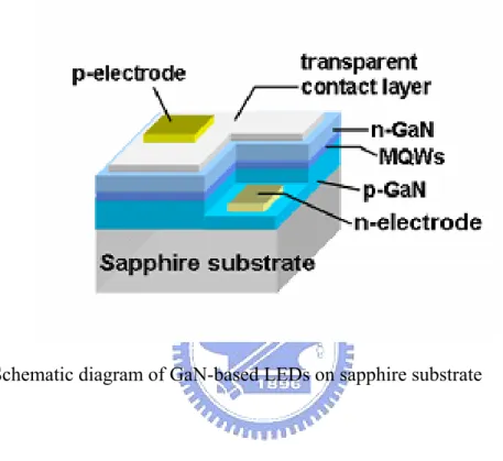
As shown in Fig. 1.6, the GaN-based LED is schematically illustrated. N-type, multi-quantum wells and p-type GaN is epitaxially grown on sapphire substrates in sequence by MOCVD, and processed by dry etching to expose the n-GaN layer
followed by metallization to form the transparent ohmic contacts on p-type GaN as a current spreading layer. P- and n-electrode are both formed on etch type of GaN. Finally, the sapphire substrates were thinned to about 90um by polishing and were scribed and sliced into chips.
Fig. 2.6 Schematic diagram of GaN-based LEDs on sapphire substrate
References
[1] J. H. Edgar, Properties of group III nitrides (INSPEC, IEE, London, 1994). [2] M. Suzuki and T. Uenoyama, J. Appl. Phys., vol. 80, pp. 6868-6874, Dec. 1996. [3] J. W. Orton and C. T. Foxon, Semicond. Sci. Technol., vol. 13, pp. 310-313,
1998.
[4] Z. Dridi, B. Bouhafs, and P. Ruterana, Semicond. Sci. Technol., vol. 18, pp. 850-856, 2003.
[5] S. Strite and H. Morkoc, J. Vac. Sci. Technol. B, vol. 10, pp.1237-1266, Jul/Aug. 1992.
[7] Q. Guo and A. Yoshida, Jpn. J. Appl. Phys., vol. 33, pp. 2453-2456, May 1994. [8] V. Y. Davydov, A. A. Klochikhin, V. V. Emtsev, S. V. Ivanov, V. V. Vekshin, F.
Bechstedt, J. Furthmuller, H. Harima, A. V. Mudryi, A. Hashimoto, A. Yamamoto, J. Aderhold, J. Graul, and E. E. Haller, Phys. Stat. Sol. (b), vol. 230, pp. R4-R6, 2002.
[9] V. W. L. Chin, T. L. Tansley, and T. Osotchan, J. Appl. Phys., vol. 75, pp. 7365-7372, Feb. 1994.
[10] M. Shur, B. Gelmont, and M. A. Khan, J. Electronic Materials, vol. 25, pp. 777-785, May 1996.
[11] K. S. Kim, C. S. Oh, W. -H. Lee, K. J. Lee, G. M. Yang, C. -H. Hong, E. -K. Suh, K. Y. Lim, H. J. Lee, and D. J. Byun, J. Crystal Growth, vol. 210, pp. 505-510, 2000.
[12] B. E. Foutz, S. K. O’Leary, M. S. Shur, and L. F. Eastman, J. Appl. Phys., vol. 85, pp.7727-7734, Jun. 1999.
[13] W. J. Fan, M. F. Li, T. C. Chong, and J. B. Xia, Solid State Communications, vol. 97, pp. 381-384, 1996.
[14] A. Bykhovski, B. Gelmont, and M. Shur, J. Appl. Phys., vol. 74, pp. 6734-6739, Dec. 1993.
[15] F. Bernardini, V. Fiorentini, and D. Vanderbilt, Phys. Rev. B, vol. 56, pp. R10024-R10027, Oct. 1997.
[16] C. Kisielowski, J. Kruger, S. Ruvimov, T. Suski, J. W. Ager III, E. Jones, Z. Liliental-Weber, M. Rubin, E. R. Weber, M. D. Bremser, and R. F. Davis, Phys. Rev. B, vol. 54, pp. 17745-17753, Dec. 1996.
[17] J. F. Nye, Physical properties of crystals (Clarendon Press, Oxford, 1995).
[18] O. Gfrorer, C. Gemmer, J. Off, J. S. Im, F. Scholz, and A. Hangleiter, Phys. Stat. Sol. (b), vol. 216, pp. 405-408, 1999.
[19] M. Seelmann-Eggebert, J. L. Weyher, H. Obloh, H. Zimmermann, A. Rar, and S. Porowski, Appl. Phys. Lett., vol. 71, pp. 2635-2637, Nov. 1997.
[20] W.-C. Yang, B. J. Rodriguez, M. Park, R. J. Nemanich, O. Ambacher and V. Cimalla, J. Appl. Phys., vol. 94, pp. 5720-5725, Nov. 2003.
[21] S. Nakamura, Jpn. J. Appl. Phys., vol. 30, pp. L1705-L1707, Oct. 1991.
[22] Q. Guo, O. Kato, and A. Yoshida, J. Appl. Phys., vol. 73, pp. 7969-7971, Jun. 1993.
[23] O. Ambacher, M. S. Brandt, R. Dimitrov, T. Metzger, M. Stutzmann, R. A. Fischer, A. Miehr, A. Bergmaier, and G. Dollinger, J. Vac. Sci. Technol. B, vol. 14, pp. 3532-3542, Nov/Dec. 1996.
[24] H. Amano, N. Sawaki, I. Akasaki, and Y. Toyada, Appl. Phys. Lett., vol. 48, pp. 353-355, Feb. 1986.
[25] D. Kapolnek, S. Keller, R. Vetury, R. D. Underwood, P. Kozodoy, S. P. Den Baars, and U. K. Mishra, Appl. Phys. Lett., vol. 71, pp. 1204-1206, Sep. 1997. [26] X. Li, A. M. Jones, S. D. Roh, D. A. Turnbull, S. G. Bishop, and J. J. Coleman, J.
Electronic Materials, vol. 26, pp. 306-309, 1996.
[27] G. Nataf, B. Beaumont, A. Bouille, P. Vennegues, S. Haffouz, M. Vaille, P. Gibart, Materials Science and Engineering: B, vol. 59, pp. 112-116, 1999.
[28] S. Kurai, Y. Naoi, T. Abe, S. Ohmi, and S. Sakai, Jpn. J. Appl. Phys., vol. 35, pp. L77-L79, Jan. 1996.
[29] S. Porowski, J. Crystal Growth, vol. 166, pp. 583-589, 1996.
[30] M. K. Kelly, R. P. Vaudo, V. M. Phanse, L. Gorgens, O. Ambacher, and M. Stutzmann, Jpn. J. Appl. Phys., vol. 38, pp. L217-L219, Mar. 1999.
[31] Y. Kumagai, H. Murakami, A. Koukitu, K. Takemoto, and H. Seki, Jpn. J. Appl. Phys., vol. 39, pp. L703-L706, Jul. 2000.
1996.
[33] N. A. El-Masry, E. L. Piner, S. X. Liu, and S. M. Bedair, Appl. Phys. Lett., vol. 72, pp. 40-42, Jan. 1998.
[34] R. Singh, R. J. Molnar, M. S.Unlu, and T. D. Moustakas, Appl. Phys. Lett., vol. 64, pp. 336-338, Jan. 1994.
[35] S. Y. Karpov, MRS Internet J. Nitride Semicond. Res., vol. 3, pp. 1-5, 1998. [36] S. Nakamura, T. Mukai, M. Senoh, N. Iwasa, Jpn. J. Appl. Phys., vol. 31, pp.
L139-L142, Feb.1992.
[37] D. J. Kim, D. Y. Ryu, N. A. Bojarczuk, J. Karasinski, S. Guha, S. H. Lee, and J. H. Lee, J. Appl. Phys., vol. 88, pp. 2564-2569, Sep. 2000.
[38] O. Brandt, H. Yang, H. Kostial, and K. Ploog, Appl. Phys. Lett. vol. 69, pp. 2707-2709, Oct. 1996.
[39] S. Kurtin, T. C. McGill, and C. A. Mead, Physical Review Letters, vol. 22, pp. 1433-1436, Jun. 1969.
[40] J. S. Foresi and T. D. Moustakas, Appl. Phys. Lett., vol. 62, pp. 2859-2861, May 1993.
[41] M E. Lin, Z. Ma, F. Y. Huang, Z. F. Fan, L. H. Allen, and H. Morkoc, Appl. Phys. Lett., vol. 64, pp. 1003-1005, Feb. 1994.
[42] Z. F. Fan, S. N. Mohammad, W. Kim, O. Aktas, A. E. Botchkarev, and H. Morkoc, Appl. Phys. Lett., vol. 68, pp. 1672-1674, Mar. 1996.
[43] S. Ruvimov, Z. Liliental-Weber, J. Washburn, K. J. Duxstad, E. E. Haller, Z. -F. Fan, S. N. Mohammad, W. Kim, A. E. Botchkarev, and H. Morkoc, Appl. Phys. Lett., vol. 69, pp. 1556-1558, Sep. 1996.
[44] M. A. Khan, M. S. Shur, and Q. Chen, Appl. Phys. Lett., vol. 68, pp. 3022-3024, May 1996.
Electrochemical and Solid-State Letters, vol. 2, pp. 151-153, 1999.
[46] P. H. Holloway, T. -J. Kim, J. T. Trexler, S. Milla, J. J. Fijol, W. V. Lampert, and T. W. Haas, Appl. Surface Science, vol. 117/118, pp. 362-372, 1997.
[47] D. Qiao, Z. F. Guan, J Carlton, S. S. Lau, G. J. Sullivan, Appl. Phys. Lett., vol. 74, pp. 2652-2654, May 1999.
[48] J. -L. Lee, J. K. Kim, J. W. Lee, Y. J. Park, and T. Kim, Solid-State Electronics, vol. 43, pp. 435-438, Feb. 1999.
[49] J. K. Sheu, Y. K. Su, G. C. Chi, W. C. Chen, C. Y. Chen, C. N. Huang, J. M. Hong, Y. C. Yu, C. W. Wang, and E. K. Lin, J. Appl. Phys., vol. 83, pp. 3172-3175, Mar. 1998.
[50] J. -K. Ho, C. -S. Jong, C. C. Chiu, C. -N. Huang, C. -Y. Chen, and K. -K. Shih, Appl. Phys. Lett., vol. 74, pp. 1275-1277, Mar. 1999.
[51] L. -C. Chen, J. -K. Ho, C. -S. Jong, C. C. Chiu, K. -K. Shih, F. -R. Chen, J. -J. Kai, L. Chang, Appl. Phys. Lett., vol. 76, pp. 3703-3705, Jun. 2000.
[52] L. -C. Chen, F. -R. Chen, J. -J. Kai, L. Chang, J. -K. Ho, C. -S. Jong, C. C. Chiu, C. -N. Huang, C. -Y. Chen, and K. -K. Shih, J. Appl. Phys., vol. 86, pp. 3826-3832, Oct. 1999.
[53] T. Maeda, Y. Koide, and M. Murakami, Appl. Phys. Lett., vol. 75, pp. 4145-4147, Dec. 1999.
[54] H. Kim, D. -J. Kim, S. -J. Park, and H. Hwang, J. Appl. Phys., vol. 89, pp. 1506-1508, Jan. 2001.
[55] C. H. Kuo, J. K. Sheu, G. C. Chi, Y. L. Huang, T. W. Yeh, Solid-State Electronics, vol. 45, pp. 717-720, May 2001.
[56] J. K. Sheu, G. C. Chi, and M. J. Jou, IEEE Electron Device Letters, vol. 22, pp. 160-162, Apr. 2001.
Oct. 1997.
[58] S. J. Pearton, Materials Science and Engineering: B, vol. 40, pp. 101-118, 1996. [59] R. J. Shul, G. A. Vawter, C. G. Willison, M. M. Bridges, J. W. Lee, S. J. Pearton,
and C. R. Abernathy, Solid-State Electronics, vol. 42, pp. 2259-2267, Dec. 1998. [60] R. J. Shul, C. G. Willison, M. M. Bridges, J. Han, J. W. Lee, S. J. Pearton, C. R.
Abernathy, J. D. Mackenzie, and S. M. Donovan, Solid-State Electronics, vol. 42, pp. 2269-2276, Dec. 1998.
Chapter 3
Highly Reliable GaN-Based Light-Emitting Diodes
Formed by p-In
0.1Ga
0.9N/ITO Structure
3.1 Introduction
Group III-Nitride semiconductors have attracted much attention for their versatile applications recently [1], [2]. A high-brightness GaN-based light emitting diode is an interesting issue because of its important role in full-color display and lighting applications [3], [4]. Following the successful demonstration of p-type conductivity on Mg-doped GaN by post-growth thermal annealing in nitrogen ambience, blue and green LEDs become real and commercially available [5]. However, poor conductivity of p-GaN layer still limits the current spreading, and it is necessary to deposit a conductive layer for current spreading. This layer should not only form good ohmic contacts to p-GaN but also be transparent to the emitted light from the active layer. In the past, much work focused on materials and methods to form good contacts to p-GaN [6]-[8]. Among these studies, Ni/Au is usually used as a semi-transparent current spreading layer due to its good contact characteristics. However, Sheu et al. [9] showed that the transmittance of semi-transparent Ni/Au films for blue LEDs is only about 60% to 85% in the 450-550 nm wavelengths. To improve the transmittance, it is feasible to replace the conventional Ni/Au contact by a better transparent conductive contact. Nowadays transparent conductive oxide materials (TCO), such as indium-tin-oxide (ITO), aluminum-doped-zinc-oxide (AZO)
and cadmium-tin-oxide (CTO), are widely applied to optical electrical devices [10], [11]. There are also several studies [12]-[15] discussing the applications of ITO to GaN-based LEDs. Margalith et al. [12] obtained the Schottky but not Ohmic characteristics of the ITO/p-GaN interface after thermal annealing. This result could be attributed to a large work function difference between ITO and p-GaN. In order to improve the contact characteristics, some authors added an interfacial layer such as Ni or NiO before ITO deposition by a little sacrifice of transparency [13]-[15]. In this chapter, we demonstrate a thin p-In0.1Ga0.9N layer as an intermediate between ITO
and p-GaN to form a nearly ohmic contact. The LEDs with this structure exhibit excellent reliability under a 50-mA current stress.
3.2 Experimental
The InGaN–GaN multi-quantum-wells (MQWs) LED wafers were grown on c-face sapphire substrates by a metal-organic chemical vapor deposition (MOCVD) system. The epitaxial structure comprised 4-μm-thick n-GaN, 0.1-μm-thick InGaN–GaN (MQWs) active layer, and 0.1-μm-thick p-GaN, as shown in Fig. 3.1 (1). Moreover, the carrier concentrations of the p-GaN and n-GaN were 5 x 1017 cm-3 and 3 x 1018 cm-3, respectively. A wafer with a peak wavelength at 465 nm was chosen and cut into 4 pieces. One piece was prepared for the conventional LEDs with Ni/Au contact, and the other three were re-loaded into the same MOCVD chamber to grow a 10-nm-thick p-In0.1Ga0.9N layer for LEDs with ITO contacts.
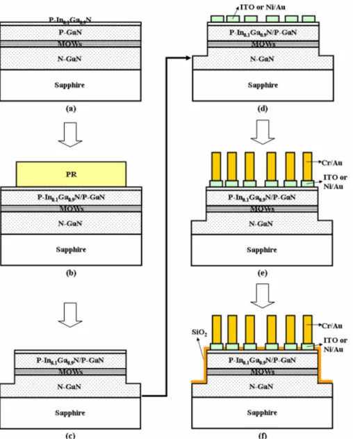
GaN-based LEDs (300 μm x 300 μm) and the corresponding transmission line model (TLM) structures for p-type ohmic contact characterization with different conducting layers were fabricated as shown in Fig. 3.1. First, inductance coupled
plasma (ICP) etcher was used to form mesa structures and then these samples were immersed in H2SO4:H2O2 and NH4OH:H2O solutions to remove resist and native
oxides. Next, ITO (280 nm) was deposited on the p-In0.1Ga0.9N/p-GaN samples by
E-beam evaporator at 300oC in oxygen ambience with a partial pressure of 5 x 10⁻⁴ Torr, and the Ni/Au (4 nm/4 nm) was deposited on the p-GaN sample by E-beam evaporator with a base pressure of 2 x 10⁻⁶ Torr. The p-In0.1Ga0.9N/ITO contact
samples were subsequently annealed at 500oC and 600oC in nitrogen ambience. As for the Ni/Au contact sample, it was annealed at 540oC in nitrogen ambience to achieve the optimal ohmic contact to p-GaN. Cr/Au (0.08 μm/0.8 μm) metallization was employed for the n-type contact layer, p- and n- bonding pads. TLM structures were used to measure the contact resistivity of the conducting layers on p-GaN. The pad size is 300 μm x 80 μm and the spacings were 2, 3, 4, 6, 8, 15 and 20 μm. The current-voltage characteristics were measured at room temperature by an HP-4156 analyzer with a current source.
After measuring, these samples were subsequently polished, scribed and sliced into chips. We chose 10 chips per sample to package into TO-Can forms. A Keithley 2430 source meter was connected with an integrating sphere to measure the current-voltage and current-power characteristics of these LEDs. During the reliability testing, these chips with TO-Can form were stressed by a 50-mA current injection at room temperature and relative humidity of 40%.
In order to truly exhibit the effects of absorption, internal reflection and interference of the conducting films on GaN-based LEDs, the p-i-n GaN with a double-side-polished sapphire substrate was used in the transmittance measurement. The transmittance spectra of these samples were measured by Hitachi U3010 spectrophotometer.
Fig. 3.1 The process flow diagrams of (a) GaN-based LEDs fabrication and (b) TLM
structure formation: (1) epitaxial structure (2) lithographic patterning (3) ICP etching to expose n-GaN layer (4) ITO deposition and patterning, (5) bonding pads metallization (6) SiO2 protection layer.
3.3 Results and Discussion
Figure 3.2 shows the transmittance of the p-i-n GaN/sapphire, ITO and Ni/Au layers deposited on p-i-n GaN/sapphire samples with different annealing temperatures. Due to the great difference of optical index between GaN and air, the blank sample with p-i-n GaN/sapphire structure exhibits relatively poor transmittance. The curves of ITO samples annealed at 500oC and 600oC are nearly coincident, and the light transmittance at 465 nm is 83% while Ni/Au sample shows only 61% due to the high extinction coefficient of Ni and Au. It is supposed that ITO can extract more light than the conventional Ni/Au layer does.
350 400 450 500 550 600 650 700 750 0 20 40 60 80 100 T ran sm ittan c e (% ) Wavelength (nm) ITO, 500oC ITO, 600oC Ni/Au, 540oC p-i-n GaN/Sapphire
Fig. 3.2 Transmittance spectra of the blank p-i-n GaN/sapphire, the ITO and Ni/Au
films deposited on p-i-n GaN/sapphire under different annealing conditions. (nITO@ 470 nm = 1.8, nGaN@ 470 nm = 2.5)
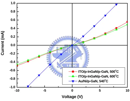
Figure 3.3 presents the current-voltage characteristics of different contacts on p-GaN. The Ni/Au sample exhibits a linear ohmic property, while the sample of p-In0.1Ga0.9N/ITO shows a nearly linear ohmic characteristic after annealed at the
temperature of 500oC, which is the optimal condition.
-10 -5 0 5 10 -1.0 -0.8 -0.6 -0.4 -0.2 0.0 0.2 0.4 0.6 0.8 1.0 C u rr en t (m A ) Voltage (V) ITO/p-InGaN/p-GaN, 500oC ITO/p-InGaN/p-GaN, 600oC Au/Ni/p-GaN, 540oC
Fig. 3.3 I-V characteristics of p-In0.1Ga0.9N/ITO contacts annealed at 500oC, 600oC
and Ni/Au contact annealed at 540oC on p-GaN. (The spacing between two electrodes is 2 um)
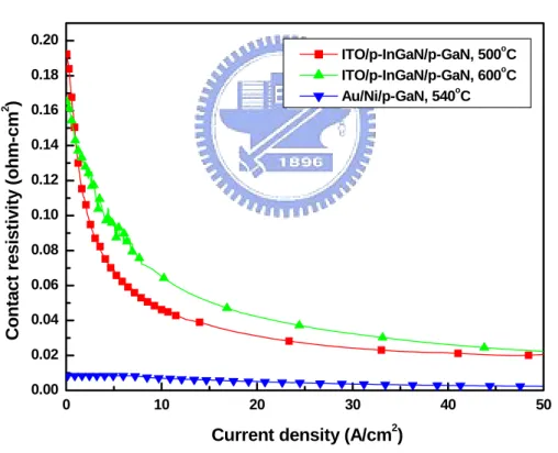
As shown in Fig. 3.4, the contact resistivity of Ni/Au contact decreases from 8 x 10⁻³ ohm-cm2 to 3 x 10⁻³ ohm-cm2 with increasing the current density from 0 to 50 A-cm-2. As for the p- In0.1Ga0.9N/ITO contact samples, the contact resistivity reduces
from 2 x 10⁻¹ ohm-cm2 to 2.5 x 10⁻² ohm-cm2 with raising the current density from 0 to 50 A-cm-2. The results imply that both the interfaces of p-GaN with Ni/Au and p-In0.1Ga0.9N/ITO contacts are not ideal ohmic contacts, but the former exhibits better
contact property than the latter. Moreover, this figure also indicates that the contact resistivity is 2.6 x 10⁻² ohm-cm2 under a current density of 27 A-cm-2, which is equivalent to a current of 20 mA applied during the normal LED operation. This result shows that the p-In0.1Ga0.9N/ITO contact is good enough to be used in LED
application. 0 10 20 30 40 50 0.00 0.02 0.04 0.06 0.08 0.10 0.12 0.14 0.16 0.18 0.20 C o n ta c t r e si s ti v ity (o h m -cm 2 )
Current density (A/cm2)
ITO/p-InGaN/p-GaN, 500oC
ITO/p-InGaN/p-GaN, 600oC
Au/Ni/p-GaN, 540oC
Fig. 3.4 Contact resistivities as functions of injection current density.
and the dynamic resistance decreases with elevating the injected current. At the current of 20 mA, the forward voltage and the dynamic resistance are 3.43 V and 17.1 ohm chips with p-In0.1Ga0.9N/ITO contacts annealed at 500oC, respectively. On the
other hand, the conventional chips with Ni/Au contacts show 3.21 V and 14.8 ohm. The ITO contact LEDs exhibit a little bit higher but acceptable forward voltage and dynamic resistance by 0.2 V and 2.3 ohm in comparison with the conventional Ni/Au contact LEDs. 0 20 40 60 80 100 2 3 4 5 For w ar d Vol ta ge ( V )
Forward Current (mA)
0 20 40 60 80 100 120 ITO LED, 500oC ITO LED, 600oC Ni/Au LED, 540oC Dynam ic Re si s ta nce (ohm )
Fig. 3.5 The forward voltage and dynamic resistance as functions of injection
current of GaN-based LEDs with p-In0.1Ga0.9N/ITO and Ni/Au contacts.
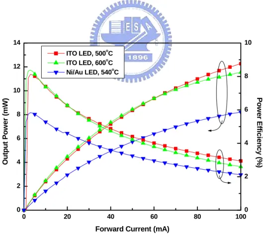
Figure 3.6 shows the optical properties of LEDs with different contacts. The output power increases with raising the injected current. But the power efficiency of
ITO contacts and Ni/Au contacts LEDs has a maximum value of 8.12% and 5.83% at 3-mA-current injection, respectively, and then decreases with elevating the injected current. At the current of 20 mA, the output power and power efficiency are 4.30 mW and 6.26% for chips with 500oC-annealed p-In0.1Ga0.9N/ITO contacts in
comparison with that of 2.95 mW and 4.60% for the conventional Ni/Au contacts LEDs. It is estimated that LEDs with p-In0.1Ga0.9N/ITO contacts can enhance the
external quantum efficiency and power efficiency by about 46% and 36% at 20 mA, respectively. This improvement is definitely attributed to the high transparent contacts and relatively low contact resistance. The electrical and optical characteristics of LEDs with ITO contacts are summarized in table 3.1 compared with the previous works. 0 20 40 60 80 100 0 2 4 6 8 10 12 14 ITO LED, 500oC ITO LED, 600oC Ni/Au LED, 540oC Output Pow e r ( m W )
Forward Current (mA)
0 2 4 6 8 10 Pow e r Eff ici ency ( % )
Fig. 3.6 The output power and power efficiency as functions of injection current of
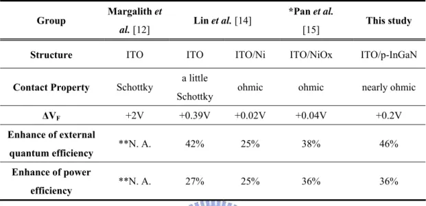
Table 3.1 GaN-based LEDs of different ITO contacts are compared with that of
Ni/Au contact.
Group Margalith et
al. [12] Lin et al. [14]
*Pan et al.
[15] This study
Structure ITO ITO ITO/Ni ITO/NiOx ITO/p-InGaN
Contact Property Schottky a little
Schottky ohmic ohmic nearly ohmic
ΔVF +2V +0.39V +0.02V +0.04V +0.2V
Enhance of external
quantum efficiency **N. A. 42% 25% 38% 46%
Enhance of power
efficiency **N. A. 27% 25% 36% 36%
* Data from Pan et al. is compared with Ni/Au oxides contacts. ** N. A. means “Not Available”.
From the results of life test shown in Fig. 3.7, the conventional Ni/Au samples would suffer the output power decay of 27% after 1008-hour stress and the 500oC-annealed ITO samples showed a similar decay of 25%. However, the light power was deteriorated by 36% for the p-In0.1Ga0.9N/ITO samples annealed at 600oC.
This result is probably due to the poor contact property which will induce a severe heating effect under high current injection. Besides, the surface morphology of 600oC
0 200 400 600 800 1000 -80 -70 -60 -50 -40 -30 -20 -10 0 Deg rad at ion o f O ut p u t P ow er ( % ) Time (hour) ITO LEDs, 500oC ITO LEDs, 600oC Conventional LEDs
Fig. 3.7 Room temperature life test of degradation of output power from GaN-based
LEDs with p-In0.1Ga0.9N/ITO and Ni/Au contacts.
3.4 Summary
This chapter presented highly transparent and nearly ohmic contacts of p-In0.1Ga0.9N/ITO on p-GaN and exhibited the excellent reliability of the
p-In0.1Ga0.9N/ITO contact LEDs. The contact resistivity is 2.6 x 10⁻² ohm-cm2 at a
current density of 27 A-cm-2, and this value is low enough for the application of LEDs. GaN-based LEDs with p-In0.1Ga0.9N/ITO contacts were also fabricated and the
forward voltage was 3.43 V at a current injection of 20 mA. Although the forward voltage was a little higher than the conventional LEDs by 0.2 V, the external quantum
![Table 2.1 Lattice constants of wurtzite nitrides at room temperature [3]. For an ideal closed packed hexagonal structure c/a=1.633 and u=0.375](https://thumb-ap.123doks.com/thumbv2/9libinfo/8747485.205238/25.892.179.713.1000.1147/table-lattice-constants-wurtzite-nitrides-temperature-hexagonal-structure.webp)
![Table 2.4 Calculated spontaneous polarization for III-V wurtzite nitrides [15]](https://thumb-ap.123doks.com/thumbv2/9libinfo/8747485.205238/29.892.144.715.550.765/table-calculated-spontaneous-polarization-iii-v-wurtzite-nitrides.webp)