國 立 交 通 大 學
電子工程學系 電子研究所
碩士論文
高含氮氧化層介面層於二氧化鉿閘極介電層之金氧半
場效電晶體特性研究
Study on high nitrogen concentration oxynitride
as interfacial layer with HfO
2gate dielectric
MOSFETs
研 究 生:簡嘉宏 Jia-Hong Jane
指導教授:羅正忠 博士 Dr.Jen-Chung Lou
高含氮氧化層介面層於二氧化鉿閘極介電質之金氧半
場效電晶體特性研究
Study on high nitrogen concentration oxynitride
as interfacial layer with HfO
2gate dielectric
MOSFETs
研 究 生:簡嘉宏
Student:Jia-Hong Jane
指導教授:羅正忠 博士 Advisor:Dr.Jen-Chung Lou
國 立 交 通 大 學
電子工程學系 電子研究所碩士班
碩 士 論 文
A Thesis
Submitted to
Department of Electronics Engineering & Institute of Electronics
College of Electrical and Computer Engineering
National Chiao Tung University
In Partial Fulfillment of the Requirements
For the Degree of Master of Science
In
Electronic Engineering
August 2008
Hsinchu, Taiwan, Republic of China
高含氮氧化層介面層於二氧化鉿閘極介電層之
金氧半場效電晶體特性研究
研究生:簡嘉宏 指導教授:羅正忠 博士 國立交通大學 電子工程學系 電子研究所碩士班 摘要 隨著互補式金氧半場效電晶體元件尺寸的微縮,傳統的絕緣層-二氧化矽 將遭遇漏電流過大的物理限制。因此,新的絕緣層是往後超大型積體電路發展極 需解決的問題。近年來,高介電常數介電層的技術發展,已成為半導體產業最重 要的研究之一。本篇文章利用高介電常數介電層在相同的等效二氧化矽厚度下, 擁有較大的實際物理厚度以抵擋直接穿隧的漏電流。 此篇文章主要是探討以二氧化鉿堆疊式閘極金氧半場效電晶體,並搭配不 同於一般傳統在高溫下通氧化氮氣體所形成的氮氧化矽介面層,而是利用創新製 程的氮氧化矽作為閘極介電層與矽基板間的介面層。在先前的報告已指出,含氮 氧化層擁有許多傳統氧化層所沒有的優點,例如,有好的抵抗硼擴散的能力、能 有效防禦高電場所造成的熱載子破壞、有較高的介電強度等優點。此外,應用二 氧化鉿作為閘極介電層也有許多優點,例如良好的高溫熱穩定性、且有比氮氧化矽還要高的介電係數、有效降低漏電流等。 我們提出了創新的製程,使得在二氧化鉿閘極介電層與氮氧化矽介面層的 介面上擁有高含量的氮元素,更能有效的去抵擋硼的擴散。形成此堆疊式閘極介 電層有三步驟,首先把晶片浸泡於雙氧水中,形成化學氧化層,之後利用低壓水 平爐管,通氨氣去執行氮化,即完成氮氧化矽介面層,最後再疊上二氧化鉿閘極 介電層即完成。經過以上步驟,就可以在介面上形成高氮含量層,此法製程簡單 與目前的製程技術是相容的。 最後,我們會將此含氮氧化層應用在高介電常數閘極介電層之N型金氧半 場效電晶體上,並使用不同的高介電常數閘極介電層熱退火溫度製程為比較樣 本,探討它們的電性及可靠度,發現較高的高介電常數熱退火溫度樣本擁有比較 高的驅動電流及良好的抵抗定電壓應力的能力。
Study on high nitrogen concentration oxynitride
as interfacial layer with HfO
2gate dielectric
MOSFETs
Student:Jia-Hong Jane Advisor:Dr. Jen-Chung Lou
Department of Electronics Engineering &Institute of Electronics College of Electrical and Computer Engineering
National Chiao-Tung University
Abstract
As the complementary metal-oxide-semiconductor field effective transistor continuously scaling down, conventional isolation layer-SiO2 will experience the larger leakage current physical limit. Therefore, developing the new advanced isolation layer is the biggest problem for the ultra large scale integrated circuits. In recent years, high-K dielectrics layer is one of the most important research for semiconductor industry. In this thesis, we use the high-K dielectric layer has thicker physical thickness under the same effective oxide thickness to avoid direct tunneling leakage current.
In this thesis, we discuss about the HfO2 gate stack metal-oxide-semiconductor
interfacial layer between gate dielectric and silicon substrate instead of using conventional oxynitride as interfacial layer under N2O purging at high temperature.
Oxynitirde(SiON) have been reported to show many advantages over conventionally thermal oxide. For example, excellent resistance to penetration of boron、enhanced endurance to hot carrier damage under high electron field and higher dielectric intensity. Besides, using HfO2 as gate dielectric has many advantages, for example:
excellent thermal stability、higher dielectric constant than oxynitride and effectively decreasing leakage current.
We proposed an alternative approach for forming a high-nitrogen concentration between HfO2 gate dielectric and oxynitride interfacial layer, and be capable of
resisting boron penetration effectively. The forming of this gate stack included three process stages, first step: put the wafers into H2O2 tank to form chemical oxide, and
then the chemical oxide was nitrided using a furnace in low-pressure NH3 ambient to
complete oxynitride interfacial layer. Finally, we deposited HfO2 gate dielectric to
complete this gate stack. During the process mentioned before, we can obtain high nitrogen concentration at the interface. The process proposed here is simple and fully compatible with current process technology.
Finally, we applied the oxynitride to high-K gate dielectric nMOSFETs with different high-K RTA temperature, and discuss about the electric characteristics and
reliability issue, we found that the higher high-K RTA temperature sample has better performance on the driving current and excellent resistance to CVS(constant voltage stress).
誌謝
在兩年碩士生活,在轉眼間就過去了,時間過得非常地快,很快
就要跟學校說再見了,雖然沒什麼時間再見面,謹在此表達我對你們
想說的話。首先,我要感謝我的指導教授羅正忠博士,因為老師的指
導,使我學習到許多研究方法以及為人處世的態度。再來感謝柏村、
永裕、智仁學長,為實驗室盡心盡力,讓我們受益良多。同時,也要
謝謝同在實驗室努力的同學、學弟們:信富、佳樺、土豆、元愷、晨
修、岳展、小陸、翊裳、哲輔,有了你們的陪伴以及幫忙,讓我在實
驗上能夠解決許多的問題及困難。接著,我要感謝一路相伴的蕙,默
默地照顧我、支持我、鼓勵我,雖然我沒什麼時間陪妳,但你總是很
體諒我,謝謝妳。最後,我要感謝的我的家人,在生活上能夠給我無
微不至的照顧,有了你們,才有今天的我。最後感謝主,讓我一次就
跑完實驗以及順利的畢業。
Contents
Abstract(Chinese)---I
Abstract(English)---III
Acknowledgment (Chinese)---VI
Content---VII
Table Captions---IX
Figure Captions---X
Chapter.1 Introduction
1.1 Background---1
1.2 The problems between interfacial layer and HfO
2dielectric---4
1.3 Effects of post-deposition-annealing on HfO
2---4
1.4 Organization of This Thesis---5
Chapter.2 Electrical Characteristics of nMOSFETs with
Oxynitride and HfO
2gate stack
2.1 Introduction---10
2.2 Experiment--- ---12
2.2-1 Experiment procedure---12
2.2-2 Measurement setup---14
2.3-1 Electrical characteristics of nMOSFETs with different High-K RTA temperature---16 2.3-2 Conduction mechanism of nMOSFETs with Oxynitride and HfO2 gate
stack---18
2.4 Summary---21
Chapter.3 Reliability characteristics of nMOSFETs with
Oxynitride and HfO
2gate stack
3.1 Introduction---39
3.2 Measurement setup---40
3.3 Reliability of device with different High-K RTA temperature----41
3.3-1 CVS of devices with different High-K RTA temperature---41 3.3-2 PBTI of devices with different High-K RTA temperature---43
3.4 Summary--- ---44
Chapter.4 Conclusion and future work
4.1 Conclusion--- 54
4.2 Suggestion of Future Work--- 55
Table Captions
Chapter1
Table 1-1 2005 International Technology Roadmap for Semiconductors.---9 The color shade means the solution known and unknown for physics limit.
Chapter2
Figure Captions
Chapter1
Fig. 1-1 High resolution electron microscope images of HfO2/SiO2/Si stack deposited
at (a) 430℃ and (b) 550℃. The zone axis is the [011] direction.---7 Fig. 1-2 XRD pattern of the as-grown and annealed HfO2 films at various
temperature for 3min O2 ambient. The letters m and t represent the
monoclinic and tetragonal structure of the HfO2 film, respectively.---8
Fig. 1-3 Cross-sectional SEM images of (a) the as-grown and (b) the HfO2 film annealed at 800℃.---8
Chapter2
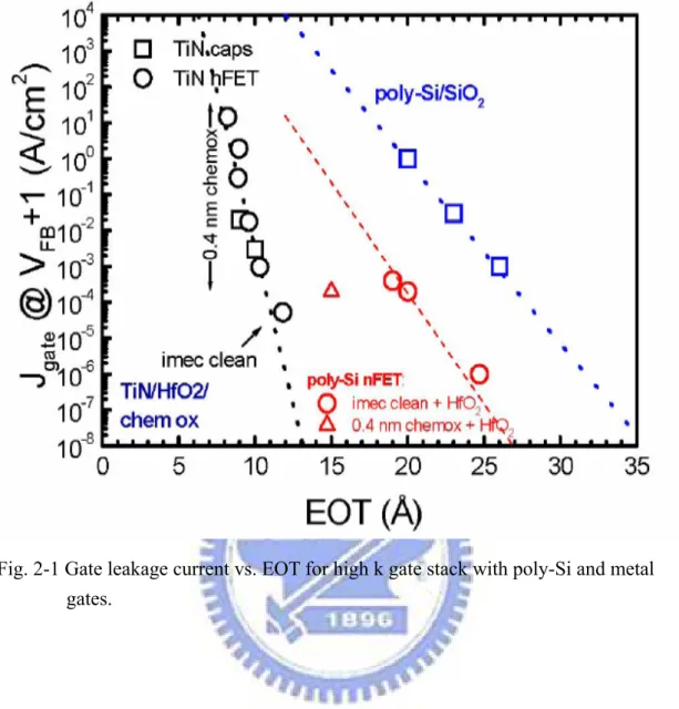
Fig. 2-1 Gate leakage current vs. EOT for high k gate stack with poly-Si and metal gates.---23 Fig. 2-2 The process flow of nMOSFETs with HfO2/SiON gate stack.---24
Fig. 2-3 Schematic cross-section of nMOSFETs with HfO2/SiON gate stack.---24
Fig. 2-4 Basic experimental set-up of charging pumping measurement for
nMOSFETs.---25 Fig. 2-5 Configuration for (a)gate-to-channel, and (b)gate-to-substrate capacitance
measurement.---26 Fig. 2-6 C-V curves for nMOSFETs.---27 Fig. 2-7 Id-Vg & Gm-Vg characteristics of devices with different RTA temperature.28 Fig. 2-8 Id-Vd characteristics fro devices with different RTA temperature.---28
Fig. 2-9 Compared Idlinear with channel length for device with different RTA
temperature.---29 Fig. 2-10 Compared Gmmax with different channel length for device with different
RTA temperature.---29 Fig. 2-11 Compared Gmmax with channel width for device with different RTA
temperature.---30 Fig. 2-12 Compared Gmmax with area for device with different RTA temperature.----30
Fig. 2-13Charge pumping current for device with 600℃ RTA temperature sample-31 Fig. 2-14 Charge pumping current for device with 900℃ RTA temperature sample-31 Fig. 2-15 Compared charge pumping current for device with different RTA
temperature.---32 Fig. 2-16 Compared electron mobility with effective field for device with different
RTA temperature.---32 Fig. 2-17 Carrier separations with 600℃ RTA temperature sample under (a) inversion
(b) accumulation region.---33 Fig. 2-18 Carrier separations with 900℃ RTA temperature sample under (a) inversion (b) accumulation region.---34 Fig. 2-19 n+-gated nMOSFET with HfO2/SiON gate stack under inversion region (a)
band diagrams, and (b) Schematic illustration of carrier separation
experiment.---35 Fig. 2-20 n+ -gated nMOSFET with HfO2/SiON gate stack under accumulation region
(a)band diagrams , and (b)Schematic illustration of carrier separation
experiment.---36 Fig. 2-21 Gate leakage current versus gate bias for device with 600℃ RTA
temperature.---37 Fig. 2-22 Gate leakage current versus gate bias for device with 900℃ RTA
temperature.---38
Chapter3
Fig. 3-1 Basic measurement method for (a) CVS (constant voltage stress), and (b) PBTS (negative bias temperature stress).---45 Fig. 3-2 Id-Vg characteristics for n+-gated nMOSFETs before and after stress 1000s at
25℃ (a) 600℃ sample, and (b) 900℃ sample.---46 Fig. 3-3 Fig. 3-3 Threshold voltage shift as a function of stress time, stressed at 25℃,
Vg=2~3V in linear scale (a) 600℃ sample, and (b) 900℃ sample.---47 Fig. 3-4 Fig. 3-4 Interface trap density shift increase as a function of stress time (a)
600℃ sample, and (b) 900℃ sample.---48 Fig. 3-5 Compared of CVS measurement for devices with different RTA temperature
(a) threshold voltage shift (b) interface trap density shift as a function of stress time.---49 Fig3-6 Id-Vg characteristics for n+-gated nMOSFETs before and after stress 1000s at
125℃ (a) 600℃ sample, and (b) 900℃ sample.Fig3-7 (a)The C-V
hysteresis of the capacitor with anneal 800℃ 3min in O2 process after
bidirectional sweeps.(b) The leakage current of the capacitor with anneal 800℃ 3min in O2 process.---50
Fig3-7 Threshold voltage shift as a function of stress time under BTS at different stress temperature, Vg=3V in linear scale (a) 600℃ sample, and (b) 900℃ sample.---51 Fig3-8 Interface trap density shift as a function of stress time under BTS at different
stress temperature, Vg=3V (a) 600℃ sample, and (b) 900℃ sample.---52 Fig3-9 Compared of PBTI issues for device with different RTA temperature (a)
threshold voltage shift (b) interface trap density shift as a function of stress time.---53
Chapter1
Introduction
1.1 Background
To achieve a high density and high performance integration circuits in metal-oxide-semiconductor field effect transistors (MOSFETs) technology accompanies the reduction of device geometry such as the channel length and gate dielectric thickness. But with the rapid shrinking of the metal-oxide-semiconductors field effect transistors, conventional gate insulator SiO2 has confronted a physical
limitation because of a large direct tunneling leakage current. To reduce power dissipation caused by direct tunneling leakage current and to convince the gate insulator physical limitation thickness, conventional gate insulator SiO2 is replaced by
high dielectric constant material (high-k) [1] ~ [6]. Therefore, high dielectric constant materials (high-k) play a very important roll in Very Large Scale Integrated Circuits (VLSI). High dielectric constant materials show the smaller energy gap and higher defect density than conventional SiO2, so utilizing high dielectric constant materials
(high-k) can equivalently suppress physical limitation thickness, and it can reduce the direct tunneling leakage current by as much order of magnitude and can’t decrease the capacitance density than conventional SiO2 under the same equivalent oxide thickness
(EOT) [2] ~ [5]. According to the International Technology Roadmap for Semiconductor (ITRS), it is adaptable to apply the high dielectric constant between 8~15 materials (high-k) on 50~70 nano-technology process [7] and seek the specification in ITRS [8].
In recent decade, there are many research has found adaptable material to replace SiO2. SiOxNy has used to replace SiO2, but it is still replaced by high dielectric
constant materials (high-k) like Ta2O5 、 TiO2、HfO2、ZrO2、Al2O3、La2O3 and the
compounds or the metal-oxide-silicon compounds we mentioned. However, many metal oxide compounds will become crystallized during rapid thermal process and cause not uniform leakage current on the device and contribute a mass count differences through wafers on nano devices. We have mentioned many high dielectric constant materials (high-k), Hafnium oxide (HfO2) is the most promising candidate,
because of its higher free energy of reaction on silicon (47.6Kcal/mole at 727℃) compared to TiO2 and Ta2O5, so it is more stable material for silicon substrate. Higher
permittivity (k:25~30 for HfO2) compared to ZrO2 (~25)、Al2O3 (8~11.5) and Si3N4
(~7), so its dielectric constant is not too high to induce boundary electric field effect. Higher energy band gap (~5.8ev) compared to Ta2O5 、Si3N4 and ZrO2. Appropriate
barrier height for both electrons and holes (>1ev), and compatible with poly-silicon process. Higher formation heat (271 kcal/mole) compared to Ti and Zr in ⅣA
elements. Better thermal stability than ZrO2 to poly silicon. The reaction between
HfO2 and poly silicon is not easily happened at high temperature [9]. However, a large
number of traps in the bulk dielectrics and interfacial layer which cause mobility degradation and threshold voltage instability are the biggest concern when the high-k dielectrics are likely applied in future technology nodes [10~12]. Therefore, how to suppress the bulk traps and interfacial traps is our goal. In another concern, the research about the reliability issues of high-k dielectrics is necessary for future integration of CMOS technology.
In this thesis, traditional interface layer is replaced by ultra-thin oxynitride with gate dielectric HfO2 on nMOSFETs. Oxynitride (SiON) have been reported to show
many advantages over thermal oxide. For example, excellent resistance to penetration of dopants and other impurities such as refractory metal, a higher dielectric strength, and enhanced resistance to damage induced by radiation and high-field stress. Meanwhile, reliability characteristics were discussed under constant voltage stress (CVS) and positive bias temperature stress (PBTS) in this sample. It is deserved to be mentioned, we found less shift of threshold voltage compared to traditional SiON/ HfO2 gate stack. We believe it may be the other way to obtain a better electrical
1.2 The problems between interfacial layer and HfO
2dielectric
There are many problems between interfacial layer and HfO2 dielectric. Due to
the oxygen deficiency on HfO2 films and low immunity to penetration of oxygen and
boron, it may react with traditional SiO2 interfacial layer under deposition process or
PDA process. This reaction is need to be avoid, because the penetration of oxygen will react with Si substrate or SiOx on the surface of Si and resulting an increase of
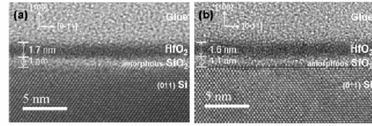
equivalent oxide thickness. According to Fig. 1-1, we can see the thickness was changed with higher process temperature. The EOT were also derived as 2.6nm, 2.7nm for 430℃ and 550℃ samples, respectively. The EOT were been thicker seems refer to an interaction between the SiO2 and HfO2 films and it will degrade the
device performance. So these phenomena should be avoided [48].
1.3 Effects of post-deposition-annealing on HfO
2There are many researches about the PDA effects on HfO2. The structure
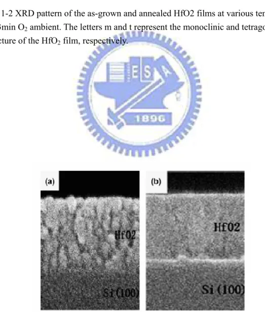
stability and quality depends on the film thickness and annealing temperature. Too high PDA temperature will make the HfO2 structure form a polycrystalline structure.
It will induce a very large leakage current and degrade the device performance. In Fig. 1-2, XRD patterns demonstrate that the as-grown HfO2 films are amorphous and the structure of the annealed HfO2 films undergoes a transformation of tetragonal to
monoclinic phase with increasing annealing temperature and forms a ployscrstalline structure at high annealing temperature. In Fig. 1-3, after annealing at 800℃, the thickness demonstrates a slight reduction due to the film densification, which results from the further crystallization of nonstoichiometric film [49]. According to this references, we can expected the device performance will show as better as increasing annealing temperature, but not more better as a too high annealing temperature over 1000℃..
1.4 Organization of This Thesis
In this study, we use an advanced process of ultra-thin oxynitride as interfacial layer with gate dielectric instead of traditional thermal SION and systematically discuss the reliability issue on n pMOSFETs. And then, we divided it into for chapters.
In chapter 2, we introduce the process flow for fabricating n, pMOSFETs device with ultra-thin oxynitride and gate dielectric HfO2 stack. We will show the basic
electrical characteristics on this sample, split C-V to obtain mobility, charging pumping to verify the amount of interface states and carrier separation to gain leakage current mechanisms.
(CVS) and negative bias temperature stress (NBTS) on the devices.
In chapter 4, we summarize the results and important issues of this study. Some advise for future work are proposed.
Fig. 1-1 High resolution electron microscope images of HfO2/SiO2/Si stack deposited
Fig. 1-2 XRD pattern of the as-grown and annealed HfO2 films at various temperature for 3min O2 ambient. The letters m and t represent the monoclinic and tetragonal
structure of the HfO2 film, respectively.
Fig. 1-3 Cross-sectional SEM images of (a) the as-grown and (b) the HfO2 film annealed at 800℃.
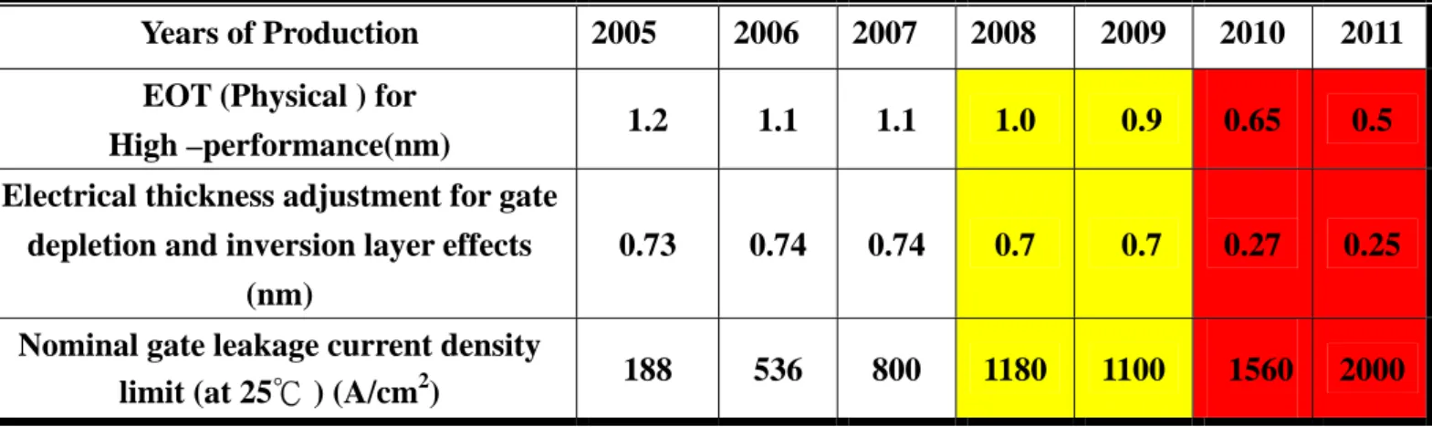
Table 1-1 2005 ITRS roadmap
Manufacturable solutions, and are being opitimized.
Manufacturable solutions are known.
Manufacturable solutions are not known.
Years of Production 2005 2006 2007 2008 2009 2010 2011 EOT (Physical ) for
High –performance(nm) 1.2 1.1 1.1 1.0 0.9 0.65 0.5 Electrical thickness adjustment for gate
depletion and inversion layer effects (nm)
0.73 0.74 0.74 0.7 0.7 0.27 0.25 Nominal gate leakage current density
Chapter 2
Electrical Characteristics of nMOSFETs with
Oxynitride and HfO
2gate stack
2.1 Introduction
Scaling of CMOS devices is projected as shown in Table 1 to continue down to deep sub-100nm regime [13]. The gate stack (dielectrics-silicon interface, gate dielectrics and gate contact) is arguably the most critical part of the MOSFET. It is widely believed that oxide will be replaced by high K dielectrics when dielectrics thickness is 1.5nm or below due to excessive direct tunneling (DT) gate leakage [14]. Due to the exponential increase in leakage current when scaling down the gate oxide thickness of MOSFETs, there is an urgent need to replace SiO2-based dielectrics by alternative dielectrics with high dielectric constants. Although the requested decrease in gate leakage current can be relatively easily realized, as is shown on Fig. 2-1, other parameters such as drive current and mobility are more difficult to achieve [15].
In high-k dielectrics, we faced high defect density in the bulk of high-k gate dielectrics and interfacial states in the gate stack structure are major reasons for Vth instability and mobility degradation [16]. However, the most serious problem is how
to suppress the leakage current caused by the interface states and defect traps, and how to suppress this problem especially at high temperature process. Most of high-k materials will become crystallized during high thermal process, and it will induce an un-uniform leakage current. The reliability issues of high-k dielectrics are also related to the interfacial layer between gate dielectrics-silicon interfaces. A research shows that the reliability of ALD (Atomic Layer Deposition) HfSiON high K gate stacks is greatly enhanced with a properly engineered IL (Interfacial Layer) between the gate dielectrics and the silicon substrate. It reports that the HfSiON, while deposited on an
optimized plasma-based IL containing [N], exhibits strong resistance to the
bombardment from heavy pocket implant species, achieving significantly reduced leakage and excellent reliability characteristics, compared to the HfSiON without an optimized IL [17].
In this thesis, we apply an advanced process about ultra-thin oxynitride to the MOSFETs technology. The proposed approach is realized by NH3 nitridation of
chemical oxide. As mentioned above, the performance of the device is related to the interfacial layer. On possible approach to form nitride oxides was post-oxidation annealing, including ammonia (NH3), nitrous oxide (N2O) and nitric oxide (NO)
annealing. As mentioned above, the traditional interfacial layer is grown by thermal nitrous oxide. Unfortunately, they usually require specific tools or gas. It is desired to
have a simple way to obtain the film and retain its quality. Compared with that in the case of the new process (developed in this paper), both thin thickness and film quality can be obtained successfully with low thermal budget, i.e., no rapid thermal process (900℃). Meanwhile, chemical oxide as a starting oxide can provide a better controllability in film thickness [18]. Nowadays, lower process temperatures and thinner oxynitride films are preferred in ULSI technology.
In this chapter, we compared with electrical characteristics for n, pMOSFETs with different rapid thermal annealing (RTA) process. We found the sample with 600 ℃ rapid thermal annealing (RTA) temperatures has better performance compared to the other sample with 900℃ rapid thermal anneal (RTA) temperatures and shows low leakage current compared to traditional thermally interfacial layer process on n, pMOSFETs. It shows the higher rapid thermal anneal (RTA) temperatures will contribute more degradation on the devices and better interfacial bonding with NH3
nitridation of chemical oxide than traditional interfacial layer.
2.2 Experiment
2.2-1 Experiment procedure
Standard local oxidation of silicon (LOCOS) process was applied for devices isolation. The n, pMOSFETs were fabricated on 6-inch p-type (100) Silicon wafers
utilizing conventional self-align process. After dipping sacrificial oxide about seven minutes by DHF, standard RCA clean was used to remove organic, particle and metal contamination. At once, the gate stack growth included three process steps, the first two steps were used to growth oxynitride as a interfacial layer-chemical oxide growth, and nitridation with NH3 purge. First step, the wafers were immediately
immersed into H2O2 solution at room temperature for 20 min to grow 10-Å-thick
chemical oxide. Second step, the chemical oxide was nitrided by low pressure chemical vapor deposition (LPCVD) furnace in low-pressure (120mTorr) NH3
ambient at 700℃ for 30 min. Third step, the nitrided chemical oxide was then sent to metal-oxide chemical vapor deposition (MOCVD) to deposit high-k gate dielectric HfO2. The ultra-thin oxynitride as an interfacial layer was growth in order to avoid
negative oxide growing before depositing high-k dielectric and decrease leakage current. The ultra-thin oxynitride was about 0.7nm~1.1nm and the HfO2 film was
about 30nm following by RTA at 600℃ and 900℃ in O2 ambient and then annealing
at 600℃ in N2 ambient to improve the quality of high-k dielectrics. A 200nm
poly-silicon was deposited by low pressure chemical vapor deposition (LPCVD). Subsequently, gate electrode was defined by I-line lithography stepper and etched by ECR etching system. After removing sidewall polymer, S/D extension implantation was implemented by Arsenic for nMOSFETs and Boron for pMOSFETs. Spacer
formation was carried out by plasma-enhance chemical vapor deposition (PEVCVD) and then the S/D implantation were executed by Arsenic for nMOSFETs and Boron for pMOSFETs. To continue patterning and S/D implant. Then, rapid thermal anneal (RTA) was performed at 950°C for 20 sec in N2 ambient to activate dopants.
Afterwards, SiO2 capping layer (5000A) was deposited by plasma-enhanced CVD
(PECVD) and contact hole patterning. And Al-Si-Cu metallization were implemented by PVD system and the patterning. After metal etching, forming gas annealing at 400 for 30minutes in N℃ 2/H2 ambient was used to fix dangling bond and reduce
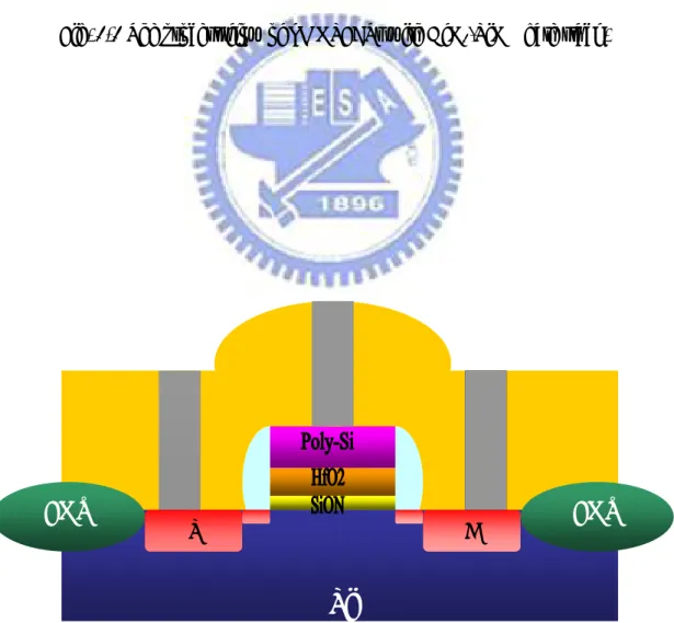
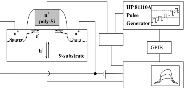
interfacial state density, Fig.2-2 shows the experimental flow, and Fig.2-3 shows the nMOSFET structure.
2.2-2 Measurement setup
Basic electrical characteristic such as I-V and C-V were measured by a HP4156A precision semiconductor parameter analyzer and HP4284 LCR meter, respectively. The equivalent oxide thickness (EOT) was obtained from high frequency (100 KHz) capacitance-voltage (C-V) curve at strong inversion without considering quantum effect.
Besides, the interface trap density (Nit) conversion was analyzed from charge
electrode, and the base voltage was varied from inversion to accumulation, while source/drain and body were grounded. The time varying gate voltage was fixed at pulse amplitude 1.5V. From the equation
qAf
Nit = Icp whereas A, f and q are the area
of gate electrode, the frequency of pulse voltage and electron charge, interface state density (Nit) could be extracted. Fig2-4 shows the configuration of measurement setup
used in our charging pumping experiment.
The electron mobility for nMOSFETs was evaluated by split C-V method. We know that drain current is a combination drift and diffusion currents as follows:
n eff n DS D eff Wu Q V kT dQ I Wu L q dx = −
The effective mobility was measured at low drain voltage (about -50mv or -100mv) and then gave:
n d eff WQ L g = µ
Where the drain conductance gd was defined as
nt consta V DS D d GS V I g = ∂ ∂ =
Qn was directly measured from capacitance measurements. The capacitance meter was
connected between the gate and the source-drain connected together with the substrate grounded. Therefore, Qn was expressed as follows:
∫
∞ − = GS V g gc n C dV Qas: o s n b eff K Q Q E ε η + =
∫
= GS V Vfb g gb b C dV Q∫
∞ − = GS V g gc n C dV QWhere Qb and Qn were charge densities in depletion region and inversion layer,
respectively. The parameter η=1/2 was for electron mobility, and η=1/3 was for hole mobility. And subsequently universal mobility was accomplished by following equation: 1.69 1 638 ⎟⎟ ⎠ ⎞ ⎜⎜ ⎝ ⎛ + = area eff eff ε µ , 5 180 1 ( / 4.5 10 ) p eff eff u ε = + ×
Above all equations, we easily can extract all of the data what we need. Fig 2-5 is the configuration of split-CV measurement setup.
2.3 Results and Discussion
2.3-1 Electrical characteristics of nMOSFETs with different
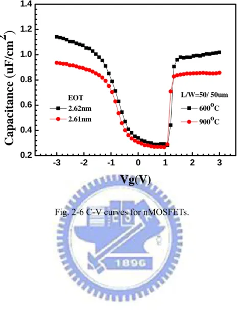
The C-V curves in Fig. 2-6 indicate not obvious change of EOT with different RTA temperature, this means the thickness of high-K dielectric HfO2 was not changed
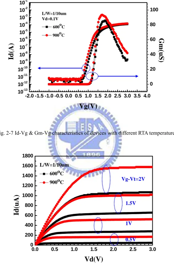
by post deposition anneal process. In Fig. 2-7 and Fig. 2-8 we also observe both drain current and transconductance have an apparent increase on the 900 ℃ RTA temperature sample. Fig. 2-9 and Fig. 2-10 depict the results of driving current and maximum transconductance versus different channel length. When channel length becomes shorter, the increase is more apparent.
Fig. 2-11 and Fig. 2-12 show the maximum transconductance versus various channel width and area. We can see that the 900℃ RTA temperature sample has obvious increase on maximum transconductance no matter in different channel length, width and area. The driving current and transconductance of 900℃ RTA temperature sample are higher than 600℃ RTA temperature sample. This is because the better densification in 900℃ RTA temperature sample we get. By the way, we can extract the interfacial trap density by charge pumping method. Fig. 2-13, Fig. 2-14 show the charge pumping current Icp for device with 600℃ and 900℃ RTA temperature, and
Fig.2-15 shows the comparison of charge pumping current Icp between the devices
with different RTA temperature. And then we can extract the value of Nit by equation
(2-1). Then we get Nit valuesof 1.818x1012cm-2 and 1.197x1012 cm-2 with 600℃ and
Fig. 2-16 shows that mobility versus effective electric field, we find the higher mobility we get in 900℃ sample. This is also caused by the better performance of higher high-K RTA temperature for the device. But using split-CV method wouldn’t calculate short channel device because the capacitance is too small and disturbance is too large, then we can’t get it by HP4284 LCR meter. Therefore, we only can measure the large dimensional device.
2.3-2 Conduction mechanism of nMOSFETs with Oxynitride and
HfO
2gate stack
The carrier type involved in the leakage current through HfO2/SiON dielectric
layers have also been investigated for unstressed nMOSFETs, using carrier separation method [19]. The contributing carrier of the gate leakage current can be separated into holes and electrons. Fig. 2-17 shows carrier separation results under the inversion region, and Fig. 2-18 shows carrier separation results under the accumulation region for N+-gated nMOSFETs with HfO2/SiON gate stack, both with 600℃ and 900℃
RTA temperature. It is found that the source/drain current ISD dominates the leakage
current under inversion region, and the substrate current IB dominates the leakage
under accumulation region. This indicates electrons from S/D that tunnel through gate dielectric is the dominant component of conduction mechanism under inversion
region , while holes from gate electrode that tunnel through gate dielectric is the dominant component of conduction mechanism under accumulation region.
This could be explained by band-diagrams shown in Fig. 2-19(a) and carrier separation experiment shown in Fig. 2-19(b). The substrate current IB corresponds to
the hole current from the gate , while the source/drain current ISD corresponds to the
electron current from Si substrate under inversion region. Hole supply from the gate conduction band in nMOSFETs is limited by the generation rate of minority holes in n+ gate. In other words, the probability of carriers from S/D that tunnel through gate
dielectric is strongly affected by tunneling distance and barrier height [20]. Because of the asymmetry of the HfO2/SiON band structure, it is more difficult for holes from
gate to tunnel through gate dielectrics compared with electrons from the channel. In nMOSFETs, electron current from the channel is the predominant injection current under stressing. The leakage component under accumulation region can also be explained by band-diagrams shown in Fig. 2-20(a), and the current component flow in carrier separation experiment is shown in Fig. 2-20(b).
In Fig. 2-21 and Fig. 2-22 , the gate current Ig as a function of Vg for the
HfO2/SiON layer is measured from temperature up to 125℃, both under inversion region and accumulation region for two samples. We obtain the leakage current is temperature dependent that increases with increasing temperature. It implies that the
conduction mechanisms of current must be trap-related like schottcky emission, i.e., trap-assisted tunneling (TAT), Frenkel-poole emission, etc.
The gate leakage current for devices with HfO2/SiON gate stack is composed of
two types of current, i.e., hole current and electron current. To determine the conduction process in the HfO2/SiON dielectric, Frenkel-poole (F-P) plots are fitted
for hole current and electron current, respectively, for both samples. The current from Frenkel-poole emission is of the form:
2 exp( B) B q a V I V n k T Φ ∝ − 0 ( / exp( B ox ins ) ox B q qE J B E k T πε ε − Φ − = ∗ 0 / ln( ) ox ins B) ox ox B B q qE q J E E k T k T πε ε Φ = −
⇒ intercept gives the Barrier height ( B B
q k T
Φ
− )
where B is a constant in terms of the trapping density in the HfO2 film , ΦB is
the barrier height, Eox is the electric field in HfO2 film. ε0 is the free space
permittivity, εinsis HfO2 dielectric constant, kB is Boltzmann constant , and T is the
temperature measured in Kelvin.
As shown in Fig. 2-20 and Fig. 2-21, are both under inversion region and accumulation region, excellent linearity for each current characteristic has been observed for two samples. This tendency indicates that both samples exhibit the
Frenkel-Poole conduction mechanism for the gate leakage current. Both the electron and hole conduction mechanisms are the same, and the result agree well with the F-P conduction mechanism.
2-4 Summary
In this work, we show the initial electrical properties of the device with different high-k RTA temperature. We found the 900℃ sample has the perfect performance about the higher driving current, higher transconductance, and higher mobility compared to 600℃ sample. In C-V curve, the EOT is almost equivalent for both sample, it seems the EOT was not changed by a higher PDA temperature process. We use carrier separation to verify that devices with different high-K RTA temperature, we found gate leakage current is the same with both devices. And conduction mechanism is Frankel-Poole emission.
Table. 1 SIA’s NTRS Projections [13]
Tech. Generation (nm) 100 70 50
Min. VDD (V) (desktop) 1.2-0.9 0.9-0.6 0.6-0.5
µprocessor (Gate Length) 70nm 50nm 30nm
Tox equivalent (nm) 1.5-2 <1.5 <1.0
Nominal Ion @25℃ (µA/µm) (NMOS/PMOS)
600/280 600/280 600/280 Max. Ioff @25℃ for
sub-nominal device (nA/µm)
Fig. 2-1 Gate leakage current vs. EOT for high k gate stack with poly-Si and metal gates.
․ Standard LOCOS Isolation ․ RCA clean and HF-last dip
․ Chemical Oxide Growth : H2O2 for 20min
․ Nitridation in NH3 ambient (120mTorr and 700℃ for
30min)
․ MOCVD of 30 nm HfO2
․ PDA 600℃, 900℃ 30sec in O2 ambient
․ PDA 600℃ 30sec in N2 ambient
․ Poly-Si deposition 200nm and pattering ․ Spacer formation, S/D extension, S/D implant ․ Dopant activation : 950℃ , 30sec
․ Passivation layer : SiO2 500nm
․ Metallization : Al-Si-Cu 900nm ․ Forming gas sintering : 400℃ , 30min
Fig. 2-2 The process flow of nMOSFETs with HfO2/SiON gate stack.
Fig. 2-3 Schematic cross-section of nMOSFETs with HfO2/SiON gate stack.
Si
FOX
FOX
Fig. 2-4 Basic experimental set-up of charging pumping measurement for nMOSFETs.
S
HP
GPIB 9-substrate n+ Source n+ Drain n+ poly-Si e -h+ HP 81110A Pulse Generator(a)
(b)
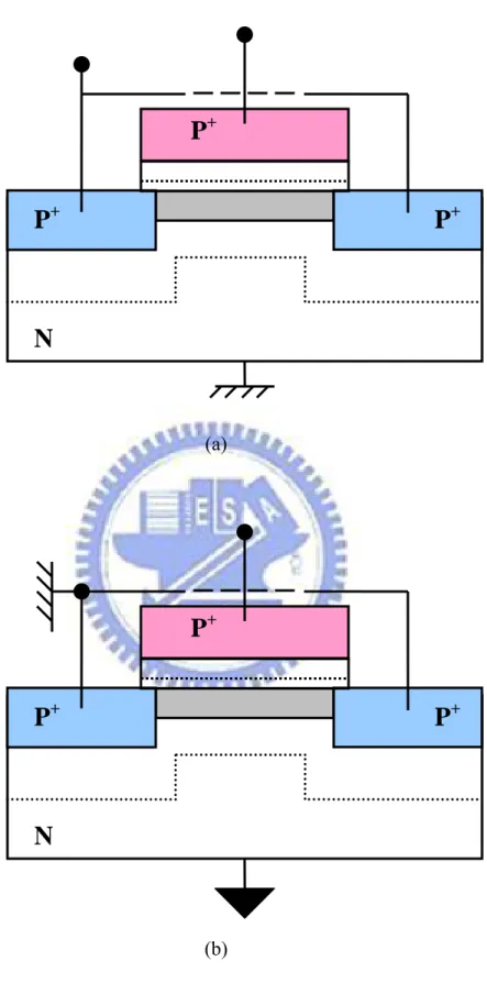
Fig. 2-5 Configuration for (a)gate-to-channel, and (b)gate-to-substrate capacitance measurement.
P
+P
+P
+N
P
+P
+P
+N
-3 -2 -1 0 1 2 3 0.2 0.4 0.6 0.8 1.0 1.2 1.4 EOT 2.62nm 2.61nm L/W=50/ 50um 600oC 900oC
Capacitance
(
uF/cm
2
)
Vg(V)
-2.0 -1.5 -1.0 -0.5 0.0 0.5 1.0 1.5 2.0 2.5 3.0 3.5 4.0 10-13 10-12 10-11 10-10 10-9 10-8 10-7 10-6 10-5 10-4 10-3 10-2 10-1 L/W=1/10um Vd=0.1V 600oC 900oC
Vg(V)
Id(A)
0 20 40 60 80 100Gm(uS)
Fig. 2-7 Id-Vg & Gm-Vg characteristics of devices with different RTA temperature.
0.0 0.5 1.0 1.5 2.0 2.5 3.0 0 200 400 600 800 1000 1200 1400 1600 1800 L/W=1/10um 600oC 900oC
Id(uA)
Vd(V)
Fig. 2-8 Id-Vd characteristics fro devices with different RTA temperature.
0.5V 1V 1.5V Vg-Vt=2V
0.4 0.6 0.8 1.0 1.2 1.4 1.6 1.8 2.0 2.2 0.60 0.65 0.70 0.75 0.80 0.85 0.90 0.95 1.00 1.05 1.10 Width=10um 600oC 900oC
Ab
s-Id
(
10
-4
A
)
@V
g
-V
t=1
V
Channel Length (um)
Fig. 2-9 Compared Idlinear with channel length for device with different
RTA temperature. 0.4 0.6 0.8 1.0 1.2 1.4 1.6 1.8 2.0 2.2 75 80 85 90 95 100 105 110 115 120 125 130 135 Width=10um 600oC 900oC
Gm
max
(us)
Channel Length (um)
Fig. 2-10 Compared Gmmax with different channel length for device with different
0 2 4 6 8 10 0 10 20 30 40 50 60 70 80 90
Gm
max
(us)
Channel Width (um)
Length=2um
600oC
900oC
Fig. 2-11 Compared Gmmax with channel width for device with different RTA temperature. 0.5X10 1X10 2X2 2X10 10X10 50X50100X100 0 20 40 60 80 100 120 140
Gm
max
(us)
Area
(
um2
)
Area=LxW 600oC 900oCFig. 2-12 Compared Gmmax with area for device with different
0.0 0.5 1.0 1.5 2.0 2.5 3.0 0 1 2 3 4 5 6
Icp
(uA)
Peak Voltage(V)
600oC sample Fixed Amp=1.5V L/W=50/50umFig. 2-13 Charge pumping current for device with 600℃ RTA temperature sample.
0.0 0.5 1.0 1.5 2.0 2.5 3.0 0 1 2 3 4 5
Icp
(uA)
Peak Voltage(V)
900oC sample Fix Amp=1.5V L/W=50/50um0.0 0.5 1.0 1.5 2.0 2.5 3.0 0 1 2 3 4 5 6
Icp(uA)
Peak Voltage(V)
600oC sample 900oC sampleFig. 2-15 Compared charge pumping current for device with different RTA temperature. 0.0 0.1 0.2 0.3 0.4 0.5 0 100 200 300 400 500
Mo
bi
li
ty
(
cm
2
/V
-S
)
Effective Field (MV/cm)
600oC 900oC UniversalFig. 2-16 Compared electron mobility with effective field for device with different RTA temperature.
0 2 4 6 8 10-10 10-8 10-6 10-4 10-2 IB W/L=20/20um IG=ISD 600oC IG 600oC ISD 600oC IB
Cur
re
n
t(A)
Vg(V)
(a) -8 -7 -6 -5 -4 -3 -2 -1 0 10-10 10-8 10-6 10-4 10-2 ISD IG=IBCur
re
n
t(A)
Vg(V)
600oC IG 600oC IB 600oC ISD W/L=20/20um (b)Fig. 2-17 Carrier separations with 600℃ RTA temperature sample under (a) inversion (b) accumulation region.
0 1 2 3 4 5 6 7 8 10-13 10-12 10-11 10-10 10-9 10-8 10-7 10-6 10-5 10-4 10-3 10-2 IB IG=ISD
Cur
re
n
t(A)
Vg(V)
900oC IG 900oC ISD 900oC IB W/L=20/20um (a) -8 -7 -6 -5 -4 -3 -2 -1 0 10-11 10-10 10-9 10-8 10-7 10-6 10-5 10-4 10-3 10-2 ISD IG=IBCu
rrent
(A
)
Vg(V)
900oC IG 900oC IB 900oC ISD W/L=20/20um (b)Fig. 2-18 Carrier separations with 900℃ RTA temperature sample under (a) inversion (b) accumulation region.
(a)
(b)
Fig. 2-19 n+-gated nMOSFET with HfO2/SiON gate stack under inversion region (a) band diagrams, and (b) Schematic illustration of carrier separation
experiment.
NMOSFET
n
+Gate
HfO
2e
-I
SD(-)
h
+ I B(-)P-Sub
Interfacial layer
n
+n
+n
+Vg(-)
Hole
injection
Electron
current
Electron
injection
(+)I
SD(+)I
BP
Inversion layer(a)
(b)
Fig. 2-20 n+ -gated nMOSFET with HfO2/SiON gate stack under accumulation region
(a)band diagrams , and (b)Schematic illustration of carrier separation experiment.
NMOSFET
n
+Gate
HfO
2e
- ISD(+)h
+ I B(+)p-Sub
Interfacial layer
n
+n
+n
+Vg(+)
Hole
injection
Electron
current
Electron
injection
(-)I
SD(-)I
BP
Inversion layer0 1 2 3 4 5 6 7 8 10-15 10-14 10-13 10-12 10-11 10-10 10-9 10-8 10-7 10-6 10-5 10-4 10-3 10-2 10-1 100
I g
(A)
Vg
25oC 75oC 100oC 125oC L/W=20/20um (a) -8 -7 -6 -5 -4 -3 -2 -1 0 10-15 10-14 10-13 10-12 10-11 10-10 10-9 10-8 10-7 10-6 10-5 10-4 10-3 10-2 10-1 100I g
(A)
Vg
25oC 75oC 100oC 125oC L/W=20/20um (b)Fig. 2-21 Gate leakage current versus gate bias for device with 600℃ RTA temperature.
0 1 2 3 4 5 6 7 8 10-15 10-14 10-13 10-12 10-11 10-10 10-9 10-8 10-7 10-6 10-5 10-4 10-3 10-2 10-1 100
I g
(A)
Vg
25oC 75oC 100oC 125oC L/W=20/20um (a) -8 -7 -6 -5 -4 -3 -2 -1 0 10-15 10-14 10-13 10-12 10-11 10-10 10-9 10-8 10-7 10-6 10-5 10-4 10-3 10-2 10-1 100I g
(A)
Vg(V)
25oC 75oC 100oC 125oC L/W=20/20um (b)Fig. 2-22 Gate leakage current versus gate bias for device with 900℃ RTA temperature.
Chapter 3
Reliability characteristics of nMOSFETs with
Oxynitride and HfO
2gate stack
3.1 Introduction
One of the main constraints for scaling down MOSFET’s dimensions is the device instability. Degradation of MOSFET’s can be caused by hot carrier stressing [20] ~ [24], Fowler-Nordheim tunneling injection [25] ~ [29] and the bias temperature stressing (BTS) [30] ~ [38]. In this chapter, we discuss about the latter one. In CMOS technology, the BTI issue is a very important reliability issue. Although the BTI issue is one of the earliest identified reliability problems, it has received relatively less attention. However, recent experimental results [36] have shown that the BTI can still make a considerable contribution to the degradation of small size MOSFET’s. However, in early research, the NBTI issue on SiO2 dielectric caused more significant degradation than PBTI does. While the NBTI includes both interface state generation and positive charge formation in the gate oxide, the PBTI only exists in the form of donor-like interface state generation. These donor-like interface states are localized symmetrically near the source and drain junctions and are negligible in the middle of the channel [39].
will cause the threshold voltage shift with stressing time. This phenomenon in high-k dielectric films with metal gated transistors has been identified as one the critical reliability issues that must be solved to implement high-k based CMOS transistors [40]. Previous reports in the literature on metal gate HfO2 based MOSFETs [41] ~ [43]
have observed that nMOS devices show significantly higher threshold voltage (Vt)
instability as compared to pMOS devices. This is contrary to observations in conventional gate oxide films. In conventional gate oxides, nMOS under positive bias temperature instability (PBTI) stress shows little or no threshold voltage degradation and hence is not a reliability concern. However, pMOS under negative bias temperature instability (NBTI) stress posses a continued reliability problem as the gate oxide is scaled thinner. In this study of HfO2 based poly gate MOSFETs, PBTI is
the major issue that must be solved to meet the required reliability specifications.
3.2 Measurement setup
Constant voltage stress (CVS) is method to evaluate the reliability of devices as it causes threshold voltage to shift with electrical stressing. A constant voltage stress is applied to device gate from Vg=2V~3V, while source/drain and substrate are grounded.
We measured Id-Vg and charging pumping during stress intervals. Id-Vg measurements
measurements are used to obtain interface density generation. Moreover, the total trap density which consists of interface trap density and bulk trap density is calculated from threshold voltage shift before and after stress. It expresses as follows
/
total th G
N C V qA
∆ = ∆ and bulk trap density also can be calculated as follows
bulk total it
N N N
∆ = ∆ − ∆
Positive bias temperature instability (PBTI) is an important reliability issue as it causes the threshold voltage to shift with electrical stressing at elevated temperature. To evaluate device degradations due to the bias temperature stress (BT), the gate electrode of the device was subjected to stress condition with negative bias (3V) varying from 25℃ to 125℃, while the drain/source and substrate were all grounded. The detail process is the same as CVS process, except temperature variation. Fig. 3-1 shows the experimental framework of our measurements.
3.3 Reliability of device with different High-K RTA
temperature
3.3-1 CVS of devices with different High-K RTA temperature
Fig. 3-2 (a) and Fig. 3-2 (b) expresses Id-Vg characteristics before stress and
sample and 900℃ sample. This means that interface state generation plays no significant role, rather, charge trapping in the bulk dielectric is the primary mechanism leading to CVS issues in high-k dielectrics. Vth shift of the 600℃ sample
is found to be slightly larger.
The threshold voltage shift (ΔVth) is measured with respect to the Id-Vg
characteristics with different high-K RTA temperature are shown in Fig. 3-3 in linear scale. The threshold voltage shifts toward negative gate voltage (ΔVth > 0), thus
implying that net negative charges are trapped in the gate dielectric layer as devices is measured. It is clear that 900℃ sample always shows smaller ΔVth than the 600℃
sample under different stress voltages as shown.
To further gain insights into the degradation mechanism during voltage stressing, the interface state generation, ΔNit, is plotted as a function of the stress time in Fig
3-4 (a) 600℃ sample ,and (b) 900℃ sample ,respectively. We found that 900℃ sample has lower shift of ΔNit, there is an excellent reliability performance especially
under CVS=3V.
Fig. 3-5 shows the overall comparison between both sample under CVS measurement at 25℃. We can see the 900℃ sample shows the less threshold voltage shift and less interface trap density shift compared to 600℃ sample.
3.3-2 PBTI of devices with different High-K RTA temperature
Fig. 3-6(a) and (b) expresses Id-Vg characteristics before stress and after stress at
125℃. Compared Fig. 3-2 (a) and (b), we found that there is observable change in ΔVth at high temperature, compared to that at room temperature, indicating that ΔNit increases with increasing temperature. This phenomenon is consistent with our results as shown in Fig. 3-8.
Fig. 3-7 compared the PBT-Stress-time dependence of threshold voltage shift for HfO2/SiON gate stack device with different high-K RTA temperature. A significantly
smaller Vth shift is observed for the 900℃ sample under the BT stress, Vg=3V at
25℃ and 125℃. Such phenomena can be attributed to the better thermal stability of oxynitride interfacial layer under higher PDA temperature annealing. This indicates that the Vth degradation could be more severe for the devices under BT stress at high
temperature [44]. The exponential value is temperature dependent relative to bulk trap generation. Fig. 3-9 shows the overall comparison between both sample under PBTI measurement. We can see the 900℃ sample shows the less threshold voltage shift and less interface trap density shift under 75℃ compared to 600℃ sample.
We found Vth degradation during PBTI stressing is serious in 600℃ sample
than 900℃ sample. According to Wang Hsin Chih’ paper, we found that interface states are not the main reason of threshold voltage shift. This indicates that charge
trapping in bulk is the main reason of threshold voltage shift [45]. The research has pointed out that amount of bulk traps is one to two order higher than amount of interfacial traps [46].
3.4 Summary
In this work, we found the 900℃ sample has less degradation than 600℃ sample. From CVS measurement, the value of is ΔNit larger than traditional SiO2
dielectric, but we still have the stable ΔNit after stress 1000s. We found the higher
high-K RTA temperature makes a better performance to reduce ΔVth. And the
exponential value of ΔVth is voltage dependent. From PBTI measurement, the
exponential value of ΔVth is voltage and temperature dependent. As a result, we can
confirm that charge traps in the bulk of HfO2/SiON gate stack are related to the
instability about threshold voltage shift and interface state shift. We can expect a continuous distribution of charge trapping cross sections, instead of a discrete-value capture cross section, in HfO2 high-K film [47]. Our experimental also shows that electron trapping is dominant in DC stress.
Fig. 3-1 Basic measurement method for (a) CVS (constant voltage stress), and (b) PBTS (negative bias temperature stress).
n+ n+ n+ P G ID-VG & CP DC stress 10sec ….. Charge pumping: To evaluate △Nit ID-VG: To evaluate △Gm ID-VG & CP ID-VG & CP ID-VG & CP DC stress 5sec DC stress 1sec
CVS for gate electrode CVS = 2, 3V △Vth & △Nit n+ n+ n+ P G ID-VG & CP DC stress 10sec ….. Charge pumping: To evaluate △Nit ID-VG: To evaluate △Gm ID-VG & CP ID-VG & CP ID-VG & CP DC stress 5sec DC stress 1sec
CVS for gate electrode CVS = 3V
Change T
0.0 0.5 1.0 1.5 2.0 2.5 3.0 3.5 4.0 10-11 10-10 10-9 10-8 10-7 10-6 10-5 10-4 pre-stress stress 1000s T=25oC, Vg=3V
Id(A)
Vg(V)
(a) 0.0 0.5 1.0 1.5 2.0 2.5 3.0 3.5 4.0 10-11 10-10 10-9 10-8 10-7 10-6 10-5 10-4 pre-stress stress 1000s T=25oC, Vg=3VId(A)
Vg(V)
(b)Fig. 3-2 Id-Vg characteristics for n+-gated nMOSFETs before and after stress 1000s at
25℃ (a) 600℃ sample, and (b) 900℃ sample.
Vth
10-1 100 101 102 103 104 40 45 50 T=25oC 600oC sample Vg=2V Vg=3V
∆
Vth(m
V
)
Stress Time
(a) 10-1 100 101 102 103 104 10 20 30 40 Vg=2V Vg=3V T=25oC 900oC sample∆
V
th
(m
V)
Stress Time (s)
(b)Fig. 3-3 Threshold voltage shift as a function of stress time, stressed at 25℃, Vg=2~3V in linear scale (a) 600℃ sample, and (b) 900℃ sample.
10-1 100 101 102 103 104 109 1010 1011 1012 T=25oC 600oC sample Vg=2V Vg=3V
∆
N
it
(
cm
-2
)
Stress Time (s)
(a) 10-1 100 101 102 103 104 109 1010 1011 1012 T=25oC 900oC sample Vg=2V Vg=3V∆
N
it
(
cm
-2
)
Stress Time (s)
(b)Fig. 3-4 Interface trap density shift increase as a function of stress time (a) 600℃ sample, and (b) 900℃ sample.
1 10 100 1000 0 10 20 30 40 50 60 70 80 90 100 600oC-2V 600oC-3V 900oC-2V 900oC-3V
∆
V
th
(mV)
Stress Time (s)
(a) 0.1 1 10 100 1000 10000 109 1010 1011 1012600oC-2V
600oC-3V
900oC-2V
900oC-3V
∆
N
it
(
cm
-2
)
Stress Time (s)
(b)Fig. 3-5 Compared of CVS measurement for devices with different RTA temperature (a) threshold voltage shift (b) interface trap density shift as a function of stress time.
0.0 0.5 1.0 1.5 2.0 2.5 3.0 3.5 4.0 10-9 10-8 10-7 10-6 10-5 10-4 pre-stress stress 1000s T=125oC, Vg=3V
Id(A)
Vg(V)
(a) 0.0 0.5 1.0 1.5 2.0 2.5 3.0 3.5 4.0 10-9 10-8 10-7 10-6 10-5 10-4 pre-stress stress 1000s T=125oC, Vg=3VId(A)
Vg(V)
(b)Fig. 3-6 Id-Vg characteristics for n+-gated nMOSFETs before and after stress 1000s at
125℃ (a) 600℃ sample, and (b) 900℃ sample.
Vth
10-1 100 101 102 103 104 30 40 50 60 70 CVS=3V 600oC sample 25oC 75oC 125oC
∆
Vth(mV)
Stress Time (s)
(a) 101 102 103 104 20 30 40 50 60 70 CVS=3V 900oC sample 900oC sample 25oC 75oC 125oC∆
V
th
(m
V)
Stress Time (s)
V (b)Fig. 3-7 Threshold voltage shift as a function of stress time under BTS at different stress temperature, Vg=3V in linear scale (a) 600℃ sample, and (b) 900℃ sample.
10-1 100 101 102 103 104 109 1010 1011 1012 1013 CVS=3V 600oC sample 4.64E+11 25oC 75oC 125oC
∆
N
it(
cm
-2)
Stress Time (s)
(a) 10-1 100 101 102 103 104 1010 1011 1012 CVS=3V 900oC sample 25oC 75oC 125oC∆
N
it(
cm
-2)
Stress Time (s)
(b)Fig. 3-8 Interface trap density shift as a function of stress time under BTS at different stress temperature, Vg=3V (a) 600℃ sample, and (b) 900℃ sample.
0.1 1 10 100 1000 10000 0 10 20 30 40 50 60 70 80 90 100
600oC-25oC
600oC-75oC
600oC-125oC
900oC-25oC
900oC-75oC
900oC-125oC
∆Vth(mV)
Stress Time (s)
(a) 0.1 1 10 100 1000 10000 1E9 1E10 1E11 1E12600oC-25oC
600oC-75oC
600oC-125oC
900oC-25oC
900oC-75oC
900oC-125oC
∆N
it
(
cm
-2
)
Stress Time (s)
(b)Fig. 3-9 Compared of PBTI issues for device with different RTA temperature (a) threshold voltage shift (b) interface trap density shift as a function of stress time.
Chapter 4
Conclusion and Future Work
4.1 Conclusion
Oxynitrides with high nitrogen concentration distributed close to the surface were investigated. We propose an alternative approach for forming a high-nitrogen ultrathin oxynitride gate dielectric is demonstrated.
In this thesis, the effect of high-K RTA temperature on the HfO2 gate stack were investigated. Several important phenomena were observed and summarized as
follows:
First, we have investigated its basic electrical properties. According to the initial electrical properties of the devices indicated the higher high-K RTA temperature has the better performance. The gate leakage current is analyzed by the carrier separation measurement, and can be explained by the band structure of the gate stack. The source/drain current ISD that correspond to the electron current dominates the leakage
under inversion region, while the substrate current IB that indicated the hole current dominants the leakage current under accumulation region. All leakage current can be categorized by fitting to be of Frenkel-Poole type.
and HfO2 gate dielectric with 600℃ and 900℃ high-K RTA temperature. ΔVth is
primarily caused by the charge traps in the HfO2 dielectric, not by the interfacial
degradation. The higher high-K RTA temperature is effective in densifying the HfO2
gate dielectric and showed the better performance.
4.2 Future Work
There are many issues and measurement skills that we can’t discuss completely. We list some goals for future work as follows.
1. HRTEM is used to verify real thickness and estimate value of the dielectric constant for HfO2/SiON gate stack.
2. SIMS analysis is used to prove nitrogen exist on the surface close to the gate dielectric.
3. In actual CMOS circuit operation, AC gate bias with specific frequency and duty cycle is usually utilized. Therefore, AC stress with Dynamic AC stress application is more realistic and can provide additional insights into the trapping behavior.
4. Fast transient pulsed Id-Vg measurement is also used to evaluate charge-trapping phenomena precisely.
![HPSH [ 氧化數平衡反應式係數 ]](data:image/gif;base64,R0lGODlhAQABAIAAAP///wAAACH5BAEAAAAALAAAAAABAAEAAAICRAEAOw==)