國立交通大學
顯示科技研究所
碩士論文
Polymeric Electrophosphorescent Devices with
Low Turn-on Voltages and High Power Conversion
Efficiencies by Blending with Poly(ethylene glycol)
高能量效率與低操作電壓之高分子電激磷光元件
研究生:簡上傑
指導教授:陳方中 博士
高能量效率與低操作電壓之高分子電激磷光元件
Polymeric Electrophosphorescent Devices with Low Turn-on
Voltages and High Power Conversion Efficiencies by Blending
with Poly(ethylene glycol)
研 究 生:簡上傑 Student:Shang-Chieh Chien
指導教授:陳方中 博士 Advisor:Dr. Fang-Chung Chen
國 立 交 通 大 學
電機學院顯示科技研究所碩士班
碩 士 論 文
A Thesis
Submitted to Display Institute
College of Electrical and Computer Engineering
National Chiao Tung University
in partial Fulfillment of the Requirements
for the Degree of
Master
In
Display Institute
July 2007
Hsinchu, Taiwan, Republic of China
高能量效率與低操作電壓之高分子電激磷光元件
碩士研究生:簡上傑 指導教授:陳方中
國立交通大學顯示科技研究所碩士班
中文摘要
本論文探討以[ITO/PEDOT:PSS/PVK:PBD:Ir(mppy)3/陰極]為主要結構的有機綠 光磷光發光二極體,在主動層中加入聚乙二醇[poly(ethylene glycol)],並嘗試不同的 陰極材料以探討有機層和金屬間的作用與元件整體表現的影響,以改善磷光發光 二極體的操作電壓。在以鋁作為金屬陰極材料時,經過混入聚乙二醇於主動層中,元件發光效率(Efficiency: cd/A)可從原本將近 0.28 cd/A提升到 15.6 cd/A,更重要 的是整個元件的起始電壓從 10V降低到 5.6V。另外,在以LiF/Ca/Al為金屬陰極材 料時,經過加入聚乙二醇到元件主動層內,也可以使元件的起始電壓從 4V降低到 3V,同時元件效率維持原本標準元件之發光效率 23 cd/A,因此可以使整個元件 的能量發光效率(Power efficiency: lm/W)從 9 lm/W提升到 14 lm/W。最後我們也成 功地利用此方法改善其他發光顏色元件的特性。
Polymeric Electrophosphorescent Devices withLow
Turn-on Voltages and High Power Conversion Efficiencies
by Blending with Poly(ethylene glycol)
Student:Shang-Chieh Chien Advisor:Dr. Fang-Chung Chen
Department of Photonic and Display Institute
National Chiao Tung University
Abstract
By blending poly(ethylene glycol) (PEG) into the active layer of green electrosphosphorescent devices, the luminance efficiency of the device with Al cathode achieves to 16cd/A.. More importantly, the turn-on voltage was lower than that of the conventional device. In addition, the device performance of this kind device with the LiF/Ca/Al cathode architecture after blending of 10 wt.% PEG was also investigated. It is found that the driving voltage of the device was lower than the conventional device, while the luminance efficiency reminds high. Consequently, a higher power conversion efficiency (14 lm/W) than that of the control device (9 lm/w) has been achieved. Finally, this work also has demonstrated the similar idea is successful for other color triplet device.
誌 謝
首先,誠摯地感謝這兩年來我的碩士生活的指導教授陳方中博士,提供良好的研究 環境和設備並且在實驗上給我很多實驗的技巧和想法,使我能夠在有機發光二極體上的 研究上更加得心應手,除了研究方面以外,老師也在做人處事態度上教導我鼓勵我,讓 我在碩士兩年不單只是研究上的進步還有培養更好的做事情態度。 在兩年的碩士生涯,很感謝以前學長們的帶領和指導,感謝文奎、喬舜、祖榮、志 平學長的指導和照顧,特別感謝志平學長提供基板的切割,讓我在此研究可以更順利。 另外感謝在碩一時候指導我的王文生學長,讓我對整個實驗、手套箱和其他實驗儀器的 更深入的了解。 同時也感謝的是陪我度過兩年同窗的實驗室夥伴們,義凱、泰元、浩偉、志力、尹 婷、紓婷,感謝你們在這兩年的陪伴、關懷、體諒和實驗上的協助。感謝義凱在碩士兩 年帶給實驗室的歡樂時光和實驗,運動以及玩樂上的陪伴、泰元在軟體還有數學上的幫 助、浩偉和志力在實驗上給予的建議和討論、以及尹婷和紓婷對整個實驗室的細心照 顧。如今大家都畢業了,祝福大家能夠在未來的人生路途上找到屬於自己的成就。 也感謝實驗室的學弟們,煒棋、永軒、政豪、信展、呈祥、昱仁、太獅以及學妹曉 芬。在碩士生涯最有關鍵的第二年,有你們的幫忙讓我在實驗上可以更加順利,感謝你 們對整個實驗室整個大小事情的盡心盡力、實驗儀器上的維護還有耗材藥品的購買,你 們的加入讓整個實驗室的團隊更加團結並且讓整個實驗室充滿歡笑的氣息! 最後感謝我的父母,感謝父母對於我的鼓勵和關懷並且適時的給予我建議,讓我能 夠有機會推甄上顯示科技所並且在碩士兩年順利畢業。同時也感謝我的女朋友靜宜在我 碩士兩年的陪伴以及對碩士忙碌生活的容忍和體諒。兩年的碩士生活,真的要感謝的人 太多了,在此完成學業之際,謹以此文獻給我所感謝的人。謝謝您們!Contents
_____________________________________________________________________
Chapter 1: Introduction ...1
1-1 Preface ...1
1-2 OLEDs structure...3
1-3 The operation of OLEDs ...4
1-4 The limitation of singlet polymer polymer light emitting diode..5
1-5 phosphorescent Organic light emitting diodes ...7
1-6 the mechanism of harvesting triplet excitons...7
Chapter 2: Motivation and Objective...10
2-1 My motivation ...10
2-2 Past literature for lower turn-on voltage ...11
Chapter 3: The experimental process for PLED...15
3-1 ITO pattern ...15
3-2 Clean of ITO glass substrate ...15
3-3 The fabrication processes of polymer light-emitting diodes...16
Chapter 4 Literature Review ...21
Chapter 5 Experimental Results ...25
5-1 Device performance based on Al cathode ...25
5-2 Device performance based on Ca/Al cathode ...28
Chapter 6 Discussions- Mechanism of PEG in active layer...33
6-1 Photovoltaic measurement for mechanism ...33
6-2 XPS measurement for chemcical interaction ...36
6-3 Different Ir(mppy)3 for triplet device with PEG ...38
6-4 AFM morphology with/without PEG...40
Chapter 7 Red phosphorescent PLEDs ...43
7-1 Red triplet device performance with PEG effect ...43
7-2 Increasing Ir(pid)(acac) dopant concentration ...46
Chapter 8 Conclusion and Future work...50
List of Table
Table 2-1 The efficiency, driving voltage and power efficiency of the same OLEDs[12] with different Alkali-complex. ... 13 Table 4-1 Device performance of RGB PLEDs based on PF-NR2/Al, Ba/Al, Al, in the
device structure: ITO/PEDOT:PSS/EL/Cathode ... 22 Table 6-1 Voc and △V turn-on with PEG and without PEG ... 36 Table 6-2 Device performance of different Ir(mppy)3 concentration with and without
Figure captions:
Chapter 1:
Figure 1-1(a) Flexible display (b) Wide-viewing angle... 1 Figure 1-2 (a) White OLED (b) Inket-Jet printing technology ... 2 Figure 1-3. The device structure of OLED ... 4 Figure 1-4. Left: the energy diagram of a device.
Right: schematic representation of recombination of holes
and electrons in device connecting to an external voltage source. ... 5 Figure 1-5. The triplet state and singlet state from two the recombination of electrons ... 6
Chapter 2:
Figure 2-1. How to get 100% quantum internal efficiency by triplet dopant ... 11 Figure 2-2(a) the device performance of OLEDs with various cathodes... 12 Figure 2-2(b). The performance of the same OLEDs with the different alkali-halide materials.[14] ... 12
Chapter 3:
Figure 3-1. The process for ITO pattern. ... 15 Figure 3-3-1. The chemical structure of PEDOT:PSS...17 Figure 3-3-2. The chemical structure of 1,2-dicrobenzen. ... 17 Figure 3-3-3. The standard device structure and the materials used in this study....18 Figure 3-3-4. the device structure... 19
Chapter 4:
Figure 4-1. Current density- voltage and efficiency-current density
Figure 4-2. The performance of the three different kinds of device. ... 22 Figure 4-3. The EL spectra of MEH-PPV, P-PPV, and PFO devices
with PF-NR2/Al bilayer cathode and Ba/Al cathode. ... 23
Figure 4-4. The left plot is current-density voltage.
The right plot is device efficiency. ... 24 Figure 4-5. Left plot is I-L-V curves of Alq3-based devices with different kinds of
cathode. Right plot the efficiency of OLEDs... 24
Chapter 5:
Figure 5-1 (a) current density (mA/cm2)-operating voltage(Volts) (J-V)
(b) Brightness (cd/m2)-operating voltage(Volts) (B-V) of Green triplet device based on Al cathode. ... 26 Figure 5-2 (a) Luminous efficiency (cd/A) vs current density(mA/cm2)
(b) power efficiency (lm/W)-current density(mA/cm2). ... 27 Figure 5-3 EL spectra for Ir(mppy)3 with blending PEG and without that based
on Al cathode... 28 Figure 5-4 (a) Current density (mA/cm2) - operating voltage (b) Brightness(cd/m2) - operating voltage of the PLEDs based on Ca/Al cathode. ... 29 Figure 5-5 (a) Luminous efficiency(cd/A) vs current density(mA/cm2)
(b) Power efficiency (lm/W) vs current density(mA/cm2). ... 30 Figure 5-6 (a) Current density(mA/cm2)- operating voltage (Volts)
(b) Brightness (cd/m2)- voltage (Volts) of PLEDs
based on LiF/Ca/Al... 31 Figure 5-7 (a) Luminous efficiency (Cd/A) vs current density(mA/cm2)
(b) Power efficiency (lm/W) vs current density (mA/cm2) ...32
Figure 6-1 The diagram of relation between Vbi and work function of cathode
and anode. ... 34
Figure 6-2 (a) (b) (c) Photovoltaic measurement on various cathode materials (Al , Ca/Al , LiF/Ca/Al). ... 35
Figure 6-3(a) XPS measurement (C spectra) on polymer with and without PEG based on Al cathode. ... 37
Figure 6-3(b) XPS measurement (C spectra) on polymer with and without PEG based on LiF/Al cathode ... 37
Figure 6-4 (a) the J-V curve and (b) the B-V curve of the different Ir(mppy)3...39
Figure 6-5 Current efficiency – operating voltage curve. ... 40
Figure 6-6 (a) and (b) the morphology of polymer film with / without PEG... 41
Figure 6-7 (a) and (b) the morphology of polymer film with / without PEG after deposition Al...42
Chapter 7:
Figure 7-1 The left picture is the chemical structure of Ir(pid)(acac). The right plot is the absorption and photo luminescent spectra of Ir(piq). ... 43Figure 7-2 (a) Current density (mA/cm2) - operating voltage (b) Brightness (cd/m2) – operating voltage of the red PLEDs based on Ca/Al cathode. ...44
Figure 7-3 (a) Efficiency (cd/A) – current density (mA/cm2) and (b) EL spectra of the device with and without PEG under the certain current density (c) EL spectra of the device with PEG under the different current density ...45 Figure 7-4 (a) Current density (mA/cm2) - operating voltage
based on Ca/Al cathode...47 Figure 7-5 (a)Efficiency (cd/A) – current density (mA/cm2)
(b) Power efficiency(lm/W)- current density (mA/cm2) of the red PLEDs
based on Ca/Al cathode. ...48 Figure 7-6 The EL spectra of red triplet device with PEG based on different dopant
Chapter 1
_________________ Introduction
1-1
Preface
“Organic light emitting diode” open the future of thin film full color displays with higher contrast, wide-viewing angle [Figure 1-1(b)], faster response, and low fabrication with easier processes. Most importantly, flexible display is our final achievement, therefore we have to do our best to make more and more researches on OLED/PLED [Figure 1-1(a)].
Figure 1-1(a) Flexible display (b) Wide-viewing angle
(www.universaldisplay.com) (www.opto.com.tw)
Polymer light emitting diodes (PLEDs) have attracted much interest worldwide since their discovery by R. H. Friend and co-workers in 1990[1]. Intense research is currently directed towards polymer light-emitting diodes (PLEDs) because of their potential for applications in the area of flat-panel displays. PLEDs are easily to be fabricated by spin-coating, ink-jet printing, or screen-printing technologies [Figure 1-2(b)].
Another application of PLEDs is light source, such as backlights in LCD (liquid-crystal displays), automotive dome lights and even illumination sources. Ideally, a white OLED should have excellent properties of low driving voltage, high efficiency, light weight, bright emission, CIE chromaticity coordinates of (0.33, 0.33) and high color render index. [Figure 1-2(a)]
Figure 1-2 (a). White OLED (b) Inket-Jet printing technology
(http://www.ubergizmo.com/)
1-2
Overview
Organic materials have became popular for many years. In our daily, there are so many things around us made of organic materials, for example, clothes, vehicles, and furniture. However we have not knew that organic or polymer materials have the ability to be conducting electrically until recently. In 1977, one important research about enhanced-conductivity of poly(acetylene) (PA) by chemical doping[2] was discovered. Since then, organic materials are not considered as only insulators but also conductors and semiconductors. Organic electronics have been the focus on the field of physics and chemistry for about 30 years.
In the past research, we know that we can change the electrical, physical and chemical properties of organic materials by modifying the chemical structures. Because of this property, organic materials have the great potential for the next generation electronics than inorganic materials. Many promising electronic devices made of organic materials, such as organic light emitting diodes (OLEDs) [3], polymer light emitting diode (PLEDs) [1], organic thin film transistor (OTFT) [4,5,6], organic photovoltaic devices [7,8],organic memory devices [9] and organic laser[10] have been fabricated nowadays. Because they have some advantages that inorganic electronic devices do not have, such as lightweight, flexibility, low cost fabrication process ability and easy process. Among all of the electronic devices, OLEDs have received the most attention in display industry and academia. Because of their unique properties, such
as wide viewing angle, fast response time, light weight, lower power consumption, OLEDs seem to have bright outlook in the future. Many scientist and enterpriser consider OLEDs as the next generation of display instead of LCD. In this work, OLEDs would be our research topic.
1-3
OLEDs structure
As noted above, the most highly advanced organic devices are organic light emitting diodes (OLEDs). There are two kinds of OLEDs; one is organic light emitting diode, and another one is polymer light emitting diode. What is the difference between the two? The most different point is the different type of material used. We use small molecule materials for OLEDs, and use thermal evaporation to accomplish it. We can accomplish multin-layer structure to improve the characteristic of OLEDs. On the other hand, conjugated polymer materials are used for PLEDs, and we usually use solution processes such as, spin-coating, dip-coating and ink-jet printing to accomplish the device. Although there are still some problems in PLEDs about the stability of devices, PLEDs have easier processes compared to those of OLEDs. We can use ink-jet printing to fabricate large panel and full-color displays in the future without any expensive thermal evaporating equipments.
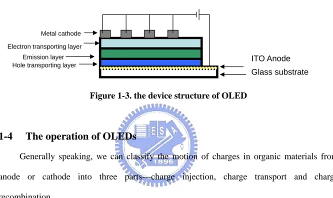
Common structure for organic light emitting diodes is like a sandwich (Figure 1-3) --- ITO Anode/Hole transporting layer/emission layer/electron transporting layer/Metal cathode. Because the emission light would be derived from the emission layer, a highly conductivity material with high transparent ability should be the anode of the device, such as ITO. On the other hand, suitable or metal cathode with low work-function compared with the LUMO of the organic material should be used. Because of that reason, we usually use low work function metal, such as Ca (Calcium), Cs (Cesium), or Ba (barium)[11] to be the cathode of OLEDs. However, the cathode metal with the low work function is so easy to be oxidized that the OLEDs have limited lifetime. Therefore, we usually use insulating materials such as, Li2O,
LiBO2, K2SiO3, LiF, CsF and Cs2CO3[12,13,14,15] with high work function metal such as, Ag
or Al instead of low work function. This kind electron injection metal can enhance the efficiency and lower operating-voltage of device, too. Electron and hole transporting layer which can improve electron-hole balance to enhance the luminous efficiency and internal quantum efficiency are the key issue for the performance of device; we can also choose the right emission layer depend on what kind of color we want.
Electron transporting layer
Glass substrate ITO Anode Hole transporting layer
Emission layer Metal cathode
Figure 1-3. the device structure of OLED
1-4
The operation of OLEDs
Generally speaking, we can classify the motion of charges in organic materials from anode or cathode into three parts---charge injection, charge transport and charge recombination.
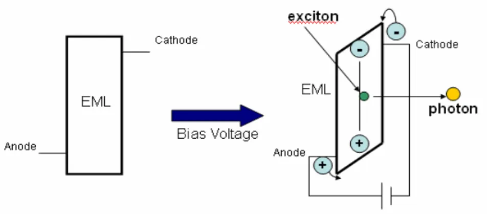
An OLED transform electrical energy into the excitation of organic molecule: electrons are injected from the cathode and holes from the anode. When we bias certain value of voltage on the device, there would be an electric field between the cathode and the anode. Under the influence of electric field, electrons and holes would hop toward the other side. Because of the coulomb interactions between such closely spaced carriers, a molecular excited state is not readily dissociated and its properties are conserved as it diffuses between molecules, allowing it to be treated as a particle. These states are known as “excitons”[1]. And then, the excitons would decay to ground state with the light emitting [Figure 1-4].
Figure 1-4. Left: the energy diagram of a device.
Right: schematic representation of recombination of holes and electrons in device connecting to an external voltage source.
So, the generation rate of “excitons” has been the most important factor on the quantum efficiency of OLED. The quantum efficiency of an OLED may be reduced if electrons or holes can leak all the way through the organic layers without recombination. The other reason is that the electron and hole have the different transporting motilities. There are many ways to solve such problem. An effective mean to prevent carrier leakage is to use multiple layers with different transport characteristics in organic hetrostructure. For example, the structure in Figure 1-3, some past papers showed the way to use the electron transporting layer to block the leakage of hole to the cathode, and the hole transporting layer to block the leakage of electron to the anode. This method would help the formation of excitons in the emission layer.
1-5
The limitation of singlet polymer light emitting diode
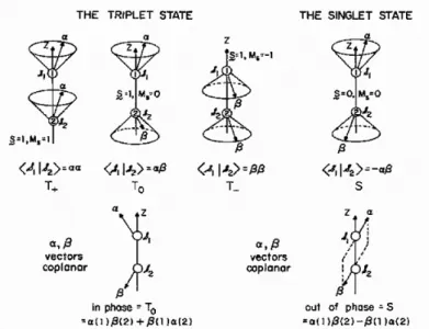
Since an exciton is formed from the recombination of a hole and an electron whose spin quantum number are both 1/2, we know that the exciton’s spin number is spin 0 or spin 1. According to simple quantum statistics, from Figure 1-5, the combination of two electrons’ spin direction results in four possible states. Spin 0 is singlet, written as |00>= 1 ( )
2 ↑↓ − ↑↓ . On the other hand, spin 1 is triplet, written as |11>= ↑↑,|01>= 1 (
2 ↑↓ + ↑↓) and |1-1>= , and triplet excitions have three possible states. In addition, we know the total spin number of the exciton in ground state is 0. Excitons with spin 0 can relax and release photons;
Excitons with spin 1 usually relax via other energy decay path without emitting of photons. The lifetime of singlet exciton is about several nano-second. On the other hand, for a triplet exciton, the relaxing process may take from several microseconds to a few seconds. Because of the reason mentioned above, from a typical polymeric light emitting diode, we cannot obtain the photon energy from triplet excitons relaxing from excited state to ground state. Therefore, the maximum internal quantum efficiency for a typical fluorescent (only singlet excitons work) polymeric light emitting diode is about 25%; there is 75% internal quantum efficiency would not be used in light emitting.[16]
Figure 1-5. The triplet state and singlet state from two the recombination of electrons.
1-5 Phosphorescent organic light emitting diodes
There were some researches about how to harvest triplet excitons in organic devices for enhancing the efficiency of polymeric light emitting diode in the past[17,18,19]. The first highly efficient electrophosphorescent device was reported in 1998 by M. A. Baldo et al.[18]. The doped electroluminescent devices has the more saturated red emission and higher external quantum efficiency (4%) and internal quantum efficiency (23%) than a typical fluorescent organic light emitting diode. Next chapter will explain how we can harvest triplet
excitons to at room temperature.
1-6
The mechanism of harvesting triplet excitons
The most efficient phosphorescent materials are organic complexes with heavy metal atoms, such as Pt, Ir, Os, Ru and Au. There is a high electron cloud density around the heavy metal atom, and the heavy metal atom can mix the triplet and singlet excition states. So a heavy metal atom can enhance the spin-orbital coupling process in organic compunds.
In the electrophosphorescent LEDs, the electrons and holes are injected into the organic host materials, and then the excitation is transferred to the organicmetallic emitters producing the phosphorescent excited states. This excitation energy transfer can occur by various mechanisms, including Förster and/or Dexter energy from the host material to the metal-organic center. On the other hand, direct sequential trapping of both electrons and holes on the metal-organic emitters can also play an important role. In the Förster energy transfer, the dipole-dipole interaction results in efficient transfer of the single excited-state energy from the host to the guest. Förster energy transfer from the host to the guest can lead to lower self-absorption losses because of the red-shift of the emission relative to the absorption in the blends. The rate (KFET) of Förster energy transfer is given by
1 6 0
( / )
FET d
K =τ− R R [20]
Where τ d is the lifetime of the host in the absence of the guest, R is the distance between the
host and guest, and R0 is the characteristic Förster radius which is given by
6 4 0 0 ( ) ( ) d a R α F ν ε ν ν dν ∞ − =
∫
[20]Where α depends on the relative orientation of the host and the guest dipole moments, the quantum yield of the host in the absence of the guest, and the refraction index of the medium;
and ( ) d
respectively. The efficiency of the Förster energy transfer depends on the spectral overlap between the host emission spectrum and the guest absorption spectrum. Generally speaking, the maximum distance over which Förster energy transfer can occur is 30~50A.[20]
Dexter energy transfer of a neutral exciton from the host to a neutral exciton on the guest requires direct quantum mechanical tunneling of electrons between the host and the guest. It is therefore a short-range process that requires short distant of no more than a few Å. In addition to singlet-singlet energy transfer, the Dexter mechanism also allows triplet-triplet energy transfer.
Forster and Dexter energy transfer can occur simultaneously when the energy of the singlet (or triplet) in the host is resonant with the corresponding levels in the guest. Although the conditions for Forster energy transfer can be easily evaluated from the absorption emission spectra, evaluation of the conditions for efficient Dexter transfer require knowledge of the absolute energies of the excited states. These energies are not available for most light emitting polymers.[21]
In the electron and hole trapping mechanism, an excited guest molecule is formed by the sequential trapping of a hole and then an electron onto the metal-organic complex. The hole- and electron- trapping mechanism is most favorable. While HOMO level of the guest is above that of the host, and the guest is below that of the host. However, having both the HOMO and LUMO of the guest within the gap of the host is not required. If the HOMO of the guest is above that of the host, holes will be readily trapped to form a cationic excited state of the guest. The cationic excited state of the guest will then function as an electron trap. Charge trapping and localization onto the guest requires overlap of the molecular orbital of the host and guest molecules. The use of Forster and/or dexter energy transfer from small molecules and semi conducting polymers as hosts to organnometallic emitters has been suggested for improving the external quantum efficiency of electrophophorescent OLEDs/PLEDs. The PL data that show very efficiency energy transfer, even at low concentrations of the organic-metal
emitter, argue against the importance of excitation transfer via the Dexter mechanism. Thus, the dominant mechanisms for PL and EL in polymers doped with organic-metal emitters are Forster energy transfer and charge trapping.[20,22]
Chapter 2
_________________ Objective and Motivation
2-1 Motivation
In recent years, polymer light emitting diodes (PLEDs) have demonstrated significant progress in electroluminescence (EL) efficiency and reliability, especially in the progress of triplet devices. Despite such progress, however, to survive the serious competition with other flat panel displays such as liquid crystal displays and plasma displays will require improved device characteristics. One of the most important research issues from the viewpoint of practical device applications is decreasing the driving voltage to improve power efficiency.
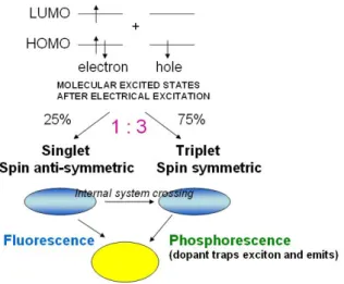
Intense research is currently directed towards polymer light-emitting diodes (PLEDs) because of their potential for applications in the area of flat-panel displays. PLEDs are easily to be fabricated by spin-coating, ink-jet printing, or screen-printing technologies. On the other hand, according to simple quantum statistics, 75% of excitons formed in the device are triplet[Figure 2-1.]. To harvest the triplet excitons, one effect way is to introduce phosphorescent dyes into the device. High device efficiency has been demonstrated following this concept. However, even through the quantum efficiency of triplet PLEDs can be enhanced by doping phosphorescent molecules, the charge trapping at the dopant sites usually cause the increase of operating voltage.
Figure 2-1. How to get 100% quantum internal efficiency by triplet dopant
In other words, the power efficiency, which is a more important and practical factor to evaluate the device, may not be improved as much as we expected.
2-2 Past literature for lower turn-on voltage and operating voltage.
1. The other metal materials with lower work function
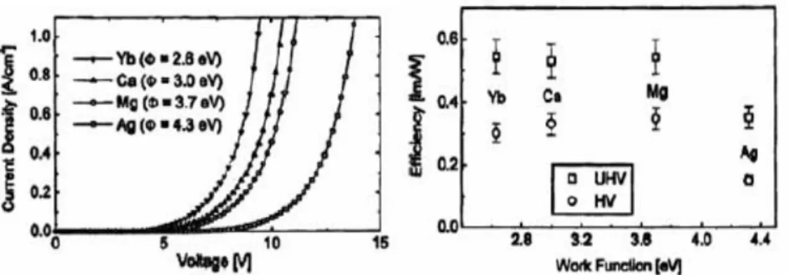
In order to lower the barrier height between active layer and cathode, low work function metals are commonly used to obtain high efficiency and lower operating voltage. In past literature, we can find many ways for decreasing turn-on voltage and operating voltage, such as finding a more suitable metal cathode with lower work function [Figure 2-2(a)][11]. But this way is not a good enough approach to obtain power efficiency; it just increases a little in power efficiency (lm/W). Meanwhile, low work function metals such as Ca, Ba are not stable in air and sensitive to water and oxygen. This kind of device must be stored in nitrogen-filled glovebox for achieving long operating time.
Figure 2-2(a) the device performance of OLEDs with various cathodes 2. Alkali-halide or Alkali-complex /Metal cathodes
Another solution for lower turn-on voltage is using some alkali complex as the electron injection layer between emission layer and cathode. For alkali-halide, the commonly used materials are CsF and LiF[14]; for alkali-complex, the commonly used materials are Li2O,
LiBO2, K2SiO3[12], and Cs2CO3[13] with the optimum thickness about 0.3nm-1.0nm. Devices
with the insulator materials between emission layer and air-stable metal can have lower turn-on voltage and higher efficiency. However, by this way, the thickness of the alkali-complex layer plays an important role in the performance of device, and one must find the optimum thickness of alkali-complex layer carefully for high efficiency OLEDs.
Figure 2-2(b). The performance of the same OLEDs with the different alkali-halide materials.[14]
Table 2-1 The efficiency, driving voltage and power efficiency of the same OLEDs[12] with different Alkali-complex
In addition to the two solutions for improving driving voltage, there are also some researches about inserting some organic hole transporting materials, electron transporting materials into the organic light emitting diodes between the anode and the cathode.
In this work, we would like to find one better and easy method to lower the turn-on voltage and increase the power efficiency without adding any other transporting layer or new metal cathode. We just need to dope one organic material in active layer, and only use some basic metal materials such as Ca/Al, Al to serve as the cathode. By blending poly(ethylene glycol) (PEG) into the emission layer of PLEDs, we can get the lower operating voltage and turn-on voltage. From the following equation for power efficiency (lm/W)-, a higher power
efficiency have been observed.
lm cd
W A V
π
= ×
(power efficiency=luminous efficiency
operating voltage π
×
− ) [35]
Chapter 3
__________The experimental process for PLED
3-1 ITO pattern
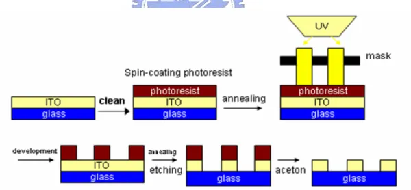
ITO (Indium Tin Oxide) is a kind of transparent conducting materials. Because its transparent property, ITO is always coated on glass substrate. So, we can use general optical lithography to get the ITO pattern. The process of optical lithography for ITO pattern is shown in Figure 3-1. First, we spin-coating photoresist on ITO glass substrate, and then we put shadow mask which we designed for ITO pattern on this glass substrate and let the glass substrate to be exposed to UV light for 100seconds. Next, the exposed parts of photoresist would be softer and removed in the process of development. After development, HCl was used to remove the ITO which is with no photoresist. Finally, the hard photoressistor is removed with aceton.
Figure 3-1. the process for ITO pattern
3-2 Clean of ITO glass substrate
After etching the ITO, the glass substrate should be completely cleaned. The process of cleaning ITO glass substrate is as following: washing ITO substrate with detergent, soaking in acetones soaking in propanel, flushing with DI water, and drying by a nitrogen gun. All of the
soaking process was done in an ultrasonic cleaner, which results in microvibrations to clean the surface. The process of cleaning of ITO glass substrate could play an important role in the device performance. The clean degree of ITO substrate would influence the efficiency of devices significantly. If the glass substrate is not clean, the uniformity of polymeric layer will be low.
3-3 The fabrication process of polymer light-emitting diodes
There are three parts for the fabrication processes of polymer light-emitting diodes:
1. Hole transporting layer: PEDOT:PSS[23]
Because of the chemical property of polymer, we can use some solution process such as spin-coating, ink-jet printing, and drop casting to fabricate the polymer light emitting diodes. The first layer to be deposited is hole transporting layer PEDOT:PSS
[Poly(3,4-ethylenedioxythiophene)-poly(styrene sulfonate)], which is a highly hole-transporting conducting polymer and is deposited from an aqueous suspension. Its work function is about 5.0 +/-0.2 eV, which matchs to the HOMO of the organic materials. For the process of coating PEDOT:PSS, because it is dissolved in water, ITO substratewas treated to be hydrophilic by exposure to an UV-Ozone for 15minutes. The function of UV Ozone is not only to increase the hydrophilic property of the ITO surface, but also decrease the work function to improve the injection of hole. On the other hand, ITO surface is always quite rough, and spin coating PEDOT:PSS on the ITO surface can both smooth the surface and stabilize the work function of the anode of the PLEDs. It is one of the keys to reproducible devices. Annealing at 120oC for one hour to remove the solvent is the final process of PEDOT:PSS. The chemical structure of PEDOT:PSS is shown in Figure 3-3-1.
Figure 3-3-1. the chemical structure of PEDOT:PSS
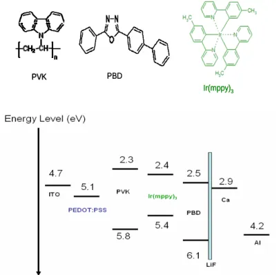
After a cleaned ITO glass substrate was firstly covered by about 70nm PEDOT:PSS, the next process is the coating of the active layer or the emission layer of the PLEDs. The most commonly material used was the blend of PVK,PBD, and Ir(mppy)3 with the ratio of PVK:PBD:Ir(mppy)3= 70:29:1[24] .
2. Light emissive layer
Blends of poly(vinylcarbazole)(PVK) [25]2-(4-Biphenylyl)-5-(4-tert-butyl-phenyl), -1,3,4-oxadiazole (PBD), and Ir(mppy)3[26] in 1,2-dicrobenzen (Figure 3-2-2.) solutions were
spin coated on the top of the PEDOT:PSS layer inside the glove box (N2 environment) and
then annealed at 80oC for 30mins. The device structure and the chemical structures of the materials used in this study are illustrated in Figure 3-3-4 and 3-3-3. The thickness of the emission layer is about 70nm (measured by AFM). Then, the samples were transferred into the thermal evaporator in a nitrogen atmosphere for metal deposition.[24]
Cl
Cl
1,2-dichlorobenzene
PVK PBD
Ir(mppy)3 PVK
PVK PBD
Ir(mppy)3
Figure 3-3-3. The standard device structure and the materials used in this study
3. Metal deposition
First, the substrates are put into a shadow mask which can define the area of active region (emission region). A Wu boat with a aluminum metal slab, a tungsten filaments with calcium and a crucible with insulating material. The environment is then pumped into high vacuum (about 5 × 10⁻⁶ torr) by mechanical pump and diffusion pump. Then the boat is heated up and the target material melts and evaporates, going straight from the boat to the substrate due to the high vacuum level. The rate of deposition can be adjusted to be optimum by controlling the current through the boat. The process is the same for any other material. On the other hand, there are some researches about the effects of the insulating layer such as Cs2CO3[27],
LiF[13], and CsF[28,29] between the emissive layer and the cathode metal. The past literatures show that the insulating layer can improve the injection of electron efficiently. So, in this work, LiF would be used to be one kind of cathode material.
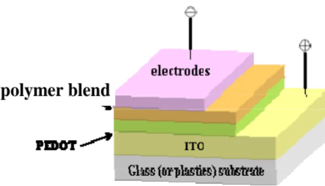
ITO/PEDOT:PSS/PVK:PBD:Ir(mppy)3/Al(100nm) (or Ca(50nm)/Al(100nm) ,
LiF(8A)/Ca(30nm)/Al(100nm)).[30,24]
polymer blend polymer blend
Figure 3-3-4. the device structure 4. Packaging and measurement of the devices
After thermal-evaporating the insulating layer and the cathode, we need to package devices with a piece of glass to avoid the organic and metal materials being exposure to water and oxygen. This process includes applying the limpid packaging adhesive on the device, covering glass on it, and exposing the sample to UV light for about 6minutes. Then, the packaging adhesive holds the two pieces of glass together.
Current density-voltage (J-V) and brightness-voltage (B-V) measurements are measured by using a Keithley 2400 power source measuring unit and a Keithley 2000 digital multimeter with a silicon photodiode in nitrogen-filled glovebox. The photocurrent value measured by photodiode will be calibrated by according to the real brightness value (cd/m2) which is obtained from PR650 SpectraScan Colorimeter measurement. The photovoltaic measurement was performed under the illumination supplied by a Thermo Oriel 150 W solar simulator (AM 1.5G). EL spectra of the devices are measured using the PR650 SpectraScan Colorimeter.
3-4 The experimental tools and measurement tools
1. Supersonic vibrate2. UV- Ozone 3. Spin-Coater
4. AFM (Atomic Force Microscope) 5. PL spectraometer
6. Current density-voltage and brightness measurement: Keithy 2000, Keithy 2400, Silicon diode (HAMAMATSU) with computerization Labview controller
7. Current density-voltage, brightness measurement, EL spectra and CIE index: PR650 and Keithy 2400 with computerization Labview controller.
8. Thermal Evaporator in Glovebox 9. Nitrogen-filled glovebox
Chapter 4
__________ Literature Review
In this chapter, some past papers about how to lower the turn-on voltage without changing metal cathode material or inserting other electron or hole transporting materials are reviewed. For example, “high efficiency low operating voltage polymer light emitting diodes with aluminum cathode” was reported by Y. Cao et al in 2004[31]. The performances of the PLED are shown in Figure 4-1. A standard singlet device for MEH-PPV blending with PEG based on Al cathode would have higher efficiency of that without PEG, but the paper have demonstrated this idea only useful Al cathode, not for Ca, Ba, Ag, and Au metal. Also, blending PEG to active layer can lower the turn-on voltage of MEH-PPV PLED.
Figure 4-1. Current density- voltage and efficiency-current density based on different cathode metal.
Yong Cao et al also reported one literature about another method to improve the device efficiency and turn-on voltage[32]. This paper have demonstrated that it also have the similar effect when they use bilayer cathode consisting of Al and alcohol-/water-soluble conjugated polymers such as PF-NR2 [poly[9,9-bis(3’-(N,N-dimethylamino)propyl)-2,7-fluorene)-
alt-2,7-(9,9-dioctylfluorene)] (X= I or Br). The standard device structure is ITO/PEDOT:PSS/MEH-PPV/Al, compared with this structure with PF-NR2 and that with low
work-function metal Ba. The results are shown in Figure 4-2.
Figure 4-2. The performance of the three different kinds of device.
Meanwhile, this work also apply the same idea to the PLEDs with the green color (P-PPV) and blue color (PFO). Table 4-1 is shown the results of the three different colors of PLEDs, and adding the PF-NR2 does not change the EL spectra[Figure 4-3].
Table 4-1. device performance of RGB PLEDs based on PF-NR2/Al, Ba/Al, Al, in the
Figure 4-3. The EL spectra of MEH-PPV, P-PPV, and PFO devices with PF-NR2/Al
bilayer cathode and Ba/Al cathode.
On the other hand, one literature is about using PEG which was fabricated by thermal coating to do the similar effect mentioned before[33]. “Organic oxide/Al composite cathode in efficient polymer light-emitting diodes.” was reported by T F. Guo et al in 2006. This paper is about the same idea under the different treatment and fabrication. The author thought although that the spin-coating is a conventional method for polymer materials, we cannot control the thickness of buffer layer easily to find the optimum condition for the best device performance. So, this paper develops a process for thermally evaporating an organic-oxide polymer layer with a low molecular weight poly (ethylene oxide), onto the surface of the emission layer film in a high vacuum before thermal coating Al cathode. The device structure is ITO/PEDOT:PSS/HY-PPV/PEGDE/Al, and PEGDE is controlled in 12Å, 25Å, 50Å, 75Å by thermal evaporating under 10-6 Torr. From results shown in Figure 4-4, in this way, the turn-on voltage and efficiency of device can be improved better to be than the control device. However, there are some problems about mixing between two polymer layers when we make multi-layer PLEDs and the optimum thickness of the layer, and we must treat these problems seriously.
Figure 4-4. The left plot is current-density voltage. The right plot is device efficiency.
Furthermore, T F. Guo et al. took advantage of the same idea to the small molecular organic light-emitting diodes based on Alq3 materials[34]. The results of this idea are shown
in Figure 4-5. The device structure is ITO/PEDOT:PSS/Alq3/PEGED/Al, and this work also
used thermal coating for PEGDE layer.
Figure 4-5. Left plot is I-L-V curves of Alq3-based devices with different kinds of
Chapter 5
__________ Experimental Results
Results about blending of PEG into the active layer of the green triplet device based on three kinds of metal cathode will be shown in this chapter.
The control device is definited as the one with the following device structure:
ITO/PEDOT:PSS/PVK:PBD:Ir(mppy)3/metal cathode
(Metal cathode: Al(100nm) , LiF(8A)/Ca(30nm)/Al(100nm) ).
The composition of the emission layer is [PVK:PBD:Ir(mppy)3 =70:29:1][24]. In addition, 10
wt.% PEG was added to investigate the effect of the inert dopant on the device performance.
5-1 Device performance based on Al cathode
First, we blend PEG into the active layer of polymer light-emitting diodes based on Al. The device structure is ITO/PEDOT:PSS/PVK:PBD:Ir(mppy)3(with or without PEG)/Al
(1000nm). Figure 5-1 (a) and (b) show the current density (J-V) and brightness-current density (B-J) curves of the PLEDs with and without 10 wt.% PEG in the emission layer, while the cathode used is Al. From the J-V curve, we can see the much larger current-density than the unblended device at the same voltage. In addition, the turn-on voltage (at 0.1 cd/m2) decreased from 10V to 5.6V; the degree of reducing turn-on voltage is about 4.4V. The significant change of the turn-on voltage reflects the improvement of charge-injection between the active layer and two anodes. From Figure 5-2(b), the device with PEG exhibits significantly higher output light for the device with PEG under the same bias. The luminance of the device with PEG exceeds 1600cd/m2, while the largest luminance of the control device is only 44.6cd/m2.
0 2 4 6 8 10 12 14 16 18 0 5 10 15 20 25 Curr ent density (mA/cm 2 ) V o ltag e (V ) C o n tro l d e v ic e d e v ic e w ith 1 0 w t.% P E G (a) 0 2 4 6 8 10 12 14 16 18 0 200 400 600 800 1000 1200 1400 1600 1800 C o n trol d ev ice d ev ice w ith 10 w t.% P E G Brig htn e s s (c d/ m 2 ) Voltage (V) (b)
Figure 5-1 (a) current density (mA/cm2)-operating voltage(Volts) (J-V)
(b) Brightness (cd/m2)-operating voltage(Volts) (B-V) of Green triplet device based on Al cathode
Figure 5-2(a) and (b) are the plot for the luminous efficiency (cd/A)-current density (mA/cm2) and the power efficiency (lm/W)-current density (mA/cm2). From Figure 5-1(c), the luminescence efficiency of the device with PEG (15.6cd/A) is much higher than that of the control device (0.28cd/A). Meanwhile, because of the reducing of turn-on voltage and enhancement of luminous efficiency, the power efficiency was increased from 0.12 lm/W to 5 lm/W. This is very important result for phosphorescence devices with Al cathode, because Al is an air-stable cathode for PLEDs and power efficiency is more important and critical for
lighting application of PLEDs being light source. Furthermore, we can achieve such high efficiency using Al cathode solely.
0 5 1 0 1 5 2 0 2 5 0 .1 1 1 0 C o n t r o l d e v ic e d e v ic e w ith 1 0 w t. % P E G E fficiency(cd/ A) C u r r e n t D e n s it y ( m A /c m2) ( a ) e n h a n c e f r o m 0 .2 8 c d / A to 1 5 .6 c d / A 0 5 1 0 1 5 2 0 2 5 1 2 3 4 5 P o w e r eff iciency ( lm /W) c u rre n t d e n s ity (m A /c m 2 ) C o n tro l d e v ic e D e v ic e w ith 1 0 w t.E G (b ) E n h a n c e fr o m 0 .1 2 lm /W to 5 lm /W
Figure 5-2 (a) Luminous efficiency (cd/A) vs current density(mA/cm2) (b) power efficiency (lm/W)-current density(mA/cm2).
Figure 5-3 compares EL spectra for the Ir(mppy)3 green triplet device with blending PEG and
without blending based on Al cathode. From Figure 5-1 (e), almost identical EL spectra were obtained for the two types of devices, so blending PEG does not result in any significant variation in EL spectra.
400 500 600 700 800 0.0 0.2 0.4 0.6 0.8 1.0 N
ormalized counts (a.u)
Wavelength (nm)
The Control Device The Device with PEG
λ max=508nm, Δλ= 68nm
Figure 5-3 EL spectra for Ir(mppy)3 with blending PEG and without that based on Al
cathode
5-2 Device performance based on on Ca/Al cathode
Next, we also make the same experimental condition with the other cathode to see if the effect still exists. And we find that there is the similar result for the PEG device with the Ca/Al cathode. Figure 5-4 (a) and (b) show the current density-voltage (J-V curve) properties and the brightness-voltage properties (B-V curve) of the devices with and without PEG using Ca/Al as the cathode architecture. From this two figures, it is clear that the device with 10 wt.% PEG has the similar change with Ca/Al cathode when we applied the same voltage. And also, we can find thatthe driving voltage for device with 10 wt.% PEG is lower by 1.2 volts, and the brightness was enhanced under the same biased voltage. In addition, the turn-on voltage decreases from 4.4V to 3.2V ( for 0.1 cd/m2 ).
0 2 4 6 8 10 12 14 0 10 20 30 40 50 60 70 Control device
Device with 10wt.% PEG
curren t de nsity (mA/cm2) Voltage (V) (a) (a) 0 2 4 6 8 10 12 0 1000 2000 3000 4000 Control device
Device with 10wt.% PEG
Bright ness( c d/m 2 ) Voltage (V) (b) (b)
Figure 5-4 (a) Current density (mA/cm2) - operating voltage (b) Brightness (cd/m2) - operating voltage of the PLEDs based on Ca/Al cathode.
From Figure 5-5 (a) and (b), we can see that the efficiency of PEG device still remains the same luminous efficiency (about 20 cd/A ) compared to the control device. Because of the same reason mentioned before, the device with lower driving voltage and the same luminous efficiency would have a higher power conversion efficiency (13.5 lm/w) [Figure 5-5 (a)] can be achieved. By this way, we have demonstrated that the power efficiency of triplet PLEDs with single active layer can be enhanced by blending PEG.
0.1 1 10 2 4 6 8 10 12 14 1 10 5 10 15 20 25 (lm/W) current density(mA/cm2)
enhance power efficiency from 9 lm/W to 13.5lm/W
Control device
Device with 10wt.% PEG
(C
d/A
)
(a)
(b)
remain the same efficiency about 20cd/A
Figure 5-5 (a) Luminous efficiency(cd/A) vs current density(mA/cm2) (b) Power efficiency (lm/W) vs current density(mA/cm2)
5-3 Device performance based on LiF/Ca/Al cathode
Finally, we also want to know what will happen if we insert an ultra thin layer of alkali metal fluorides between the Ca/Al cathode and the emissive layer. Because the PLEDs using LiF/Ca/Al have the higher efficiency and lower turn-voltage than that with Ca/Al, blending of PEG to the PLEDs based on LiF/Ca/Al may results in more significant effects. Therefore, we try the same condition for the device based on LiF/Ca/Al. Figure 5-6 (a) and (b) shows the current density-voltage properties (J-V curve) and the brightness-voltage characteristics (B-V curve) of the devices with and without PEG using LiF/Ca/Al as the cathode. From the figures, it is clear that the device with 10 wt.% PEG has much larger current density and brightness at the same bias, and the driving voltage for the device with 10 wt.% PEG is much lower. Similarly, the turn-on voltage ( at 0.1 cd/m2) also decreases from 4.2V to 3V, and the reducing degree of turn-on voltage is about 1V , which is the same with the performance based on Ca/Al mentioned on last section.
0 2 4 6 8 10 12 14 16 18 20 0 20 40 60 80 100 120 140 160 180 Cur re nt den s ity ( m A/cm 2 ) Voltage (V) control device Device with 10% PEG (a) 0 2 4 6 8 10 12 14 16 18 0 2000 4000 6000 8000 10000 control device Device with 10% PEG
Bri g h tn e ss(cd/ m 2 ) Voltage (V) (b)
Figure 5-6 (a) Current density(mA/cm2)- operating voltage (Volts) (b) Brightness (cd/m2)- voltage (Volts) of PLEDs based on LiF/Ca/Al
Besides, from Figure 5-7(a), we can see that the device efficiency of PEG device still remains 23 cd/A, which is compared to that of the control device. On the other hand, because of the lower driving voltage, higher power conversion efficiency (14 lm/w) can be achieved [Figure 5-7(b)]. All of the performances based on LiF/Ca/Al are similar as that using Ca/Al, so the PEG affects also occur while the cathode material is alkali-complex such as LiF. On the other hand, the EL spectra of the PLEDs with PEG and that without PEG are the similar as the control device no matter which metal cathode (Al, Ca/Al, LiF/Ca/Al) was used PLEDs based
on. 0 . 1 1 1 0 1 0 0 0 . 1 1 1 0 1 0 0 0 . 1 1 1 0 1 0 0 0 2 4 6 8 1 0 1 2 1 4 1 6 c o n t r o l d e v i c e D e v i c e w i t h 1 0 % P E G Efficiency(cd/A ) C u r r e n t d e n s i t y ( m A / c m 2 ) r e m a i n t h e s a m e e f f i c i e n c y = 2 3 c d / A 1 4 l m / W ( b ) power conv ersi on ef fi ci ency( lm/W ) C u r r e n t D e n s i t y ( m A / c m 2 ) ( a ) 9 l m / W t o
Figure 5-7 (a) Luminous efficiency (Cd/A) vs current density(mA/cm2) (b) Power efficiency (lm/W) vs current density (mA/cm2)
Chapter 6
Discussions-
_____________Mechanism of PEG in active layer
In last chapter, we have demonstrated one easy way to enhance the power efficiency and to lower the turn-on voltage by blending PEG into PLEDs. In this chapter, the mechanism will be discussed. The first measurement is photovoltaic measurement for the open circuit voltage (Voc) of the device with and without PEG under the different cathode materials. The change of the barrier height between the cathode and the polymer layer would be obtained from the difference of Voc. The second measurement is X-ray photoelectron spectroscopy (XPS) for the binding energy value. From XPS data, the interaction between the organic and metal interface would be investigated. Finally, trapping effect under the different dopant concentrations of the emission layer will be checked for PEG effect.
6-1 Photovoltaic measurement for mechanism
We can know the Voc (open-circuit voltage) value from photovoltaic measurement. Because the interface between these two electrodes and organic layer all are non-ohmic contact, Voc value is close to Vbi (built-in potential), which is the difference between the work
function of the anode and the cathode. Therefore, from Voc, we can understand if there are any change in the work-functions of the anode and the cathode. In more detail, from Figure 6-1, it is clear the built-in potential is the difference between the work function of the anode and the cathode. While the work-function of anode remains the same, we can know the change of the barrier-height between the polymer layer and the cathode from the change of the Voc value.
(Photovoltaic measurement condition:AM 1.5 ; 100mW/cm2)
Figure 6-1 The diagram of relation between Vbi and work function of cathode and anode.
Figure 6-2 (a) (b) (c) and Table 6-1 show the results of the photovoltaic measurement for the six devices, which are the devices with PEG and without PEG based on the three different kinds of cathode materials. The open-circuit voltage (Voc) of devices using the LiF/Ca/Al cathode is higher than that for Al cathode, expected from the lower work function and hence larger build-in potential. The same result from Ca/Al cathode was also observed compared with Al cathode. On the other hand, when PEG was blended into the emission layer, higher open-circuit voltages were obtained for all the devices. Consequently, it is speculated that adding PEG results in higher build-in potential, which can leads to lower turn-on voltage. Because of no substantial changes in the interface between PEDOT:PSS and active layer, the higher build-in potential implies reduced barrier height between the metal cathode and polymer blended with PEG.. This phenomenon is probably from some interaction between PEG and the cathode materials, leading to a lower barrier height of the electron injection. This kind of interaction can improve the balance of the electrons and holes and, hence, can also improve the device power efficiency.
0 .0 0 .5 1 .0 1 .5 1 0-5 1 0-4 1 0-3 1 0-2 Cur rent d ensity(mA/ c m 2 ) V o lta g e (V ) C o n tro l d e v ic e D e v ic e w ith 1 0 w t.% P E G C a th o d e : A l (a ) 0.0 0.5 1.0 1.5 1E-5 1E-4 1E-3 Control device
Device with 10 wt.% PEG
c u rr ent d ens ity( mA/c m2) Voltage(V)
Cathode
:Ca/Al
(b) 0.0 0.5 1.0 1.5 10-5 10-4 10-3 C u rr e n t de ns ity (m A /c m 2 ) Voltage (V) Control deviceDevice with 10 wt.% PEG
Cathod:LiF/Ca/Al
(c)
Figure 6-2 (a) (b) (c) Photovoltaic measurement on various cathode materials (Al , Ca/Al , LiF/Ca/Al).
Table 6-1 Voc and △V turn-on with PEG and without PEG
4-2 XPS measurement for chemical interaction between PEG and metal
cathode
From XPS measurement, we can know if there is any chemical interaction between PEG and metal cathode. From Figure 6-3(a), we can see that there is no change in C (carbon) spectra after adding of PEG for the polymer film without any metal deposition. On the other hand, we can see a little change in C spectra of XPS measurement for the polymer film with 3nm thick layer of thermally evaporated Al (3nm). Obviously, there is no chemical shift (remain the main peak 284.6eV (C-C) )after thermally evaporating Al metal on the film, but the intensity in the binding energy is enhanced after blending PEG. On the other hand, we can see that the C spectra (288eV~285eV) of the polymer film with PEG is broader than the polymer film without PEG based on Al cathode. In more details, from XPS data base [http://www.lasurface.com], the peaks at 283.5eV and 288.6eV correspond to the binding energy of (Al-C) and some Al2O3 alumina or (Al-O), so the intensity in 283.5eV and 288.6eV
would be increased after thermally evaporating Al metal on the film. In addition, 286.2eV~286.9 is the binding energy of (C-O) which increased in the polymer with PEG/Al sample and remain the same intensity in the other condition (pristine polymer, pristine polymer film with PEG and polymer/Al). From these results, PEG certainly creates some chemical interaction with Al, and the new binding or the new substance from that may provide a lower barrier height for the injection of electron.
cathode[Figure 6-3(b)]. We can speculate that there is some chemical interaction between PEG and metal. This kind of chemical interaction can result in lower barrier height between active layer/cathode and also enhance the injection of electron.
292 290 288 286 284 282 280 0.0 0.2 0.4 0.6 0.8
1.0 Pristine polymer Pristine polymer + PEG Polymer = PVK+PBD+Ir(mppy)3
Polymer /Al Polymer + PEG/Al Normali zed counts(a. u )
binding energy(eV)
288.6ev 284.6ev PO.+PEG/Al PO./Al 286.2eV 283.5evCathode:Al
(a)Figure 6-3(a) XPS measurement (C spectra) on polymer with and without PEG based on Al cathode 290 288 286 284 282 280 0.0 0.2 0.4 0.6 0.8 1.0 PO. Normali z ed count s (a. u ) Wavelength (nm) Polymer/LiF/Al Polymer+PEG/LiF/Al PO.+PEG 286.9eV 286.2eV
Cathode : LiF/Al
(b)Figure 6-3(b) XPS measurement (C spectra) on polymer with and without PEG based on LiF/Al cathode
6-3 Different Ir(mppy)
3for triplet device with PEG
Charge trapping effect play an important role in the turn-on voltage and operating voltage for phosphorescent device, so we are also curious about if blending PEG can make some effect on the charge trapping. Finally, we investigate this problems by adding different Ir(mppy)3 concentration to the triplets with PEG.
Figure 6-4 (a) (b) shows the current density- operating voltage curve (J-V curve) and the brightness-operating voltage curve of the different Ir(mppy)3 concentration for the device with
PEG and without PEG based on Ca/Al. From J-V curve, we can get the similar change when we blend PEG to the active layer no matter what percentage of Ir(mppy)3 is. It also remains
the same current efficiency after blending PEG to active layer in 1%, 3%, 6%, 11% Ir(mppy)3
concentration, and the turn-on voltage also decreases by the same degree (about 1V) [Table 6-1]. -2 0 2 4 6 8 10 12 14 16 18 0 10 20 30 40 50 60 70 Cur rent densi ty ( m A/ cm 2 ) Voltage (V) Ir 1% Ir 1% PEG Ir 3% Ir 3% PEG Ir 6% Ir 6% PEG Ir 11% Ir 11% PEG (a)
-2 0 2 4 6 8 10 12 14 16 18 -1000 0 1000 2000 3000 4000 5000 6000 7000 8000 9000 Br ightness (Cd/m 2 ) Voltage (V) Ir 1% Ir 1% with PEG Ir 3% Ir 3% with PEG Ir 6% Ir 6% with PEG Ir 11% Ir 11% with PEG (b)
Figure 6-4 (a) the J-V curve and (b) the B-V curve of the different Ir(mppy)3 concentration device with and without PEG based on Ca/Al cathode.
From Table 6-2, we can see that the luminous efficiency remain the same after blending PEG into the active layer for any concentration of Ir(mppy)3. And also, blending PEG into
active layer can decrease by the same degree. Therefore, the triplet devices with different dopant concentration all have higher power efficiency (lm/W) than that without PEG.. From the similar results based on different dopant concentration, we can know that the influence of PEG blending into active layer did not change when we change the Ir(mppy)3 concentrations.
Table 6-2 Device performance of different Ir(mppy)3 concentration with and without
PEG based on Ca/Al cathode
4.3V 3.5V 3.3V 3V Vturn-on (With PEG) 11.5 9.8 9.05 8.4 Peak of V 8.5 6.8 6.5 6.2 Peak of V (With PEG) 5.2V 4.88 5.8 15.6 17.6 11% 4.5 8.98 7.15 21.6 22.6 6% 4.2V 9.21 8.2 22.1 22.6 3% 4V 14.4 7.4 20.1 21.6 1% V turn-on Lm/W (With PEG) Lm/W Cd/A (With PEG) Cd/A Ir% 4.3V 3.5V 3.3V 3V Vturn-on (With PEG) 11.5 9.8 9.05 8.4 Peak of V 8.5 6.8 6.5 6.2 Peak of V (With PEG) 5.2V 4.88 5.8 15.6 17.6 11% 4.5 8.98 7.15 21.6 22.6 6% 4.2V 9.21 8.2 22.1 22.6 3% 4V 14.4 7.4 20.1 21.6 1% V turn-on Lm/W (With PEG) Lm/W
Ir% Cd/A Cd/A
(With PEG)
because of hole trapping in Ir(mppy)3 device, the higher Ir(mppy)3 concentration will lead to
more trapping, resulting in higher operating voltages. Because the more trapped holes in active layer, we need higher operating to let more electron inject to active layer for achieving charge balance (from Figure 6-5 (a) ). Then, from Figure 6-5 (b), we can see that the operating voltage of maximum current efficiency would be smaller after blending PEG into device, so blending PEG can improve the injection of electron and the charge balance under the smaller operating voltage. From this characteristic, it definitely shows that blending PEG to active layer can help the injection of electron.
2 4 6 8 10 12 14 0 5 10 15 20 25 2 4 6 8 10 12 14 0 5 10 15 20 25 Cd /A Voltage (V)
with PEG
without PEG
Ir(mppy)3 1% Cd/ A (b) (a) Ir(mppy)3 6%Figure 6-5 Current efficiency – operating voltage curve
6-4 AFM morphology with/without PEG
The interface between the polymer and the cathode plays an important role in determining the electrical properties of the devices and the morphology of the spun-coating polymer film need to be studied for the information of the metal-polymer interface. Because of the reason mentioned before, we also doubt that blending PEG into active layer may have some effect on the morphology or roughness of polymer film. In order to understand the morphological changes that occur in the polymer film after blending PEG, we use AFM (atomic force microscopy) to find out any difference between the film with and without PEG.
Figure 6-4 (a) and (b) are the polymer film without PEG and with PEG. The surface roughnesses of these two polymer films only almost the same; the surface morphology are also similar after blending PEG into active layer.
(a) Roughness:0.495nm (b) Roughness:0.478nm
The polymer film with PEG The polymer film without
Figure 6-6 (a) and (b) the morphology of polymer film with / without PEG
Although there is no change from Figure 6-6 (a) and (b), there are probably some changes happened after the deposition of metal cathode.
Therefore, we deposit Al metal on the polymer films with and without PEG, and then we removed the Al metal before AFM measurement. From Figure 6-7 (a) and (b), we can find out the polymer film without PEG has a higher roughness than that with PEG.. We can speculate one possible phenomenon after the deposition of Al metal on the polymer film with PEG, which may have the function that can suppress the diffusion of the metal atoms and blocks the doping reaction in the EL layer. That reaction would be less destruction on the polymer film when we deposit Al metal, which would quench luminescence. As a result, the triplet device with PEG based on Al has higher luminous efficiency than the polymer film without PEG.
r
(a) Roughness: 13.788nm (b) Roughness: 4.405nm
The polymer film without PEG The polymer film with PEG
Figure 6-7 (a) and (b) the morphology of polymer film with / without PEG afte deposition Al
Chapter 7
_____ __Red Phosphorescent PLEDs
__________
ea applies to the other color triple
[http://www ]
emical structure of Ir(pid)(acac). The right plot is the
rent density (J-V), brightness-current
7-1 Red triplet Device performance with PEG effect
Finally, we would like to know if it still works while this id
t dopants. In this work, we choose Red Ir dopant [Bis (1-phenylisoquinoline)- (acetylacetonate) iridium(III)] for our red triplet devices to investigate the mechanism. All of the process and device structure are the same with the process for green triplet devices as before. The device structure is ITO/PEDOT:PSS/PVK:PBD:Red Ir doapnt/Ca/Al. At first we tried the composition of the emission layer is [(PVK:PBD:Ir(piq)(acac) =70:29:3] with the solvent 1,2-Dicrobenzen. In addition, 10 wt.% PEG was added to investigate the effect of the inert dopant on the device performance.
.adsdyes.com/oled.htm
Figure 7-1 The left picture is the ch
absorption and photo luminescent spectra of Ir(piq)
Figure 7-2 (a), (b) and Figure 7-3 (a) show the cur
density (B-J) curves and efficiency-current density curves of the PLEDs with and without 10 wt.% PEG in the red emission layer, while the cathode used is Ca/Al. From Figure 7-2 (a) and (b), although the PEG effect also results in the lower turn-on voltage and higher current density under the same operating voltage, the brightness is not enhanced as we expected. Because of the lower brightness for PEG device, the red triplet device also has the lower
![Table 2-1 The efficiency, driving voltage and power efficiency of the same OLEDs[ 12 ] with different Alkali-complex](https://thumb-ap.123doks.com/thumbv2/9libinfo/8762041.208415/25.892.247.689.548.779/table-efficiency-driving-voltage-efficiency-different-alkali-complex.webp)