具有超薄高介電常數閘極介電層與應變矽鍺通道之先進深次微米金氧半場效電晶體研究
201
0
0
全文
(2) 具有超薄高介電常數閘極介電層與應變矽鍺通 道之先進深次微米金氧半場效電晶體研究 Advanced Deep Sub-Micron MOSFETs with Ultra-Thin High-k Gate Dielectrics and Strained SiGe Channel 研究生: 陳經緯 指導教授: 張俊彥 博士. Student: Ching-Wei Chen Advisor: Dr. Chun-Yen Chang. 國 立 交 通 大 學 電子工程學系 電子研究所 博 士 論 文 A Dissertation Submitted to Department of Electronics Engineering and Institute of Electronics College of Electrical Engineering and Computer Science National Chiao Tung University In Partial Fulfillment of the Requirements for the Degree of Doctor of Philosophy in Electronics Engineering July 2005 Hsinchu, Taiwan, Republic of China. 中 華 民 國 九 十 四 年 七 月.
(3) 具有超薄高介電常數閘極介電層與應變矽 鍺通道之先進深次微米金氧半場效電晶體 研究 研究生: 陳經緯. 指導教授: 張俊彥 博士. 國 立 交 通 大 學 電子工程學系 電子研究所 博 士 論 文. 摘. 要. 本論文主要研究方向為:對於目前應用於先進深次微米元件之 各項技術所製作之金氧半場效電晶體(MOSFET)元件,進行其特性與 可靠度(reliability)的探討。為解決超薄閘極氧化層(gate oxide)的漏電 流問題,將引進氮化氧化層(nitrided oxide)與具有高介電常數(high-k) 之材料來取代傳統閘極氧化層;且為進一步提升元件效能,將使用應 變矽鍺(strained SiGe)材料作為元件之通道層(channel);而為了改善高 介電常數材料二氧化鉿(HfO2)之薄膜特性,將使用不同之通道表面處 理方法。因此,本論文將分為三大部分來進行探討:第一部份將針對 具有超薄氮化閘極氧化層之n型深次微米金氧半場效電晶體,探討其 熱電子劣化(hot-electron degradation)對可靠度之影響,以及其低頻跳 動雜訊(flicker noise)之特性分析;第二部分針對具有經過一氧化二氮 退火(N2O-annealed)之超薄氮化矽(SiN)閘極介電層與應變矽鍺通道層 之p型金氧半場效電晶體,研究其電應力壓迫(stressing)劣化機制與應 i.
(4) 變矽鍺通道層厚度對元件特性的影響;第三部分則將探討不同表面處 理對超薄二氧化鉿閘極介電層薄膜特性的影響。 對於多種具有超薄(等效氧化層厚度為 1.6 nm)氮化閘極氧化層 之 0.13 µm n型金氧半場效電晶體,研究其因熱電子引起電子捕捉 (electron trapping)所造成之元件劣化行為,我們發現經由多種氮化技 術如氮化矽/二氧化矽堆疊(Si3N4/SiO2 stack)、一氧化氮退火氮化(NO nitridation)與電漿氮化(plasma nitridation)等所形成之超薄氮化閘極介 電層,將導致比傳統閘極氧化層有較嚴重的因熱電子所引起之元件劣 化現象,而此熱電子劣化行為主要是因為氮加入於超薄閘極介電層中 所造成之電子陷阱(electron trap)產生,而非由介面狀態(interface state) 的產生所主導,此機制亦經由綜合各方面的實驗結果而獲得證實。因 為將具有氮化閘極氧化層的元件於熱電子應力壓迫後,僅發現臨界電 壓(threshold voltage)的正向漂移,並無發現嚴重的次臨界電壓擺幅值 (subthreshold swing)變大現象,且閘極漏電流變小,由直流電流電壓 (DCIV)量測所得到之Ib–Vcb特性曲線斜率亦無明顯變化,而臨界電壓 對應力壓迫時間(stress time)所得之次方值(exponent, n~0.3)很小等,皆 可說明元件因熱電子引起之電子捕捉即為造成元件劣化的主要原 因。此外,實驗結果也顯示了於超薄氧化層中加入氮成分,將使閘極 氧化層更易有熱電子劣化現象而產生嚴重的可靠度問題。而於多種氮 化技術中,我們也發現電漿氮化的方式所造成的熱電子劣化效應較 小,所以對於未來具有超薄氮化閘極氧化層之奈米元件的應用深具潛 力。 我們亦對於傳統二氧化矽、氮化矽/二氧化矽堆疊、一氧化氮退 火氮化與電漿氮化等多種超薄閘極氧化層(等效氧化層厚度為 1.6 nm) 之 0.15 µm n 型金氧半場效電晶體,研究其低頻跳動雜訊特性,並發. ii.
(5) 現對於所有具有經過氮化處理之閘極氧化層元件,其跳動雜訊皆明顯 的增加。其主因是來自於因氮的加入使得氧化層中電子陷阱增加所造 成,因為電子陷阱的增加將提高電子捕捉/逃離(trapping/detrapping)的 機率,而此正是造成低頻跳動雜訊的主要機制。另外對於電漿氮化氧 化層元件,發現經熱電子應力壓迫後,其跳動雜訊並無顯著的影響, 原因為熱電子應力壓迫時,雖有電子陷阱產生但亦伴隨著電子捕捉的 發生,因此電子陷阱產生所引起的電子捕捉/逃離現象較為不明顯。 然而當氧化層發生崩潰(breakdown)時,雖然因為崩潰為氧化層中產生 大量缺陷而形成電流導通路徑(conduction path)所造成,因而導致其跳 動雜訊明顯增強,但氮化氧化層增強的幅度卻較傳統氧化層和緩。此 外,也發現雜訊頻率指標(frequency index of the noise spectrum)將隨著 閘極偏壓而改變,且亦與氧化層的電子缺陷有很密切的關係,而熱載 子劣化與氧化層崩潰都將造成傳統氧化層與氮化氧化層的雜訊頻率 指標變小。綜合此低頻跳動雜訊的特性來看,電漿氮化技術所製作之 氮化氧化層因具有較佳的薄膜品質,使未來奈米元件在類比與高頻電 路應用上亦表現了其可行性的潛力。 另一方面,我們成功地結合了應變矽鍺通道與超薄一氧化二氮 退火(N2O-annealed)之氮化矽閘極介電層,製作出p型金氧半場效電晶 體。此元件具有厚度為 50 nm的Si0.85Ge0.15通道層,與等效氧化層厚度 為 3.1 nm的一氧化二氮退火之氮化矽閘極介電層,且由實驗結果顯示 此元件亦有表現不錯的開/關與輸出特性。此外,透過數種不同的量 測方式,我們將針對該元件的可靠度進行分析,所使用的方法有應力 壓迫引發漏電流(SILC)、汲極雪崩熱載子(DAHC)注入、通道熱載子 (CHC)注入以及負偏壓溫度不穩定性(NBTI)等。比較各個方法所得之 分析結果後發現,對於元件的長時間劣化行為來說,因為在應力壓迫. iii.
(6) 後僅發現很微小的劣化現象,因此可以確信經一氧化二氮退火之氮化 矽閘極介電層具有極佳的薄膜品質。此外,我們亦發現熱載子劣化比 負偏壓溫度不穩定性的劣化較為嚴重,其中又更以通道熱載子應力壓 迫所造成的劣化為所有劣化行為中最劇烈的。同時我們也發現介面狀 態的產生即為導致熱載子所引發劣化現象的主要機制,而對於負偏壓 溫度不穩定性的劣化則主要是由電子捕捉行為所主導。 進一步地,我們發現應變矽鍺通道層的厚度對於具有應變矽鍺 通道,與超薄一氧化二氮退火氮化矽閘極介電層之p型金氧半場效電 晶體特性有很大的影響,若將應變矽鍺通道層厚度控制在小於 15 nm 以下,我們將可獲得極佳的元件特性,如次臨界電壓擺幅值為 68 mV/dec 、介面狀態密度為 1×10¹¹ eV-1cm-2、較小的接面(junction)漏 電流大小以及比傳統矽通道元件高過 50%大小的電洞遷移率(hole mobility)等,而此結果亦表示使用經一氧化二氮退火之氮化矽薄膜作 為閘極介電層將與應變矽鍺通道層之間可獲得極佳的介面品質,進而 提升元件的特性與效能。 最後我們探討了不同的沈積前(pre-deposition)表面處理方法對 二氧化鉿閘極介電層電性的影響,而表面處理方法有氫氟酸浸潤 (HF-dipped) 、 氨 氣 退 火 氮 化 (NH3-annealed) 與 快 速 高 溫 氧 化 (RTO-treated)等三種。 由實驗結果可知,經過氨氣退火氮化表面處理 後具有較佳的二氧化鉿薄膜特性,原因為其漏電流較低,且具有較小 的 等 效 氧 化 層 厚 度 (EOT) , 以 及 適 度 大 小 的 遲 滯 寬 度 (hysteresis width)。相對的,快速高溫氧化處理雖然因為可獲得較厚的等效氧化 層厚度而有效的降低漏電流,但卻有相當嚴重的遲滯效果。另外,我 們亦針對初始反相偏壓(initial inversion bias)、溫度與量測頻率等對遲 滯效果的影響,對所有經過不同表面處理方法所製作的薄膜進行研. iv.
(7) 究。結果顯示,遲滯寬度將隨著量測時的初始反相偏壓增加而變大, 而隨著量測溫度升高而變小,但卻不易受量測頻率的影響而有很大的 改變。並且綜合我們的實驗結果,亦可發現遲滯寬度大小對於初始反 相偏壓與溫度皆呈指數型關係,而此關係亦可用一個一般性的經驗式 來表現,此經驗式可表示為 C (T ) ⋅ exp( RvVinv ) 的形式。再者,我們發現 陷阱輔助穿遂(trap-assisted tunneling)效應為所有薄膜的導通電流機 制,因為其電流密度在低電壓時比起在高電壓時對溫度的改變有較劇 烈的變化,而根據陷阱輔助穿遂模型,我們亦萃取了所有相關的參數 並表列比較之。. v.
(8) Advanced Deep Sub-Micron MOSFETs with Ultra-Thin High-k Gate Dielectrics and Strained SiGe Channel Student: Ching-Wei Chen. Advisor: Dr. Chun-Yen Chang A Dissertation. Department of Electronics Engineering and Institute of Electronics National Chiao Tung University. Abstract. We have investigared the device characteristics and the reliability of the MOSFETs fabricated by advanced deep sub-micron technologies. To reduce the intolerable leakage current of the ultra-thin gate oxide, the nitrided oxides and high-k gate dielectrics are introduced to place the conventional gate oxide; the strained SiGe layer is applied to be the device channel for enhancing the device performance; various surface treatments are performed to improve the quality of high-k HfO2 film. Hence, our studies are focused on three main topics. Firstly, we have investigated the effects of hot-carrier degradation on device reliability and the low-frequency flicker noise characteristics for the deep sub-micron nMOSFETs with ultra-thin nitrided gate oxides. Secondly, the degradation mechanism of high voltage stressing and the channel thickness effect on device characteristics for the deep sub-micron pMOSFETs with ultra-thin N2O-annealed SiN gate dielectric and strained Si0.85Ge0.15 channel have been studied. Finally, we have also investigated the effect of pre-deposition surface vi.
(9) treatment on the electrical characteristics for the ultra-thin HfO2 gate dielectrics. We have investigated the device degradation caused by the hot-electron-induced electron trapping in various ultra-thin (EOT = 1.6 nm) nitrided gate oxides for 0.13 µm nMOSFETs. It has been found that the nitrogen-incorporated gate dielectrics by a variety of popular techniques including Si3N4/SiO2 (N/O) stack, NO annealing, and plasma nitridation result in enhanced hot-electron-induced device degradations as compared to the conventional gate oxide counterpart. The exacerbated hot-electron degradations are attributed to the electron trap generation in the ultra-thin gate dielectric rather than the interface state generation as a result of nitrogen incorporation, and the mechanism has also been confirmed by several aspects: the positive shift of threshold voltage, the insignificant variation of subthreshold swing, the reduction of gate leakage current, no slope change of the Ib-Vcb curves for DCIV measurement, and a small exponent value (n ~ 0.3) of ∆Vt versus stress time after the nitrided gate oxide devices were stressed. Moreover, the nitrogen incorporation into the ultra-thin gate oxide has been demonstrated to be more vulnerable to the hot-electron degradation as considering the long-term reliability issues, and the plasma nitridation has been shown to be the most promising technique of ultra-thin gate oxide nitridation for the sub-100nm device applications. The low-frequency flicker noise of the 0.15 µm nMOSFETs with ultra-thin (EOT = 1.6 nm) thermal oxide, Si3N4/SiO2 (N/O) stack, NO oxynitride, and plasma nitrided oxide has been demonstrated. We have found that the nitrogen incorporation in the ultra-thin gate oxide will increase the flicker noise by introducing more electron traps. It is due to the fact that the low-frequency flicker noise is mainly generated by the trapping/detrapping of channel electrons with the interface states and the electron traps. However, the nitrogen incorporation can improve the device immunity against the hot-carrier degradation in the flicker noise because the hot-electron-induced vii.
(10) electron trapping may suppress the effective electron traps for generating flicker noise. Moreover, moderate increase of noise level is observed when the nitrided oxide is suffering breakdown comparing with the thermal oxide even though a significant amount of electron traps are created when oxide breakdown occurs. We also found that the frequency index of the noise spectrum is varied with the gate bias and it is strongly related to the oxide traps. Hot-carrier degradation and oxide breakdown may lower the frequency index for both thermal oxide and nitrided oxide devices. For considering the flicker noise characteristics, the plasma nitrided oxide has been demonstrated its potential for sub-100 nm MOSFET devices in analog and RF applications because of its higher oxide quality. The pMOSFET with 50-nm thick Si0.85Ge0.15 channel and ultra-thin (EOT=3.1 nm) N2O-annealed SiN gate dielectric has been shown to have well-performing on/off and output. characteristics.. Several. methodologies. for. the. device. reliability. characterization, such as stress-induced leakage current (SILC), drain avalanche hot-carrier (DAHC) injection, channel hot-carrier (CHC) injection and negative bias temperature instability (NBTI), have been used and the results are compared. In terms of the long-term degradation, the excellent quality of the N2O-annealed SiN gate dielectric can be firmly obtained because only negligible degradations have been found after stressing no matter which technique was employed. Even so, the experimental results have been compared and we found that the HC degradation is worse than the NBTI degradation and the channel hot-carrier (CHC) stressing is the worst case for all kinds of reliability testing. Meanwhile, we have also verified that the interface state generation is the dominant mechanism responsible for the HC-induced degradation while the electron trapping dominates the device degradation for the NBTI stressing. We also have found that the thickness of SiGe channel has a great impact on the viii.
(11) device characteristics. With controlling the SiGe layer thickness thinner than 15 nm, the device depicts a subthreshold swing of 68 mV/dec, the interface state density of 1×10¹¹ eV-1cm-2, acceptable junction leakage, and more than 50% hole mobility improvement comparing to the Si channel device. Therefore, high quality interface between the gate dielectric and the strained SiGe channel can be achieved by using the N2O-annealed SiN gate dielectric and the device performance can be improved. Finally, we have investigated the effects of various pre-deposition surface treatments, such as HF dipping (HF-dipped), NH3 surface nitridation (NH3-annealed), and rapid thermal oxidation (RTO-treated), on the electrical properties of HfO2 gate dielectrics. The NH3-annealed technique is far superior to the others because the dielectric subjecting to the NH3 surface nitridation possesses a tremendously reduced leakage current, the lowest equivalent oxide thickness (EOT), and a moderate hysteresis width. In contrast, the RTO-treated preparation can only effectively reduce the leakage current by its resultant increased physical thickness and displays considerably severe hysteresis. The dependence of hysteresis on the initial inversion bias (Vinv), temperature, and frequency are also investigated for all splits. The hysteresis width increases upon increasing the initial inversion bias and decreasing the temperature, but it is rather insensitive to the measuring frequency. Our experimental results indicate that the hysteresis width depends exponentially on both the initial inversion bias and the temperature, and it can be described well by a general empirical relationship with the form C (T ) ⋅ exp( RvVinv ) . In addition, the conduction currents through the dielectrics are probably dominated by trap-assisted tunneling (TAT) because the current densities display stronger temperature dependence at low voltage than they do at higher voltages. Based on the trap-assisted tunneling model, the corresponding parameters have been extracted and are presented.. ix.
(12) 誌. 謝. 在完成論文的同時,多年來辛苦研究的過程一一浮現在眼前, 許多酸甜苦辣的回憶亦一股腦兒的湧上心頭,回首至今,對於能夠完 成論文自始至終都是滿懷著感恩的心情。感謝指導教授 張俊彥校長 多年來的教導,自碩士班起就接受老師的研究指導,退伍後持續跟隨 老師做博士研究,轉眼已十一個年頭。除了學術上的指導外,老師投 身於研究的熱忱、要求創新與嚴謹的態度,對我的研究態度產生潛移 默化的影響,其間的指導與教誨已然成為我做研究的基本精神與標 的。 另一位令我衷心感激的是國家奈米元件實驗室的研究員,亦是 將成為交通大學電子系助理教授的簡昭欣博士,雖然以學長學弟相 稱,但卻有著亦師亦友的情誼。多年來,簡昭欣博士不僅指導我完成 博士論文,更在研究的過程中不遺餘力地幫助我克服了許多艱難的困 境,並在我遇到挫折失敗時,給予精神上最大的支持與鼓勵。對於簡 昭欣博士的感謝溢於言表,實非三言兩語能夠道盡,這份深刻寶貴的 情誼,將使我沒齒難忘。 而論文的研究實驗能夠順利的進行與完成,還要感謝國家奈米 元件實驗室的所有工程師與技術人員,因為大家在實驗過程中的幫忙 與配合,才能夠順利完成許多實驗,由衷的感謝大家。 當然還要感謝快速電子元件實驗室的所有同學與學弟妹們,讓 我的研究生活增添了許多歡樂與豐富的色彩。尤其是彭辭修、王丁 勇、李宗霖、唐宇駿、陳怡誠、鄭兆欽與許多已經畢業、無法一一列 出的學弟妹們,常一起熬夜相陪,度過許多做實驗的辛苦時光,在此 也感謝黃聖懿與胡心卉在高頻量測上的大力幫忙。另外還要特別感謝 x.
(13) 施博盛博士、彭杜仁博士、俞正明博士、陳坤明博士、楊宗禧博士、 呂正傑博士、陳永裕博士、李耀仁博士、吳師道、盧文泰、楊明瑞、 許士祿等研究伙伴給予許多實驗與研究上的討論與寶貴意見。名單若 有遺漏,深表歉意,在此一樣衷心感謝你們。 最後感謝我最愛的家人與岳父母,因為他們永遠的支持、鼓勵 與諒解,才能讓我無後顧之憂地完成博士論文。學業完成在即,願將 此成果獻給我最深愛的妻子 葉冠菁女士,感謝她十年來毫無怨言地 陪我度過生命時光的悲喜,對於自己的任性永遠只有包容與體諒,也 因為她才使我的人生更完美更有意義。. 陳經緯 於 新竹交通大學 2005 年. xi.
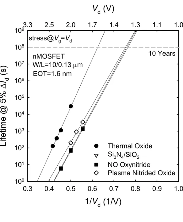
(14) Contents Abstract (Chinese). i. Abstract (English). vi. Acknowledgment (Chinese). x. Contents. xii. Table Captions. xv. Figure Captions. xvi. Chapter 1 1.1. 1.2. Introduction. An Overview of the Background and the Motivation. 1. 1.1.1. MOSFETs with Ultra-Thin Nitrided Gate Oxide. 2. 1.1.2. Strained SiGe Channel MOSFETs. 3. 1.1.3. Ultra-Thin HfO2 Gate Dielectric. 4. Organization of the Thesis. 5. References. 9. Chapter 2. Hot-Electron-Induced Electron Trapping in 0.13 µm nMOSFETs with Ultra-Thin (EOT = 1.6 nm) Nitrided Gate Oxide. 2.1. Introduction. 20. 2.2. Device Fabrication and Characteristics Measurement. 21. 2.3. Results and Discussion. 22. 2.3.1. 2.4. I–V Characteristics. 22. 2.3.2 CHE and SHE Stressing. 24. 2.3.3 DCIV Measurement. 27. 2.3.4 Device Lifetime. 28. Summary. 29. xii.
(15) References. Chapter 3. 30. Flicker Noise Characteristics of 0.15 µm MOSFETs with Ultra-Thin (EOT = 1.6 nm) Nitrided Gate Oxide. 3.1. Introduction. 61. 3.2. Device Fabrication and Characteristics Measurement. 62. 3.3. Results and Discussion. 63. 3.4. Summary. 67. References. 69. Chapter 4. Reliability of Strained SiGe Channel pMOSFETs with Ultra-Thin (EOT = 3.1 nm) N2O-Annealed SiN Gate Dielectric. 4.1. Introduction. 81. 4.2. Device Fabrication and Characteristics Measurement. 83. 4.3. Results and Discussion. 84. 4.4. 4.3.1. C−V and I−V Characteristics of pMOSFETs. 84. 4.3.2. CVS and CCS for pMOSCAPs. 85. 4.3.3. HC and NBTI Stressing for pMOSFETs. 86. Summary. 88. References. Chapter 5. 90. Channel Thickness Effect on Strained SiGe Channel pMOSFETs with Ultra-Thin (EOT=3.1 nm) N2O-Annealed SiN Gate Dielectric. 5.1. Introduction. 112. 5.2. Device Fabrication and Characteristics Measurement. 113. 5.3. Results and Discussion. 114. 5.3. Summary. 117 xiii.
(16) References. Chapter 6. 119. Electrical Characteristics of Thin HfO2 Gate Dielectrics Prepared. Using. Different. Pre-Deposition. Surface. Treatments 6.1. Introduction. 132. 6.2. Device Fabrication and Characteristics Measurement. 134. 6.3. Results and Discussion. 135. 6.3.1 TEM and XPS Analysis. 135. 6.3.2 C−V and I−V Characteristics. 136. 6.3.3 Hysteresis. 137. 6.3.4. 140. 6.4. Conduction Mechanism. Summary. 142. References. 144. Chapter 7. Conclusions and Suggestions of Further Study. 7.1. Conclusions. 166. 7.2. Suggestions of Further Study. 171. Vita (Chinese) Publication List. xiv.
(17) Table Captions. Chapter 6. Table. 6.1. Values of A, B, ln(A/B), Rv, and Eh under the conditions of Vinv = +3 V at T = 300 K. The terms A and B are proportionality constants, Rv is the reciprocal voltage constant, and Eh is the activation energy. Table. 6.2. Values of Ea, qVIL, φ1, φ2, and φt for all samples at Vg = +1 V. The term Ea is the activation energy, VIL is the voltage across the interfacial layer, φ1 is the barrier height between the Si substrate and the interfacial layer, φ2 is the barrier between the interfacial layer and HfO2, and φt is the effective energy of the electron traps with respect to the conduction band edge of the HfO2 layer.. xv.
(18) Figure Captions. Chapter 2. Fig. 2.1.. Gate current densities as a function of gate voltage for four different gate dielectrics, and all devices have the same equivalent oxide thickness (EOT) of 1.6 nm.. Fig. 2.2.. Linear (Vd = 0.05 V) Id−Vg characteristics of nMOSFETs (W/L = 10/0.13 µm) with various ultra-thin (EOT = 1.6 nm) gate dielectrics.. Fig. 2.3.. Transconductance versus gate overdrive (Vg − Vt) of nMOSFETs (W/L = 10/0.13 µm) with various ultra-thin (EOT = 1.6 nm) gate dielectrics.. Fig. 2.4.. Substrate current versus gate voltage of nMOSFETs (W/L = 10/0.13 µm) with various ultra-thin (EOT = 1.6 nm) gate dielectrics.. Fig. 2.5.. Linear (Vd = 0.05 V) Id−Vg characteristics of nMOSFETs (W/L = 10/0.13 µm) with an EOT of 1.6 nm thermal and plasma nitrided gate oxide before and after CHE (Vg = Vd = 1.8 V) stressing for 104 seconds.. Fig. 2.6.. Gate leakage currents of nMOSFETs (W/L = 10/0.13 µm) with an EOT of 1.6 nm plasma nitrided gate oxide before and after CHE (Vg = Vd = 1.8 V) stressing for 104 seconds.. Fig. 2.7.. Threshold voltage shift and transconductance reduction as a function of gate voltage with substrate biases of 0 V and −2 V for the 0.13 µm nMOSFET with an EOT of 1.6 nm plasma nitrided gate oxide after being stressed under SHE injection for 104 seconds. The source and drain are grounded.. Fig. 2.8.. Threshold voltage shifts as a function of substrate bias for the 0.13 µm xvi.
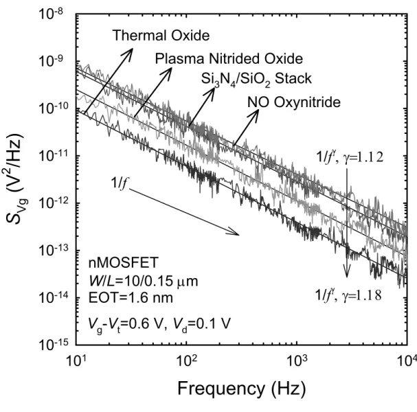
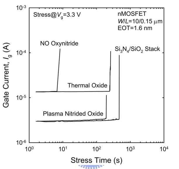
(19) nMOSFETs with various gate dielectrics (EOT = 1.6 nm) after SHE stressing for 104 seconds. The source and drain are grounded. Fig. 2.9.. Schematic band diagram and electron conduction path of n-channel MOSFET as stressed under different substrate bias conditions.. Fig. 2.10. Fig. 2.10. (a) Cross-sectional view and measurement setting of four-terminal n-channel MOSFET used in the DCIV measurement. (b) Base current versus collector-base voltage (Ib–Vcb) for five interface trap distributions, curve-# (drain, channel, source): curve-0 (0, 0, 0), curve-1 (nonuniform, 0, 0), curve-2 (0, uniform, 0), curve-3 (0, nonuniform, 0), and curve-4 (nonuniform, nonuniform, 0). Fig. 2.11. Base currents measured by four-terminal DCIV method of the 0.13 µm nMOSFETs with an EOT of 1.6 nm plasma nitrided gate oxide before and after CHE and SHE stressing for 104 seconds. Fig. 2.12. Threshold voltage shift as a function of stress time of the 0.13 µm nMOSFETs with various gate dielectrics (EOT = 1.6 nm) under SHE stressing (Vg = 2.2 V, Vsub = –1.5 V) for 104 seconds. The source and drain are grounded. Fig. 2.13. Device lifetimes as a function of drain voltage for the 0.13 µm nMOSFETs with various gate dielectrics (EOT = 1.6 nm) under CHE stressing (Vg = Vd).. Chapter 3. Fig. 3.1.. Linear (Vd = 0.1 V) Id−Vg characteristics of 0.15 µm nMOSFETs with various ultra-thin (EOT = 1.6 nm) gate dielectrics.. xvii.
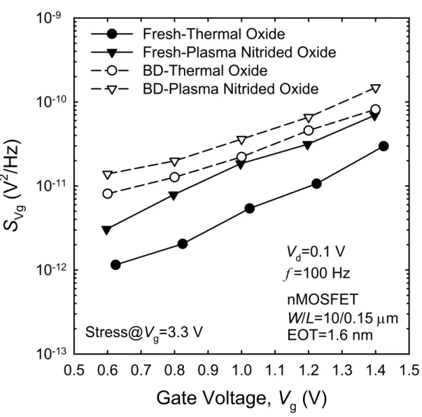
(20) Fig. 3.2.. Transconductance versus gate overdrive (Vg − Vt) of 0.15 µm nMOSFETs with various ultra-thin (EOT = 1.6 nm) gate dielectrics.. Fig. 3.3.. Low-frequency SVg noise power spectra versus frequency at linear operation (Vg − Vt = 1.0 V and Vd = 0.1 V) for 0.15 µm nMOSFETs with various ultra-thin (EOT = 1.6 nm) gate dielectrics.. Fig. 3.4.. Low-frequency SVg noise power spectra (f = 100 Hz) versus gate overdrives (Vg − Vt) at linear operation (Vd = 0.1 V) for 0.15 µm nMOSFETs with ultra-thin (EOT = 1.6 nm) thermal and plasma nitrided gate oxides before and after hot-carrier stressing (Vg = Vd = 2.3 V for 1000 seconds).. Fig. 3.5.. Low-frequency SVg noise power spectra (f = 100 Hz) versus gate overdrives (Vg − Vt) at saturation operation (Vd = 1 V) for 0.15 µm nMOSFETs with ultra-thin (EOT = 1.6 nm) thermal and plasma nitrided gate oxides before and after hot-carrier stressing (Vg = Vd = 2.3 V for 1000 seconds).. Fig. 3.6.. Gate currents versus stress time for 0.15 µm nMOSFETs with various ultra-thin (EOT = 1.6 nm) gate dielectrics stressed at Vg = 3.3 V.. Fig. 3.7.. Low-frequency SVg noise power spectra (f = 100 Hz) versus gate overdrives (Vg − Vt) at linear operation (Vd = 0.1 V) for 0.15 µm nMOSFETs with ultra-thin (EOT = 1.6 nm) thermal and plasma nitrided gate oxides before and after oxide breakdown (Vg = 3.3 V).. Fig. 3.8.. The frequency index of noise spectrum, γ, versus gate voltages for 0.15 µm nMOSFETs with ultra-thin (EOT = 1.6 nm) thermal and plasma nitrided gate oxides before and after hot-carrier stressing (Vg = Vd = 2.3 V for 1000 seconds) and oxide breakdown (Vg = 3.3 V).. xviii.
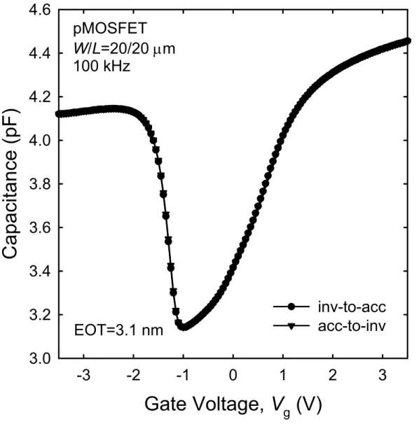
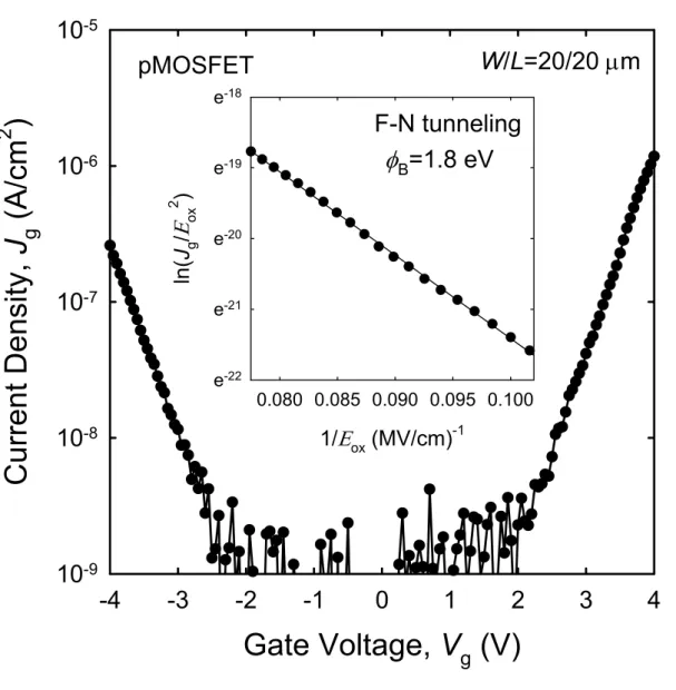
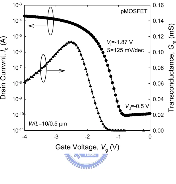
(21) Chapter 4. Fig. 4.1.. The schematic device cross-section and process flow of device fabrication.. Fig. 4.2.. The capacitance–voltage (C–V) characteristics of the pMOSFET with 50 nm Si0.85Ge0.15 channel and N2O-annealed SiN (EOT=3.1 nm) gate dielectric. The equivalent oxide thickness (EOT) of 3.1 nm is extracted from the accumulation capacitance.. Fig. 4.3.. The current–voltage (I–V) characteristics of the pMOSFET with 50 nm Si0.85Ge0.15 channel and N2O-annealed SiN (EOT=3.1 nm) gate dielectric. The inset shows the fitting of Fowler-Nordheim (FN) tunneling with an effective barrier height of 1.8 eV.. Fig. 4.4.. The Id–Vg and Gm characteristics of SiGe pMOSFET (W/L=10/0.5 µm) with N2O-annealed SiN gate dielectric.. Fig. 4.5.. The Id–Vd characteristics of SiGe pMOSFET (W/L=10/0.5 µm) with N2O-annealed SiN gate dielectric with various gate overdrives (Vg–Vt) from 0 to –2 V.. Fig. 4.6.. The C–V characteristics of SiGe pMOSCAP with N2O-annealed SiN gate dielectric for various CVS conditions.. Fig. 4.7.. The leakage current versus the stress time of SiGe pMOSCAP with N2O-annealed SiN gate dielectric under the constant voltage stress (CVS).. Fig. 4.8.. The C–V characteristics of SiGe pMOSCAP with N2O-annealed SiN gate dielectric for various CCS conditions.. Fig. 4.9.. The leakage current versus the stress time of SiGe pMOSCAP with N2O-annealed SiN gate dielectric under the constant current stress (CCS).. Fig. 4.10. The Id degradation versus the stress time of HC and NBTI stressing for the. xix.
(22) SiGe pMOSCAP with N2O-annealed SiN gate dielectric. Fig. 4.11. The Gm degradation versus the stress time of HC and NBTI stressing for the SiGe pMOSCAP with N2O-annealed SiN gate dielectric. Fig. 4.12. The threshold voltage shift (∆Vt) versus the stress time for the SiGe pMOSCAP with N2O-annealed SiN gate dielectric. Fig. 4.13. The charge pumping currents of the devices before and after being stressed at HC and NBTI (RT) stressing. Fig. 4.14. The enlargement of the charge pumping currents shown in Fig. 4.13. Fig. 4.15. Comparison of the interface state generation (∆Nit) which are extracted from the increase of charge pumping currents for the HC and NBTI (RT) stressing. Fig. 4.16. The Id degradation versus the stress time for the channel-hot-carrier stressing under various bias conditions of Vg = Vd = –4.5, –5, and –5.3 V. Fig. 4.17. The Gm degradation versus the stress time for the channel-hot-carrier stressing under various bias conditions of Vg = Vd = –4.5, –5, and –5.3 V. Fig. 4.18. The threshold voltage shift (∆Vt) versus the stress time for the channel-hot-carrier stressing under various bias conditions of Vg = Vd = –4.5, –5, and –5.3 V.. Chapter 5. Fig. 5.1.. SIMS profiles of the SiGe channel in-situ doped with phosphorus.. Fig. 5.2.. The C–V characteristics of the pMOSFETs with different SiGe channel thickness.. Fig. 5.3.. The Id–Vg characteristics of the pMOSFETs with different SiGe channel xx.
(23) thickness. Fig. 5.4.. The Id–Vd characteristics of the pMOSFETs with different SiGe channel thickness.. Fig. 5.5.. The charge pumping currents of the the pMOSFETs with different SiGe channel thickness.. Fig. 5.6.. The interface state density determined by the charge pumping technique and the subthreshold swing of pMOSFETs with different SiGe channel thickness.. Fig. 5.7.. The gate-induced-drain-leakage (GIDL) of the pMOSFETs with different SiGe channel thickness.. Fig. 5.8.. The junction leakage of the pMOSFETs with different SiGe channel thickness.. Fig. 5.9.. The transconductance of the Si channel pMOSFET and the SiGe channel MOSFETs with different SiGe layer thickness.. Fig. 5.10. The effective hole mobility of the Si channel pMOSFET and the SiGe channel MOSFETs with different SiGe layer thickness.. Chapter 6. Fig. 6.1.. TEM pictures of the cross sections for the HfO2 films with different surface treatments. (a) HF-dipped. (b) NH3-annealed. (c) RTO-treated.. Fig. 6.2.. The XPS spectra of the HfO2 films with different surface treatments.. Fig. 6.3.. The capacitance−voltage (C−V) characteristics of NMIS capacitors prepared by applying the three different surface treatment processes. The equivalent oxide thickness (EOT) was determined by measuring the. xxi.
(24) maximum accumulation capacitance. Fig. 6.4.. The plot of the leakage current as a function of gate voltage for each sample.. Fig. 6.5.. The cumulative distribution of leakage currents at Vg = −2.5 V for capacitors formed by using the three different surface treatment processes.. Fig. 6.6.. Normalized C−V curves with different sweeping voltages for each sample: (a) HF-dipped, (b) NH3-annealed, and (c) RTO-treated samples. Initial inversion biases (Vinv) are +1, +2, and +3 V, and the accumulation bias (Vacc) is −3 V.. Fig. 6.7.. The dependence of hysteresis width on the inversion bias (Vinv) during C−V measurement. The reciprocal voltage constant (Rv) is obtained from the slope of the fitted line.. Fig. 6.8.. The plot of hysteresis as a function of the reciprocal of temperature. The activation energy (Eh) for each sample is ca. 0.092 eV.. Fig. 6.9.. The plot of hysteresis as a function of the C−V measuring frequency.. Fig. 6.10. The plot of leakage current as a function of gate voltage as the temperature was varied from 20 to 125 ºC. (a) HF-dipped, (b) NH3-annealed, and (c) RTO-treated samples. Fig. 6.11. The Arrhenius plot of leakage currents at Vg = 1.0 V and Vg = 2.5 V. The activation energy (Ea) increases as the temperature decreases.. Chapter 7. Fig. 7.1.. The schematic device structure of the advanced sub-100 nm SOI MOSFETs with strained layer channel, metal S/D, high-k gate dielectric,. xxii.
(25) and metal gate electrode.. xxiii.
(26) Chapter 1 Introduction 1.1 An Overview of the Background and the Motivation. As predicted by the ITRS [1], the thickness of the gate oxide should be unavoidably less than 1.5 nm for the purpose of gaining performance and eliminating deleterious short channel effects when the channel length of the CMOS devices continuously shrinks below 100 nm. With such thin gate oxide, the intolerable large direct tunneling current [2] and severe boron penetration [3] will become the most severe problems. Many techniques for introducing nitrogen into ultra-thin gate oxide have been demonstrated being capable of considerably alleviating these issues [4]–[10]. On the other hand, the velocity saturation [11], ballistic effect [12]–[15], and the increase of Ioff leakage current [16] may eventually limit the driving capability and device performance with the gate length scaling to the sub-100 nm regime. Hence, the strained layer [17]–[20] are applied to be the device channel for further enhancing the performance of the deep sub-micron device because of the higher carrier mobility [21], [22]. Moreover, the ultra-thin high-k gate dielectrics are recently paid more attention and extensively studied in order to further reduce the leakage current of the tunneling gate oxide [23]–[26]. Therefore, we are interesting in electrical characteristics and reliability of the deep sub-micron MOSFETs fabricated with advanced technologies of ultra-thin nitrided gate oxide, strained SiGe channel, and ultra-thin high-k gate dielectrics.. 1.
(27) 1.1.1 MOSFETs with Ultra-Thin Nitrided Gate Oxide. It is well-known that the nitridation of thermal oxide has been studied for over three decades because of the higher dielectric constant and strength, smaller radiation-induced damages, and enhanced endurance under high-field stress, and numerously various techniques of nitridation have been published, such as oxidation of nitrogen-implanted silicon substrate [27], thermal nitridation with N2 annealing [28], NH3 annealing [29], N2O annealing [30], [31], and NO annealing [32], [33], JVD nitridation [34], remote plasma nitridation (RPN) [35], [36], decoupled plasma nitridation (DPN) [37], reoxidation of nitrided oxide [38], Si3N4/SiO2 (N/O) stack [39], [40]. Many researches have been aggressively conducted in reducing the direct tunneling current and improving the boron penetration by incorporating nitrogen into the sub-2 nm gate oxide [8], [41], [42]. However, thermal nitridation process requires higher temperature to incorporate sufficient nitrogen concentration into the gate oxide [4], and high process temperature makes device integration more difficult as the technology scales down continuously to the sub-100 nm regime. On the other hand, device degradation by hot-carrier stressing is one of the most important reliability issues for short channel MOSFETs, because device characteristics will be degraded by interface-state generation and transconductance reduction [43]. For worse cases, hot-carrier stressing may damage gate oxide to cause oxide breakdown [44]. Although the improvement of hot-carrier reliability achieved by nitrided oxide has been reported [45]–[47], controversial issues are also arisen. Nitrogen incorporation induced positive fixed oxide charges and electron traps are the main concerns for nitrided oxides. Carrier injection and trapping in the gate oxide and transconduction degradation by Coulomb scattering make the hot-carrier degradation still be a significant reliability issue for devices with ultra-thin nitrided gate oxide [48], 2.
(28) [49]. In addition, the low-frequency flicker noise has been regarded as an important consideration in analog and RF device applications [50], and it has also been reported to be another problem for the nitrided gate oxide [51], [52]. Because the flicker noise is believed to be caused by the fluctuation in the number of carriers and/or in carrier mobility which are induced by electron trapping/detrapping through the oxide traps and the mobility scattering when electrons are transporting through the surface channel of MOSFETs [53], the additional electron traps induced by the nitrogen incorporation may enhanced the noise level. Therefore, for the deep sub-micron MOSFETs with ultra-thin nitrided gate oxides, the device degradation of hot-carrier stressing and the flicker noise characteristics should be further investigated.. 1.1.2 Strained SiGe Channel MOSFETs. It has been demonstrated that the strained layer as the channel may dramatically improve the device performance because of the higher carrier mobility [17]–[22]. The strained SiGe channel device, especially for pMOSFET, is, however, more attractive since SiGe has higher bulk carrier mobility than Si [11], the offset of valence band with respect to Si substrate leads to the quantum confinement effect of holes [21], [54], and the induced compressive strained in the SiGe channel would further enhance the channel hole mobility when the SiGe layer is directly on the Si substrate [21], [55]. Moreover, the SiGe device has several attractive merits in device fabrication because of the capability of selective deposition on Si substrate, the completely comparable process with the conventional Si device, and the low activation temperature due to the high dopant activation rate [56]. On the other hand, several drawbacks for the SiGe channel device have also been 3.
(29) proposed [54], [57]–[59]. For example, the lattice mismatch between SiGe and Si interface may induce dislocations, the Ge segregation and atom-induced scattering may degrade the mobility, and lacking a high quality gate insulator for MOS applications. Hence, low temperature process and Si capping layer have to be developed for fabricating SiGe MOSFETs [60]. Additionally, ultra-thin silicon nitride (SiN) has been reported as the promising alternative of gate dielectric for the SiGe channel MOSFETs [61]. Although SiN film usually shows a considerable amount of fixed oxide charges, electron traps, and the interface states to degrade the device performance, N2O-annealing has been proposed to improve the film quality and the interface [62]. However, the device characteristics of the SiGe channel MOSFET with N2O-annealed SiN gate dielectric have not been demonstrated yet so far. Therefore, for deep sub-micron MOSFET applications, the film quality of the ultra-thin N2O-annealed SiN gate dielectric and the strained SiGe channel, the electrical characteristics, and the device reliability still need further extensive study.. 1.1.3 Ultra-Thin HfO2 Gate Dielectric. The high-k metal oxide insulators have been shown to be capable of significantly suppressing the gate leakage current for the same equivalent oxide thickness (EOT) with conventional SiO2-based gate oxides because of their greater physical thickness. The high-k materials therefore have attracted considerable attention as the promising candidate for the ultra-thin gate dielectrics when the gate oxide thickness is scaled down to below 1.5 nm, such as TiO2 [63], Ta2O3 [64], Al2O3 [65], ZrO2 [66], HfO2 [67], La2O3 [68], Y2O3 [69] and Pr2O3 [70]. Among these candidates, HfO2 not only have relatively high dielectric constant and wide band gap [71] but also displays 4.
(30) impressive thermal stability when it directly contacts with the silicon substrate [72]. Therefore, HfO2 film seems to be a good alternative gate dielectric for the generation of sub-1.5 nm gate oxide, and the excellent electrical properties have also been demonstrated [73]. However, the formation of the interfacial layer and the degradation of mobility are still the challenging issues of the MOSFETs with HfO2 gate dielectric, and recently the Hf silicate and nitrogen incorporation are extensively studied to overcome these issues [74]–[76]. Moreover, oxide traps existing in high-k gate dielectrics have been demonstrated as another concerning issue because of the threshold voltage instability [77] and the reliability degradation [78]. To improve the interface quality, pre-deposition surface treatment should be a viable approach and it may also suppress the formation of the interfacial layer. For example, surface nitridation can provide better thermal stability and reliability because of the excellent barrier for interfacial reaction and dopant diffusion and the effective reduction of leakage current [79], and the surface oxidation can be an effective method for reducing the leakage current and improving the quality of the interface [80]. However, both techniques have disadvantages. Nitrogen incorporation may induce extra oxide charges in the gate dielectric to cause a shift in the flat-band voltage. On the other hand, the low dielectric constant of the forming SiO2 layer may increase the EOT and then limit the gate oxide scaling. Therefore, the electrical characteristics of the ultra-thin HfO2 gate dielectrics with different surface treatments have to be further investigated and compared.. 1.2 Organization of the Thesis. Three main topics are investigated and discussed in this dissertation. First, the. 5.
(31) effect of hot-electron-induced electron trapping on device reliability and the low-frequency flicker noise characteristics for the deep sub-micron nMOSFETs with ultra-thin nitrided gate oxides are investigated. Second, the device degradation mechanism and the channel thickness effect on device characteristics for the deep sub-micron strained SiGe channel pMOSFETs with ultra-thin N2O-annealed SiN gate dielectric are studied. Third, the electrical characteristics of the ultra-thin HfO2 gate dielectrics prepared using various pre-deposition surface treatments are compared and discussed. This dissertation is also divided into seven chapters. In Chapter 1, a brief overview of the background and the motivation are introduced. Three main advanced technologies for deep sub-micron MOSFETs are reviewed and we also discuss the most important issues for each technology. In Chapter 2, the hot-electron degradation of the 0.13 µm nMOSFETs with various ultra-thin gate oxides (EOT = 1.6 nm), including thermal oxide, Si3N4/SiO2 stack, NO oxynitride, and plasma nitrided oxide, are investigated. Severe hot-electron degradations under both channel hot-electron and substrate hot-electron injections are observed for the nitrided oxide devices comparing with the thermal oxide device. We also found that the main mechanism responsible for the hot-electron degradation should be dominated by the electron trap generation rather than the interface state generation in the ultra-thin nitrided gate oxides. In Chapter 3, we investigated the low-frequency flicker noise characteristics of the 0.15 µm nMOSFETs with ultra-thin (EOT = 1.6 nm) gate oxides of thermal oxide, Si3N4/SiO2 stack, NO oxynitride, and plasma nitrided oxide subjecting to the hot-carrier stressing and the occurrence of oxide breakdown. The nitrogen incorporation in the ultra-thin gate oxide may increase the noise level by introducing electron traps but improve the device immunity against the hot-carrier degradation in the flicker noise. Comparing with the thermal oxide device, moderate increase of the 6.
(32) noise level for the nitrided oxide devices is observed when oxides are suffering breakdown. We also found that the frequency index of the noise spectrum is varied with the gate bias and decreased by hot-carrier degradation and oxide breakdown. In Chapter 4, we have fabricated the pMOSFETs with 50-nm thick strained Si0.85Ge0.15 channel and ultra-thin (EOT = 3.1 nm) N2O-annealed SiN gate dielectric and investigated the device degradations of the hot-carrier and the negative-bias temperature-instability stressing. The excellent quality of the ultra-thin N2O-annealed SiN gate dielectric is obtained. The experimental results indicate that the hot-carrier degradation is worse than the NBTI degradation and the channel hot-carrier stressing is the worst case for all kinds of reliability testing. We have also verified that the interface state generation should be the main mechanism responsible for the hot-carrier degradation while the electron trapping dominates the device degradation for the NBTI stressing. In Chapter 5, we have fabricated the strained Si0.85Ge0.15 channel pMOSFETs with ultra-thin (EOT = 3.1 nm) N2O-annealed SiN gate dielectric and different channel thickness of 5, 15, and 30 nm. We have found that the thickness of SiGe channel has a great impact on the device characteristics. The thinner SiGe channel devices have been demonstrated to have higher interface quality, better device performance, lower leakage current, and higher mobility than the 30 nm SiGe channel device. In Chapter 6, we have investigated the electrical characteristics of ultra-thin HfO2 gate dielectrics with various pre-deposition surface treatments, such as HF dipping, NH3 surface nitridation, and rapid thermal oxidation. The NH3 nitridation technique has been shown to be superior to other surface treatment techniques. The dependence of hysteresis on the initial inversion bias, temperature, and frequency are also investigated. The hysteresis width is found to be increased with increasing the initial inversion bias and decreased with the temperature, and it is insensitive to the 7.
(33) measuring frequency. The experimental results also indicate that the hysteresis width is exponentially dependent on both the initial inversion bias and the temperature and can be described by an empirical relationship in the form C (T ) ⋅ exp( RvVinv ) . The trap-assisted tunneling is also verified as the dominant conduction mechanism of the ultra-thin HfO2 gate dielectrics. In Chapter 7, we conclude our results and summarize the main conclusions in a list, and the suggestions for further studies are also discussed.. 8.
(34) References. [1]. International Technology Roadmap for Semiconductors, 2004.. [2]. S. H. Lo, D. A. Buchanan, Y. Taur, and W. Wang, “Quantum-mechanical modeling of electron tunneling current from the inversion layer of ultra-thin-oxide nMOSFET's,” IEEE Electron Device Lett., vol. 18, p. 209, 1997.. [3]. R. B. Fair, “Anomalous B penetration through ultrathin gate oxides during rapid thermal annealing,” IEEE Electron Device Lett., vol. 20, p. 466, 1999.. [4]. E. P. Gusev, H. C. Lu, E. L. Garfunkel, T. Gustafsson, and M. L. Green, “Growth and characterization of ultrathin nitrided silicon oxide films,” IBM J. Res. Develop., vol. 43, p. 265, 1999.. [5]. C. H. Chen, Y. K. Fang, S. F. Ting, W. T. Hsieh, C. W. Yang, T. H. Hsu, M. C. Yu, T. L. Lee, S. C. Chen, C. H. Yu, and M. S. Liang, “Downscaling limit of equivalent oxide thickness in Formation of ultrathin gate dielectric by thermal-enhanced remote plasma nitridation,” IEEE Trans. Electron Devices, vol. 49, p. 840, 2002.. [6]. S. Inaba, T. Shimizu, S. Mori, K. Sekine, K. Saki, H. Suto, H. Fukui, M. Nagamine, M. Fujiwara, T. Yamamoto, M. Takayanagi, I. Mizushima, K. Okano, S. Matsuda, H. Oyamatsu, Y. Tsunashima, S. Yamada, Y. Toyoshima, and H. Ishiuchi, “Device Performance of Sub-50 nm CMOS with Ultra-Thin Plasma Nitrided Gate Dielectrics, “ IEDM Tech. Dig., p. 651, 2002.. [7]. H. Niimi and G. Lucovsky, “Monolayer-level controlled incorporation of nitrogen at Si-SiO2 interfaces using remote plasma processing,” J. Vac. Sci. Technol. A, vol. 17, p. 3185, 1999.. 9.
(35) [8]. C. H. Chen, Y. K. Fang, C. W. Yang, S. F. Ting, Y. S. Tsair, M. C. Yu, T. H. Hou, M. F. Wang, S. C. Chen, C. H. Yu, and M. S. Liang, “Thermally-enhanced remote plasma nitrided ultrathin (1.65 nm) gate oxide with excellent performances in reduction of leakage current and boron diffusion,” IEEE Electron Device Lett., vol. 22, p. 378, 2001.. [9]. S. Song, H. J. Kim, J. Y. Yoo, J. H. Yi, W. S. Kim, N. I. Lee, K. Fujihara, H. K. Kang, and J. T. Moon, “On the gate oxide scaling of high performance CMOS transistors,” IEDM Tech. Dig., p. 55, 2001.. [10]. V. Misra, H. Lazar, Z. Wang, Y. Wu, H. Niimi, G. Lucovsky, J. J. Wortman, and J. R. Hauser, “Interfacial properties of ultrathin pure silicon nitride formed by remote plasma enhanced chemical vapor deposition,” J. Vac. Sci. Technol. B, vol. 17, p. 1836, 1999.. [11]. S. M. Sze, Physics of Semiconductor Devices, Wiley, New York, 1981.. [12]. K. Natori, “Ballistic metal-oxide-semiconductor field effect transistor,” J. Appl. Phys., vol. 76, p. 4879, 1994.. [13]. P. M. Solomon and S. E. Laux, “The ballistic FET: Design, capacitance and speed limit,” IEDM Tech. Dig., p. 95, 2001.. [14]. Z. Ren, R. Venugopal, S. Datta, M. Lundstrom, D. Jovanovic, and J. G. Fossum, “The ballistic nanotransistor: A simulation study,” IEDM Tech. Dig., p. 715, 2000.. [15]. F. Assad, Z. Ren, D. Vasileska, S. Datta, and M. S. Lundstrom, “On the performance limits for Si MOSFET’s: A theoretical study,” IEEE Trans. Electron Devices, vol. 47, p. 232, 2000.. [16]. L. Chang, S. Tang, T. J. King, J. Bokor, and C. Hu, “Gate length scaling and threshold voltage control of double-gate MOSFETs,” IEDM Tech. Dig., p. 719, 2000. 10.
(36) [17]. J. L. Hoyt, H. M. Nayfeh, S. Eguchi, I. Aberg, G. Xia, T. Drake, E. A. Fitzgerald, and D. A. Antoniadis, “Strained silicon MOSFET technology,” IEDM Tech. Dig., p. 23, 2002.. [18]. H. C. H. Wang, Y. P. Wang, S. J. Chen, C. H. Ge, S. M. Ting, J. Y. Kung, R. L. Hwang, H. K. Chiu, L. C. Sheu, P. Y. Tsai, L. G. Yao, S. C. Chen, H. J. Tao, Y. C. Yeo, W. C. Lee, and C. Hu, “Substrate-strained silicon technology: Process integration,” IEDM Tech. Dig., p. 61, 2003.. [19]. T. Sanuki, A. Oishi, Y. Morimasa, S. Aota, T. Kinoshita, R. Hasumi, Y. Takegawa, K. Isobe, H. Yoshimura, M. Iwai, K. Sunouchi, and T. Noguchi, “Scalability of strained silicon CMOSFET and high drive current enhancement in the 40nm gate length technology,” IEDM Tech. Dig., p. 65, 2003.. [20]. I. Aberg, C. N. Chléirigh, O. O. Olubuyide, X. Duan, and J. L. Hoyt, “High electron and hole mobility enhancements in thin-body strained Si/strained SiGe/strained Si Heterostructures on insulator,” IEDM Tech. Dig., p. 173, 2004.. [21]. Y. C. Yeo, Q. Lu, T. J. King, C. Hu, T. Kawashima, M. Oishi, S. Mashiro, and J. Sakai, “Enhanced performance in sub-100 nm CMOSFETs using strained epitaxial silicon-germanium,” IEDM Tech. Dig., p. 753, 2000.. [22]. K. Uchida1, R. Zednik, C. H. Lu, H. Jagannathan, J. McVittie, P. C. Mclntyre, and Y. Nishi, “Experimental study of biaxial and uniaxial strain effects on carrier mobility in bulk and ultrathin-body SOI MOSFETs,” IEDM Tech. Dig., p. 229, 2004.. [23]. H. Iwai, S. Ohmi, S. Akama, C. Ohshima, A. Kikuchi, I. Kashiwagi, J. Taguchi, H. Yamamoto, J. Tonotani, Y. Kim, I. Ueda, A. Kuriyama, and Y. Yoshihara, “Advanced gate dielectric materials for sub-100 nm CMOS,” 11.
(37) IEDM Tech. Dig., p. 625, 2002. [24]. J. C. Lee, H. J. Cho, C. S. Kang, S. J. Rhee, Y. H. Kim, R. Choi, C. Y. Kang, C. H. Choi, and M. Akbar, “High-K dielectrics and MOSFET characteristics,” IEDM Tech. Dig., p. 95, 2003.. [25]. H. Y. Yu, J. F. Kang, J. D. Chen, C. Ren, Y. T. Hou, S. J. Whang, M. F. Li, D. S. H. Chan, K. L. Bera, C. H. Tung, A. Du, D. L. Kwong, “Thermally robust high quality HfN/HfO2 gate stack for advanced CMOS devices,” IEDM Tech. Dig., p. 99, 2003.. [26]. T. Watanabe, M. Takayanagi, K. Kojima, K. Sekine, H. Yamasaki, K. Eguchi, K. Ishimaru, and H. Ishiuchi, “Impact of Hf concentration on performance and reliability for HfSiON-CMOSFET,” IEDM Tech. Dig., p. 507, 2004.. [27]. Q. Xu, H. Qian, Z. Han, G. Lin, M. Liu, B. Chen, C. Zhu, and D. Wu, “Characterization of 1.9- and 1.4-nm ultrathin gate oxynitride by oxidation of nitrogen-implanted silicon substrate,” IEEE Trans. Electron Devices, vol. 51, p. 113, 2004.. [28]. M. L. Green, T. Sorsch, L. C. Feldman, W. N. Lennard, E. P. Gusev, E. Garfunkel, H. C. Lu, and T. Gustafsson, “Ultrathin SiOxNy by rapid thermal heating of silicon in N2 at T = 760-1050 °C,” Appl. Phys. Lett., vol. 71, p. 2978, 1997.. [29]. I. J. R. Baumvol, F. C. Stedile, J. J. Ganem, I. Trimaille, and S. Rigo, “Thermal nitridation of SiO2 with ammonia,” J. Electrochem. Soc., vol. 143, p. 2938, 1996.. [30]. H. Huang, W. Ting, D. L. Kwong, and J. Lee, “Electrical and reliability characteristics of ultrathin oxynitride gate dielectric prepared by rapid thermal processing in N2O,” IEDM Tech. Dig., p. 421, 1990.. [31]. P. J. Tobin, Y. Okada, S. A. Ajuria, V. Lakhotia, W. A. Feil, and R. I. Hedge, 12.
(38) “Furnace formation of silicon oxynitride thin dielectrics in N2O,” J. Appl. Phys., vol. 75, p. 1811, 1994. [32]. Y. Okada, P. J. Tobin, and S. A. Ajuria, “Furnace growth silicon oxynitrides using NO,” IEEE Trans. Electron Devices, vol. 41, p. 1608, 1994.. [33]. M. Bhat, J. Kim, J. Yan, G. W. Yoon, K. Han, and D. L. Kwong, “MOS characteristics of ultrathin NO-grown oxynitrides,” IEEE Electron Device Lett., vol. 15, p. 421, 1994.. [34]. Y. C. Yeo, Q. Lu, W. C. Lee, T. J. King, C. Hu, X. Wang, X. Guo, and T. P. Ma, “Direct tunneling gate leakage current in transistors with ultrathin silicon nitride gate dielectric,” IEEE Electron Device Lett., vol. 21, p. 116, 2000.. [35]. G. Lucovsky, “Ultra-thin nitrided gate dielectrics: Plasma processing, chemical characterization, performance, and reliability,” IBM J. Res. Develop., vol. 43, p. 301, 1999.. [36]. S. F. Ting, Y. K. Fang, C. H. Chen, C. W. Yang, W. T. Hsieh, J. J. Ho, M. C. Yu, S. M. Jang, C. H. Yu, M. S. Liang, S. Chen, and R. Shih, “The effect of remote plasma nitridation on the integrity of the ultrathin gate dielectric films in 0.13 µm CMOS technology and beyond,” IEEE Electron Device Lett., vol. 22, p. 327, 2001.. [37]. H.-H. Tseng, Y. Jeon, P. Abramowitz, T. -Y. Luo, L. Hebert, J. J. Lee, J. Jiang, P. J. Tobin, G. C. F. Yeap, M. Moosa, J. Alvis, S. G. H. Anderson, N. Cave, T. C. Chua, A. Hegedus, G. Miner, J. Jeon, and A. Sultan, “Ultra-thin decoupled plasma nitridation (DPN) oxynitride gate dielectric for 80-nm advanced technology,” IEEE Electron Device Lett., vol. 23, p. 704, 2002.. [38]. T. Hori, H. Iwasaki, and K. Tsuji, “Electrical and physical properties of ultrathin reoxidized nitrided oxides prepared by rapid thermal processing,” IEEE Trans. Electron Devices, vol. 36, p. 340, 1989. 13.
(39) [39]. Y. Shi, X. Wang, and T. P. Ma, “Tunneling leakage current in ultrathin (<4 nm) nitride/oxide stack dielectrics,” IEEE Electron Device Lett., vol. 19, p. 388, 1998.. [40]. C. G. Parker, G. Lucovsky, and J. R. Hauser, “Ultrathin oxide-nitride gate dielectric MOSFET’s,” IEEE Electron Device Lett., vol. 19, p. 106, 1998.. [41]. H. Yang and G. Lucovsky, “Integration of ultrathin (1.6 ~ 2.0 nm) RPECVD oxynitride gate dielectrics into dual poly-Si gate submicron CMOSFETs,” IEDM Tech. Dig., p. 245, 1999.. [42]. C. H. Chen, Y. K. Fang, C. W. Yang, S. F. Ting, Y. S. Tsair, M. F. Wang, Y. M. Lin, M. C. Yu, S. C. Chen, C. H. Yu, and M. S. Liang, “High-quality ultrathin (1.6 nm) nitride/oxide stack gate dielectrics prepared by combining remote plasma nitridation and LPCVD technologies,” IEEE Electron Device Lett., vol. 22, p. 260, 2001.. [43]. J. E. Chung, P. K. Ko, and C. Hu, “A Model for hot-electron-induced MOSFET linear-current degradation based on mobility reduction due to interface-state generation,” IEEE Trans. Electron Devices, vol. 38, no. 6, p. 1362, June 1991.. [44]. K. Umeda and K. Taniguchi, “Hot-electron-induced quasibreakdown of thin gate oxides,” J. Appl. Phys., vol. 82, p. 297, 1997.. [45]. T. Hori and H. Iwasaki, “Improved hot-carrier immunity in submicrometer MOSFET’s with reoxidized nitrided oxides prepared by rapid thermal processing,” IEEE Electron Device Lett., vol. 10, p. 64, 1989.. [46]. H. S. Momose, T. Morimoto, Y. Ozawa, K. Yamabe, and H. Iwai, “An improvement of hot-carrier reliability in the stacked nitride-oxide gate n- and p-MISFET’s,” IEEE Trans. Electron Devices, vol. 42, no. 4, p. 704, April 1995. 14.
(40) [47]. A. B. Joshi, and D. L. Kwong, “Excellent immunity of GIDL to hot-electron stress in reoxidized nitrided gate oxide MOSFET’s,” IEEE Electron Device Lett., vol. 13, p. 47, 1992.. [48]. M. T. Takagi and Y. Toyoshima, “Importance of Si-N atomic configuration at the Si/oxynitride interfaces on the performance of scaled MOSFETs,” IEDM Tech. Dig., p. 575, 1998.. [49]. H. S. Momose, T. Morimoto, Y. Ozawa, K. Yamabe, and H. Iwai, “Electrical characteristics of rapid thermal nitrided-oxide gate n- and p-MOSFET’s with less than 1 atom% nitrogen concentration,” IEEE Trans. Electron Devices, vol. 41, p. 546, 1994.. [50]. Y. Nemirovsky, I. Brouk, and C. G. Jakobson, “1/f noise in CMOS transistors for analog applications,” IEEE Trans. Electron Devices, vol. 48, p. 921, 2001.. [51]. Z. J. Ma, Z. H. Liu, Y. C. Cheng, P. K. Ko, and C. Hu, “New insight into high-field mobility enhancedment of nitrided-oxide N-MOSFET’s based on noise measurement,” IEEE Trans. Electron Devices, vol. 41, p. 2205, 1994.. [52]. H. Wong and Y. C. Cheng, “Gate dielectric-dependent flicker noise in metal-oxide-semiconductor transistors,” J. Appl. Phys., vol. 67, p. 863, 1990.. [53]. K. K. Hung, P. K. Ko, C. Hu, and Y. C. Cheng, “A unified model for the flicker noise in metal-oxide-semiconductor field-effect transistors,” IEEE Trans. Electron Devices, vol. 37, p. 654, 1990.. [54]. R.. People,. “Physics. and. applications. of. GexSi1-x/Si. strained-layer. heterostructures,” IEEE J. of Quantum Electronics, vol. QE-22, p. 1696, 1986. [55]. M. Shima, T. Ueno, T. Kumise, H. Shido, T. Sakuma, and S. Nakamura, “<100> channel strained-SiGe p-MOSFET with enhanced hole mobility and lower parasitic resistance,” Symp. VLSI Tech. Dig., p. 94, 2002.. [56]. T. J. King, J. P. McVittie, K. C. Saraswat, and J. R. Pfiester, “Electrical 15.
(41) properties of heavily doped polycrystalline silicon-germanium films,” IEEE Trans. Electron Devices, vol. 41, p. 228, 1994. [57]. J. C. Bean, L. C. Feldman, A. T. Fiory, S. Nakahara, and I. K. Robinson, “GexSi1-x/Si strained-layer superlattice grown by molecular beam epitaxy,” J. Vac. Sci. Technol. A, vol. 2, p. 346, 1984.. [58]. A. T. Foiry, J. C. Bean, R. Hull, and S. Nakahara, “Thermal relaxation of metalstable strained-layer GexSi1-x/Si epitaxy,” Phys. Rev. B, vol. 13, p. 4063, 1985.. [59]. F. K. LeGoues, R. Rosenberg, T. Nguyen, F. Himpsel, and B. S. Meyerson, “Oxidation studies of SiGe,” J. Appl. Phys., vol. 65, p. 1724, 1989.. [60]. Y. C. Yeo, Q. Lu, T. J. King, C. Hu, T. Kawashima, M. Oishi, S. Mashiro, and J. Sakai, “Enhanced performance in sub-100 nm CMOSFETs using strained epitaxial silicon-germanium, “IEDM Tech. Dig., p. 753, 2000.. [61]. W. Lu, R. Hammond, S. J. Koester, X. W. Wang, J. O. Chu, T. P. Ma, and I. Adesida, “High performance 0.15 µm self-aligned SiGe p-MOS-MODFET’s with SiN gate dielectric,” IEDM Tech. Dig., p. 577, 1999.. [62]. S. Tsujikawa, T. Mine, Y. Shimamoto, O. Tonimura, R. Tsuchiya, K. Ohnishi, H. Hamamura, K. Torii, T. Onai, and J. Yugami, “An ultra-thin silicon nitride gate dielectric with oxygen-enriched interface (OI-SiN) for CMOS with EOT of 0.9 nm and beyond,” Symp. VLSI Tech. Dig., p. 202, 2002.. [63]. X. Guo, X. Wang, Z. Luo, T. P. Ma, and T. Tamagawa, “High quality ultra-thin (1.5 nm) TiO2/Si3N4 gate dielectric for deep sub-micron CMOS technology,” IEDM Tech. Dig., p. 137, 1999.. [64]. H. F. Luan, S. J. Lee, C. H. Lee, S. C. Song, Y. L. Mao, Y. Senzaki, D. Roberts, and D. L. Kwong, “High quality Ta2O5 gate dielectrics with Tox,eq<10Å,” IEDM Tech. Dig., p. 141, 1999. 16.
(42) [65]. D. A. Buchanan, E. P. Gusev, E. Cartier, H. O. Schmidt, K. Rim, M. A. Gribelyuk, A. Mocuta, A. Ajmera, M. Copel, S. Guha, N. Bojarczuk, A. Callegari, C. D'Emic, P. Kozlowski, K. Chan, R. J. Fleming, P. C. Jamison, J. Brown, and R. Arndt, “80 nm Poly-silicon gated n-FETs with ultra-thin Al2O3 gate dielectric for ULSI applications,” IEDM Tech. Dig., p. 223, 2000.. [66]. W. J. Qi, R. Nieh, B. H. Lee, L. Kang, Y. Jeon, K. Onishi, T. Ngai, S. Banerjee, and J. C. Lee, “MOSCAP and MOSFET characteristics using ZrO2 gate dielectric deposited directly on Si,” IEDM Tech. Dig., p. 145, 1999.. [67]. B. H. Lee, L. Kang, W. J. Qi, R. Nieh, Y. Jeon, K. Onishi, and J. C.Lee, “Ultrathin hafnium oxide with low leakage and excellent reliability for alternative gate dielectric application,” IEDM Tech. Dig., p. 133, 1999.. [68]. Y. H. Wu, M. Y. Yang, A. Chin, W. J. Chen, and C. M. Kwei, “Electrical characteristics of high quality La2O3 gate dielectric with equivalent oxide thickness of 5 Å,” IEEE Electron Device Lett., vol. 21, p. 341, 2000.. [69]. L. Manchanda and M. Gurvitch, “Yttrium oxide/silicon dioxide: A new dielectric structure for VLSI/ULSI circuits,” IEEE Electron Device Lett., vol. 9, p. 180, 1988.. [70]. H. J. Osten, J. P. Liu, P. Gaworzewski, E. Bugiel, and P. Zaumseil, “High-k gate dielectrics with ultra-low leakage current based on praseodymium oxide,” IEDM Tech. Dig., p. 653, 2000.. [71]. G. D. Wilk, R. M. Wallace, and J. M. Anthony, “High-k gate dielectrics: Current status and materials properties considerations,” J. Appl. Phys., vol. 89, p. 5243, 2001.. [72]. K. J. Hubbard and D. G. Schlom, “Thermodynamic stability of binary oxides in contact with silicon,” J. Mater. Res., vol. 11, p. 2757, 1996.. [73]. S. Pidin, Y. Morisaki, Y. Sugita, T. Aoyama, K. Irino, T. Nakamura, and T. 17.
(43) Sugii, “Low standby power CMOS with HfO2 gate oxide for 100-nm generation,” Symp. VLSI Tech. Dig., p. 28, 2002. [74]. M. Koyama, A. Kaneko, T. Ino, M. Koike, Y. Kamata, R. Iijima, Y. Kamimuta, A. Takashima, M. Suzuki, C. Hongo, S. Inumiya, M. Takayanagi, and A. Nishiyama, “Effects of nitrogen in HfSiON gate dielectric on the electrical and thermal characteristics,” IEDM Tech. Dig., p. 849, 2002.. [75]. J. C. Lee, H. J. Cho, C. S. Kang, S. Rhee, Y. H. Kim, R. Choi, C. Y. Kang, C. Choi, and M. Abkar, “High-K dielectrics and MOSFET characteristics,” IEDM Tech. Dig., p. 95, 2003.. [76]. M. Koike, T. Ino, Y. Kamimuta, M. Koyama, Y. Kamata, M. Suzuki, Y. Mitani, A. Nishiyama, and Y. Tsunashima, “Effect of Hf-N bond on properties of thermally stable amorphous HfSiON and applicability of this material to sub-50nm technology node LSIs,” IEDM Tech. Dig., p. 107, 2003.. [77]. L. Pantisano, E. Cartier, A. Kerber, R. Degraeve, M. Lorenzini1, M. Rosmeulen, G. Groeseneken, and H. E. Maes, “Dynamics of threshold voltage instability in stacked high-k dielectrics: Role of the interfacial oxide,” Symp. VLSI Tech. Dig., p. 28, 2002.. [78]. W. Y. Loh, B. J. Cho, M. S. Joo, M. F. Li, D. S. H. Chan, S. Mathew, and D. L. Kwong, “Analysis of charge trapping and breakdown mechanism in high-k dielectrics with metal gate electrode using carrier separation,” IEDM Tech. Dig., p. 927, 2003.. [79]. R. Choi, C. S. Kang, B. H. Lee, K. Onishi, R. Nieh, S. Gopalan, E. Dharmarajan, and J. C. Lee, “High-quality ultra-thin HfO2 gate dielectric MOSFETs with TaN electrode and nitridation surface preparation,” Symp. VLSI Tech. Dig., p. 15, 2001.. [80]. Y. Kim, C. Lim, C. D. Young, K. Matthews, J. Barnett, B. Foran, A. Agarwal, 18.
(44) G. A. Brown, G. Bersuker, P. Zeitzoff, M. Gardner, R. W. Murto, L. Larson, C. Metzner, S. Kher, and H. R. Huff, ”Conventional poly-Si gate MOS-transistors with a novel ultra-thin Hf-oxide layer,” Symp. VLSI Tech. Dig., p. 167, 2003.. 19.
(45) Chapter 2 Hot-Electron-Induced Electron Trapping in 0.13. µm nMOSFETs with Ultra-Thin (EOT = 1.6 nm) Nitrided Gate Oxide 2.1 Introduction. The incorporation of nitrogen into the gate oxide has become a viable approach to reduce the intolerably high standby power consumption and overcome boron penetration when the gate oxide of continues to scale down below 2 nm because it provides a physically thicker film with the same electrical equivalent oxide thickness (EOT) for reducing tunneling current and simultaneously suppressing the boron diffusion effectively [1]–[4]. In the past, a variety of techniques including thermal nitridation [5]–[17], jet vapor deposition (JVD) nitride [18]–[22], remote plasma nitridation (RPN) [23]–[28], decoupled plasma nitridation (DPN) [29], [30], and stacked nitride/oxide [31]–[40] have been studied extensively and shown to be beneficial in alleviating the above-mentioned problems. Despite these encouraging results, however, the impacts of nitrogen incorporation on the long-term reliability characteristics of the fabricated devices are still controversial. Some groups have studied that the introduction of nitrogen did cause significant reliability degradation in terms of charge trapping [41]–[45] and hot-carrier immunity[46]–[56], while the others asserted the improved robustness against hot-carrier degradation by employing various nitridation techniques [8], [57]–[69]. In this study, we demonstrate that the 20.
(46) gate dielectrics of 1.6nm EOT with nitrogen incorporation in deep sub-micron nMOSFETs will become less robust against hot-electron striking even though it has been shown that the ultra-thin oxides in direct tunneling regime have better hot-carrier reliability for nMOSFETs [70]–[74]. Several nitrogen incorporation techniques are employed in this work, including stacked Si3N4/SiO2 (N/O), NO annealing, and plasma nitridation. It is clearly observed that 0.13 µm nMOSFETs with ultra-thin nitrided gate oxides (EOT = 1.6 nm) depict much severe degradations under both channel hot-electron (CHE) and substrate hot-electron (SHE) injections as compared to the device with conventional ultra-thin gate oxide. Meanwhile, it is found that the main mechanism which is responsible for the hot-electron degradation should be dominated by the electron trap generation rather than the interface state generation in the ultra-thin nitrided gate dielectrics after the long-term hot-electron stressing.. 2.2 Device Fabrication and Characteristics Measurement. After active region definition, wafers were split to receive various gate dielectric preparation recipes, including thermal oxidation (i.e., control), Si3N4/SiO2 (N/O) stack, NO-annealed oxide, and thermal oxide with plasma nitridation. Thermal oxide was grown by wet oxidation in catalysis oxidation chamber at 800°C; Si3N4/SiO2 stack was made of a 0.8-nm bottom thermal oxide at 800°C followed nitridation in a high-density remote helicon-based nitrogen discharge at 450°C and a 1.4-nm high-quality nitride film deposited by low-pressure chemical-vapor-deposition (LPCVD) using gas sources of SiH4 and NH3 at 800°C; NO-annealed oxide was achieved with annealing the pre-grown thermal oxide at 800°C in the NO ambient; Plasma nitridation was implemented with exposing the thermal oxide to a decouple. 21.
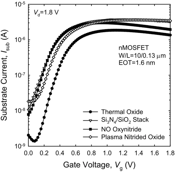
(47) plasma source at 550°C, 20 mTorr, in N2 ambient followed by rapid thermal annealing (RTA) at 1050°C for 10 seconds. All of these gate dielectrics were carefully designed to have the same equivalent oxide thickness (EOT) of approximately 1.6 nm, as identified by C–V measurements. After deposition and patterning of a 150 nm un-doped polysilicon film, arsenic dopants were implanted with the energy of 5 KeV for simultaneous gate electrode doping and shallow source/drain junction formation. For dopant activation, all wafers were annealed by rapid thermal annealing (RTA) in N2 gas ambient for 30 sec. Subsequently, cobalt salicide, PSG, and metallization were performed to complete the device fabrication. The current−voltage (I−V) characteristics were measured by using a Keithley 4200 semiconductor characterization system. Two hot-carrier stressing methods, i.e., CHE and SHE injections, were used for evaluating the device reliability. The indicators of reliability degradation are the reduction of driving current, ∆Id/Id at Vg = Vd = 1 V, and transconductance, ∆Gm/Gm at the peak value, as well as threshold voltage shift (∆Vt). Moreover, the variation of interface states will be monitored by the Direct–Current Current–Voltage (DCIV) method before and after the devices being stressed at CHE and SHE injections.. 2.3 Results and Discussion. 2.3.1 I–V Characteristics. The results of gate leakage current for various ultra-thin gate oxides are shown in Fig. 2.1. Consistent with the previous reports [26], [28], [31], [36], [75]–[83], the gate leakage currents are reduced for all gate oxides with nitrogen incorporation, and 22.
(48) both N/O stack and plasma nitrided gate dielectrics are almost one order of magnitude lower than that of the thermal oxide with the same EOT value of 1.6 nm. The reduction of leakage currents are due to the increase of physical thickness which is achieved by increasing the dielectric constant for the nitrided oxides [84], [85]. Figure 2.2 demonstrates the linear Id−Vg characteristics for 0.13 µm nMOSFETs with various ultra-thin (EOT = 1.6 nm) gate dielectrics. Obviously, we can see that all devices have an almost identical subthrethold swing (S ~ 81 mV/dec), and the threshold voltages are displayed slightly negative shifts for the nitrided oxide devices as compared to the thermal oxide counterpart because of the nitrogen-induced positive charges in the gate dielectrics [30], [38], [47], [52], [65], [67], [86]–[91]. From this viewpoint, NO nitridation technique is the worst because the largest shift of threshold voltage has been observed. In addition, the transconductance versus the gate overdrive (Vg–Vt) for all devices are shown in Fig. 2.3. With respect to the control device with thermal gate oxide, the devices with N/O stack and plasma nitrided gate dielectrics show slight peak degradation of Gm at low gate bias which is attributed to the loss of mobile inversion electrons caught by the additional traps and the consequent Coulomb scattering [35], [47], [92]–[96]. The transconductance is, however, enhanced at high gate voltage regime, which has been reported to be caused by several possible factors: high interfacial nitrogen concentration may induce residual tensile stress at the interface [94], [97], [98], nitrogen incorporation at the interface may reduce the acceptor-like interface states near and above the conduction edge [94], [95], [99], and the electron trapping at the interface traps may screen the surface scattering through Coulomb shielding [35], [95], [100]–[102]. On the other hand, for the device with NO oxynitride, the severe Gm degradation should be due to higher level of nitrogen pile-up near the bottom interface via NO annealing [30], [52], [93], [94], [100], which can also explain the result revealed in Fig. 2.2. 23.
(49) 2.3.2 CHE and SHE Stressing. For the deep sub-micron devices with conventional ultra-thin gate oxide, it has been shown that the worst hot-carrier stress condition switches from Vg = Vd/2 (maximum Isub) to Vg = Vd [103]–[107], and the device degradation is also enhanced by the valence-band electron tunneling when the oxide thickness shrinks down to the direct tunneling regime [105]. For the 0.13 µm nMOSFETs with ultra-thin nitrided gate oxides, as shown in Fig. 2.4, similar flat curves of substrate current versus gate voltage (Ib–Vg) are also obtained, so the worst condition of Vg = Vd was used to monitor the degradations of our devices for hot-carrier stressing. Although the interface state generation has been demonstrated to be the main cause of the hot-carrier degradation for ultra-thin gate oxide devices [72], [104], [105], [108], the situation is, however, quite different for the devices with ultra-thin nitrided gate dielectrics. Figure 2.5 indicates that almost no degradation was observed for the thermal oxide device with an EOT value of 1.6 nm, and this result is consistent with the previous works [70]–[74]. On the other hand, a slightly larger increase of threshold voltage (∆Vt = 6 mV) is presented even though almost unchanged subthreshold swing was also observed for the plasma nitrided oxide device after being stressed under Vg = Vd = 1.8 V (CHE) for 104 seconds. According to the results that nitrided oxide is very resistive to the interface state generation [47], [49], [52]–[54], [57]–[59], [62], [63], [67], we, then, speculate that the electron trapping should be the dominating mechanism of the hot-electron degradation for the ultra-thin nitrided oxide device. Moreover, Fig. 2.6 displays that the gate leakage current of the plasma nitrided oxide is slightly decreased after the CHE stressing. This trend is opposite to the results shown in other works, in which the increase of gate current has been 24.
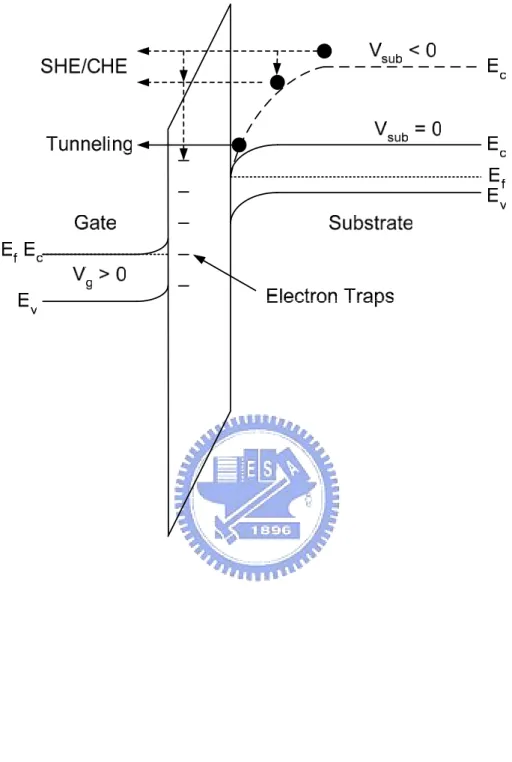
(50) demonstrated if the gate oxide and the interface are damaged [74], [106], [108]–[115]. Therefore, the reduction of gate leakage current is believed to be due to the local electric field lowering induced by the electrons trapped in the gate dielectric [109], [116]. Figure 2.7 depicts the ∆Vt and ∆Gm/Gm versus gate voltage as a function of substrate bias (Vsub) under SHE stressing for the 0.13 mm nMOSFET with plasma nitrided gate oxide. We can clearly see that only negligible degradation has been found even when the gate voltage is up to 2.6 V when Vsub was fixed at 0 V (i.e. constant voltage stress, CVS). For the case of SHE stressing under Vsub = −2 V, however, the ∆Vt as well as ∆Gm/Gm are significantly enhanced with the increase of gate voltage. Note that the channel of device is strongly inverted for all applied gate voltages (Vg > Vt = 0.38 V). Thus, the electron injection into the gate dielectric which degrades threshold voltage (positive shift) and transconductance should be dominated by the substrate bias rather than the gate voltage. These results imply that the degradation must be strongly related to the energy of electrons flowing through the gate dielectric because electrons will gain energy from the substrate bias injection. Interestingly, Vt and Gm degradations are shown in a similar trend which indicates that Vt shift and Gm reduction may be enhanced by the same degradation mechanism, i.e. the electron trapping in the gate dielectric. In addition, the shifts of threshold voltage as a function of substrate bias under SHE stressing for various gate dielectrics are shown in Fig. 2.8. It can be seen that nitrogen-incorporated gate dielectrics depict poorer immunity against SHE stressing. When the substrate bias becomes more negatively than −1 V, all but the control device with thermal oxide show a drastic increase in threshold voltages. These sudden increases in the threshold voltages imply that electron trapping should be the dominant mechanism which is responsible for the aggravated device degradation for all nitrided gate oxide devices. Based on the 25.
數據
+7

相關文件
Promote project learning, mathematical modeling, and problem-based learning to strengthen the ability to integrate and apply knowledge and skills, and make. calculated
volume suppressed mass: (TeV) 2 /M P ∼ 10 −4 eV → mm range can be experimentally tested for any number of extra dimensions - Light U(1) gauge bosons: no derivative couplings. =>
• Formation of massive primordial stars as origin of objects in the early universe. • Supernova explosions might be visible to the most
This kind of algorithm has also been a powerful tool for solving many other optimization problems, including symmetric cone complementarity problems [15, 16, 20–22], symmetric
(Another example of close harmony is the four-bar unaccompanied vocal introduction to “Paperback Writer”, a somewhat later Beatles song.) Overall, Lennon’s and McCartney’s
專案執 行團隊
Microphone and 600 ohm line conduits shall be mechanically and electrically connected to receptacle boxes and electrically grounded to the audio system ground point.. Lines in
Digital PCR works by partitioning a sample into many individual real-time PCR reactions, some portion of these reactions contain the target molecules(positive) while others do
