國立交通大學
光電工程研究所
博士論文
多晶矽薄膜電晶體於主動矩陣式
有機發光二極體顯示器之應用
Applications of Poly-Silicon Thin Film Transistor for
Active-Matrix Organic Light-Emitting Display
研究生:林彥仲
指導教授:謝漢萍教授
多晶矽薄膜電晶體於主動矩陣式
有機發光二極體顯示器之應用
Applications of Poly-Silicon Thin Film Transistor for
Active-Matrix Organic Light-Emitting Display
研究生:林彥仲
Student : Yen-Chung Lin
指導教授:謝漢萍
Advisor : Han-Ping D. Shieh
國立交通大學
光電工程研究所
博士論文
A Thesis
Submitted to Institute of Electro-Optical Engineering
College of Electrical Engineering and Computer Science
National Chiao Tung University
in Partial Fulfillment of the Requirements
for the Degree of Doctor of Philosophy
in
Electro-Optical Engineering
2005
Hsinchu, Taiwan, Republic of China
多晶矽薄膜電晶體於主動矩陣式
有機發光二極體顯示器之應用
博士研究生:林彥仲 指導教授:謝漢萍教授
國立交通大學 光電工程研究所
摘 要
近年來平面顯示技術不論在電腦資訊或家用電視領域上的發展,均大幅吸引 人們的注意,由於平面顯示器具有輕、薄、低功耗、廣視角及全彩化之能力,因 此在各個層面的應用上都具有相當大的潛力。有機發光二極體 OLED (Organic Light Emitting Diode) 因具有低操作電壓與高發光效率的特性的,利用此元件 與技術所製成的顯示器具有輕薄、可撓曲式、易攜性、全彩高亮度、省電、可視 角廣及無影像殘影……等優點,為未來平面顯示器的新趨勢。由於被動矩陣(passive matrix)驅動方式在畫質相較主動矩陣式(active matrix),在解析度、灰階數受到限制且無法實現精細化,因而採用薄膜電晶體 (Thin Film Transistor; TFT)來控製 OLED 元件形成主動矩陣式顯示器,將是高 畫質平面顯示器的趨勢,因為 OLED 是屬於電流驅動的元件,目前使用多晶矽 (Poly-Silicon; poly-Si)技術來製作的薄膜電晶體,其物理特性較非晶矽的薄 膜電晶體要來更好,由於電子移動率較快,不僅在 OLED 的畫素驅動電路上具有 較好的特性,也能將週邊驅動電路一併整合至顯示面板上,以實現高度整合性之 有機發光顯示器。 主動矩陣驅動顯示技術雖然具備實現高解析度顯示器的潛力,但由於 OLED 必須由電流來驅動以產生亮度,因此當 OLED 的電流通過每個畫素電極時,因導 線的寄生電阻造成驅動電壓下降,使得主動矩陣式 OLED 面板仍存在亮度均勻性 不佳的缺點,在本論文研究中則成功開發出「交流電壓驅動方法」來驅動 OLED 畫 素電晶體。此驅動法利用儲存電容的耦合效應,配合交流電壓驅動信號,對導線
寄生電阻所造成的壓降進行補償的動作,經實驗證實顯示器亮度均勻性能有效提 升,此外採用交流驅動方法所製作之面板,在電功率消耗上仍舊能維持與傳統直 流電壓驅動法相同的水準。 在半導體製程中常因環境或人為因素造為元件特性穩定性不足,如 TFT 元件 的閘電壓或是載子遷移率在玻璃基板各處之分布並非一定值,當畫素電路中的 TFT 特性產生漂移時,整體面板的亮度均勻性就受到相當大的影響,在此論文研 究中,我們提出一具備電流驅動能力之 AM-OLED 顯示器,此顯示器中包含了由電 流驅動之畫素電路,以及整合在面板上的電流型式驅動電路,利用高效能之電流 記憶體電路配合參考電流產生器,此整合驅動電路能產生能符合顯示灰階所需的 完整驅動電流,提供給 AM-OLED 畫素電路做為驅動信號,藉此電流驅動方式補償 半導體元件特性漂移之現象,此外整合在基板內之驅動電路具有操作簡單及運作 速度快等優點,利於高解析度 AM-OLED 顯示器之應用。 隨著 OLED 材料不斷進步,所需之驅動電流也逐漸降低,因為傳統的電流驅 動方式在低灰階狀態下會遭遇資料寫入時間不足之現象,在此研究中我們發展一 具有驅動電流放大功能之 AM-OLED 畫素電路,此電路中利用電容耦合之方式,來 放大寫入畫素之資料驅動電流,在不須要增加 TFT 尺寸之下,此畫素電路具有廣 泛的操作範圍,在高灰階狀態下有較低的放大率以避免過高的功率消耗,而當操 作於低灰階狀態時也具有較高的放大率,藉此將輸入電流信號放大以提升信號寫 入速度,同時此電流驅動之畫素電路仍能補償因製程或長時間操作所造成 TFT 之 特性漂移,以實現高均勻性的亮度與畫質。 在畫素電路設計上不僅須考慮顯示畫質均勻性,且必須同時兼顧一畫素陣列 的可測試性,在此論文研究中,我們發展出一新式畫素電路架構,在此架構中僅 額外設計一測試電容於畫素電路當中用來確保畫素電路的完整性,藉此測試電 容,在畫素電路中所有的 TFT 元件及儲存電容均可用偵測儲存電荷的方法來確認 元件的特性與電路的功能。 論文中展現了薄膜電晶體技術在於有機發光顯示器上的重大應用潛力,提供 系統設計者更多的技術來源與設計創意空間來開發更佳的顯像技術,此結合顯示 電路設計與半導體製程的顯示面板開發技術,也將在未來高科技產業中具有益形 重要的地位。
Applications of Poly-Silicon Thin Film Transistor for
Active-Matrix Organic Light-Emitting Display
Doctoral Student: Yen-Chung Lin Advisor: Dr. Han-Ping D. Shieh
Institute of Electro-Optical Engineering National Chiao Tung University
Abstract
In recent years attractions have been made on producing flat panel display to replace the bulky CRT displays for computer monitors and televisions. Displays with the features of light weight, low power, high brightness, wide viewing-angles, and full color are essential for various applications. Combining Organic Light Emitting Devices with poly-Si TFTs to form an AM-OLED is an unique technology to meet those requirements. However, the AM-OLED still has several issues needed to be addressed. This dissertation presents a detailed study of the design of pixel and integrated driver circuitries to improve the image quality, functionality and testability for AM-OLED based on the poly-Si TFT technology.
In this dissertation we successfully developed an AC voltage driving scheme which can improve the brightness uniformity of AM-OLED displays. Through the use of a charge feed-through mechanism and an AC driving voltage, the voltage drop caused by the parasitic resistance can be compensated. A 2.2 inch AM-OLED panel has been improved by the low temperature polycrystalline silicon technology to evaluate the performance of the AC driving scheme. Experimental results show that a brightness uniformity of higher than 91.6% can be achieved by the AC driving scheme, in sharp contrast with 74% achieved by a DC driving scheme.
An integrated driving system including switch-current memory, digital-to-current converter, and reference current generator circuits has been developed for improving the accuracy of data programming and the operating frequency for AM-OLED’s. The proposed switch-current memory, constructed from the current memory structure, can not only reduce the influence of charge-injection without using larger storage capacitor, but also realize the significant improvement in speed by use of small
storage capacitors. Furthermore, the capability of copying the current signal is achieved without relying on the matching of device characteristics. The switch-current memory circuit coordinating with reference current generator to form a digital to current converter is capable of generating accurate data currents for adequate gray scales. The experimental results not only demonstrate an achievement of uniform display luminance but also show great potential for high-resolution AM-OLED based on the current driving scheme.
A poly-Si TFT based pixel electrode circuit with a function of current scaling is proposed for AM-OLED’s in this dissertation. In contrast to the conventional current mirror pixel electrode circuit, a high current scaling ratio can be achieved by using a cascade structure of storage capacitors, without increasing the size of the driving TFT in the pixel. Moreover, the proposed pixel circuit can also compensate for the variations of the TFT threshold voltage. Simulation results, based on poly-Si TFT and OLED experimental data, showed that a current scaling ratio of larger than 10 and a fast pixel programming time can be accomplished with the proposed circuit.
In this dissertation we present a functional testing scheme using a two TFT pixel electrode circuit of AM-OLED displays. This pixel circuit and the co-operative charge sensing scheme can not only evaluate the characteristics of each TFT, but also determine the location of line and point defects in the TFT array. Information on defects can be used in the repair system for cutting and repairing these defects. Furthermore, the functional testing scheme can be applied as a part of yield management of the AMOLED array process.
This dissertation has successfully demonstrated the great potentials of integrated driving circuits implemented by poly-Si TFT technology for portable AM-OLED applications. By using semiconductor process to fabricate AM-OLED panels with integrated current driving systems, the AM-OLED’s are appealing for variety of novel applications in the near future.
誌 謝
在交大的兩千一百個日子,伴隨著歡笑與汗水度過,雖然如今輕舟已過萬重 山,但一路行來,許多人的扶持與提攜,讓我永遠銘記在心,雖然這不是一部完 美的論文,但這部論文的完成,要感謝的真的人很多,在此僅以此文表達我的誠 摯謝意。 首先要感謝的是我的指導教授謝漢萍博士,引領我進入學術的殿堂,將近六 年的時光中,除了培養我在研究上獨立思考和創新的精神外,也教導了許多做人 處事的道理,讓我了解到不論在學術或是人生的任何事上,都要以嚴謹認真的態 度來面對,每當我遇到瓶頸時,總是給我很大的支持,使我能堅持到底。而在論 文過程中要感謝每位口試委員的悉心指導以及研究方法上的指教,使得我的論文 能夠更趨於完整。 求學過程幸賴許多師長朋友的協助,讓我得以度過挫折與困難。感謝吳逸蔚 博士、蔡耀銘博士及石安博士引領我進入有機發光二極體以及低溫多晶矽薄膜電 晶體的領域,讓我能在這方面全心投入研究。感謝昭宇、文源、瑋傑及勝捷並在 實驗上不厭其煩地指導我,讓我在機台的架設與使用上,還有學術知識裡獲得豐 富的知識,也讓我感受到歡樂的氣氛和誠摰的友情。此外,更有賴許多朋友的精 神支持,甚或實質協助,我才能順利完成學業。感謝研究所學長宗閔、仲豪、豐 旭,同學乙白、克偉、郁芬、智中,裕國、均合、仁宇與企桓,因為你們的陪伴 使我在新竹的歲月每天都能夠很開心,因為有你們使我的研究生活變得十分有 趣,掛一漏萬,可能尚有一些未提及的朋友們,在此均一併致謝。 在這六年的時光裡要感謝我生命中最重要的人─莉萍,幸虧有妳一路的陪 伴,在我低潮的時候給我莫大的支持與鼓勵,使我能夠再站起來,也因為有妳使 我研究路上並不寂寞,藉由此論文與妳分享論文完成的喜悅。 最後要感謝我敬愛的父母、妹妹與小諾,若沒有你們長久以來的栽培與支 持,不可能有我今天的小小成果。 雖然這段旅程已經結束,但是學習的路途是如此的無窮無盡,此階段的開始 象徵著另一個階段的到來,期許自己在下一段人生旅程能夠更加精進。Table of Contents
Chapter 1 Introduction…….………...1
1.1 Limitation of liquid crystal display………..2
1.2 Organic Light Emitting Device as a Promising Alternative……….3
1.3 Polysilicon TFTs for active-matrix addressing……….4
1.3.1 Mobility……….8
1.3.2 Leakage current……….9
1.3.3 Threshold voltage………10
1.3.4 Poly-Si TFT fabrication flow………..11
1.4 OLED combined with poly-Si TFT………13
1.5 Motivations and objectives of this dissertation……….15
1.6 Organization of this dissertation……….17
Chapter 2 OLED - Organic Light Emitting Device………..……….……….21
2.1 Introduction………21
2.2 Luminescence of organic materials………23
2.3 Structures of OLED……….24
2.3.1 The mono-layer device………24
2.3.2 The double-layer device………..25
2.3.3 The multi-layer device……….26
2.3.4 Modifications………..28
2.4 Fabrication of OLED devices……….28
2.4.1 Patterning small molecules………..29
2.4.2 Patterning polymers……….29
2.5 Full-color approaches in manufacturing……….31
2.5.1 Patterning RGB………...31
2.5.2 White light OLEDs combined with color-filters (CF)………32
2.5.3 Stacked OLED……….33
2.5.4 Down conversion of blue light………34
2.7 The degradation processes for OLEDs………..36
2.8 Factors that reduce and prevent the degradation in OLEDs………...39
Chapter 3 Addressing schemes for OLED displays………..44
3.1 Passive-matrix addressing………..44
3.2 Voltage-type active-matrix addressing………...46
3.3 Definition of the operation point………..50
3.4 Pixel voltage error due to parasitic capacitance of TFT……….52
3.5 ON/OFF ratio and leakage current……….53
3.6 Mobility for switching TFT (TSW)………..55
3.7 Summary………56
Chapter 4 AC Driving Scheme for Voltage Driven AMOLED………...58
4.1 Introduction………58
4.2 AC driving scheme & panel architecture………...59
4.3 Experiment & Discussion………...62
4.4 Summary………69
Chapter 5 Current-Driven AMOLED with Fully Integrated Drivers………….71
5.1 Introduction………71
5.2 Design of current-driven pixel with poly-Si TFT………..74
5.3 Electrical reliability and uniformity………...81
5.4 AM-OLED with integrated current-type data driver………..85
5.4.1 Current-driven AM-OLED architecture………..86
5.4.2 Reference current generator………87
5.4.3 High-performance current memory……….88
5.4.4 Digital-to-current converter……….97
5.5 Design verification………...………101
5.6 Summary………..………104
6.1 Introduction………107
6.2 Proposed pixel electrode circuit………...109
6.3 Parameter extraction and pixel electrode circuit design……...………111
6.4 Simulation results and discussion………..…………..114
6.4.1 Current scaling ratio……….……….114
6.4.2 Influence of threshold voltage variation………..…………..119
6.4.3 Effects of device spatial mismatch and temperature……….121
6.4.4 Scan line delay in high resolution display……….123
6.5 Summary………..127
Chapter 7 Functionality testing for AM-OLED………129
7.1 Introduction………..129
7.2 Full function testing for AM-OLED pixels………..130
7.2.1 Schematic of pixel circuit………..130
7.2.2 Detection circuit & operation of functional testing………...131
7.2.3 Functional testing for TSW……….………132
7.2.4 Functional testing for TDV….………..………..133
7.3 Simulation results and discussion………...……….137
7.3.1 Simulation environment………137
7.3.2 Results of TSW and TDV testing………..138
7.3.3 Threshold voltage, leakage current, and subthreshold slope……….140
7.4 Issues of time constant and aperture ratio………143
7.5 Summary………..145
Chapter 8 Conclusion………...………147
8.1 AC driving scheme for voltage driven AM-OLED………..148
8.2 Current driven AM-OLED with fully integrated driver………...148
8.3 Current scaling pixel electrode circuit………..150
8.4 Functionality testing for AM-OLED………152
8.5 Future work………..153
Figure Captions
Fig. 1-1. A transmissive type LCD with backlight system and the light transmittance after light passes through each component of the LCD...2 Fig. 1-2. Block diagrams for (a) conventional a-Si TFT display, (b) poly-Si TFT
display with integrated driver, and (c) poly-Si TFT display with fully digital-interface integrated driver...7 Fig. 1-3. Picture quality resolution for active-matrix displays achieved by (a) a-Si TFT and (b) poly-Si TFT technologies. ...8 Fig. 1-4. Process flow of self-aligned top-gate poly-Si TFT with lightly doped drain
configuration. (a) Deposition of a-Si and buffer layere (SiOx and SiNx). (b) Channel doping for N-channel TFT. (c) Source/drain doping for N-channel TFT. (d) Gate oxide deposition. (e) LDD doping with self-alignment structure. (f) Source/drain doping for P-channel TFT. (g) Deposition of insulation layers. (h) Contact hole etching. (i) Metal electrode deposition. (j) Organic preservation layer deposition. (k) Contact hole etching and (l) ITO electrode depositon. ...13
Fig. 2-1. Chemical structures of (a) tris-(8-hydroxyquiniline) aluminum (Alq3) and (b)
poly-paraphenylene vinylene (PPV). ...22 Fig. 2-2. Schematic energy band diagram of OLED and electron-hole recombination
in forward bias condition. ...24 Fig. 2-3. Configurations of OLED for (a) fundamental single-layer structure and (b)
double-layer heterostructure structure. ...25 Fig. 2-4. Multi-layer OLED structure with additional functioning HIL, HTL, EIL and ETL. ...27 Fig. 2-5. Schematic diagram of vacuum evaporation system for OLED fabrication. .29 Fig. 2-6. Fabrication approaches for solvent based PLED. (a) spin-coating process and (b) ink-jet printing process...30 Fig. 2-7. Schematic diagrams for achieving full-color displays based on OLEDs. (a)
patterning RGB approach with separate subpixels. (b) Filtering white light with color-filter. ...32 Fig. 2-8. Schematic diagrams for achieving full-color displays based on OLEDs. (a)
OLED of stacked RGB materials and (b) Down conversion of blue OLED. ...34 Fig. 3-1. (a) Schematic diagram of passive-matrix OLED panel. (b) Cross-section
view of passive-matrix OLED structure………...45
Fig. 3-2. (a) Conventional single-transistor-single-capacitor (1T-1C) pixel circuit for AM-LCD. (b) 1T-1C pixel circuit for AM-OLED using OLED instead of
LC. ...47 Fig. 3-3. Double-transistor-single-capacitor configuration of AM-OLED pixel circuit
with (a) n-channel driving TFT (TDV) and (b) p-channel TDV. ...48
Fig. 3-4. OLED driving current as a function of input data voltage at different types of
TDV: (a) n-channel TDV, (b) p-channel TDV. ...50
Fig. 3-5. Operation point calculation according to the loading line of TFT and OLED. ...51 Fig. 4-1. A schematic diagram demonstrates the voltage drop caused by the intrinsic
parasitic resistance (R) at VDD electrode………..59
Fig. 4-2. The pixel circuits for (a) conventional DC and (b) AC voltage driving schemes. ...60
Fig. 4-3. ∆VDATA to ∆VDD ratio as a function of ∆VDD...61
Fig. 4-4. The active area of AM-OLED display panel is divided into 5 x 5 regions for brightness measurement and the photograph of Conoscope...63 Fig. 4-5. Normalized brightness of AM-OLED display panel for the DC and AC
driving schemes. (a) DC driving scheme with 100% duty cycle, IOLED=1.6
uA. (b) AC driving scheme with 80% duty cycle, IOLED=1.99 uA. (c) AC
driving scheme with 40% duty cycle, IOLED=3.9 uA. (d) AC driving scheme
with 20% duty cycle, IOLED=7.6 uA. ...64
Fig. 4-6. Normalized brightness at region C2 as a function of flashing duty cycle...66 Fig. 4-7. The color photographs of voltage-driven AM-OLED deposited with green
copolymer. (a) Conventional DC and (b) proposed AC driving schemes....67
Fig. 4-8. The RC delay and the required TSCAN as a function of the number of scan
lines. ...68 Fig. 5-1. Digital driving schemes: (a) area ratio gray scale and (b) time ratio gray
scale………..72 Fig. 5-2. (a) Schematic diagram of 4-T current-driven pixel electrode circuit. (b)
Timing chart of pixel operation. ( (1) programming and (2) reproduction period ) ...75 Fig. 5-3. Minimum required β and geometric size of T1 as a function of turn-on
voltage of scan line at various width of T4...78 Fig. 5-4. Minimum required β and geometric size of T1 as a function of input data
current IDATA at various width of T4...80
Fig. 5-5. Minimum required β and geometric size of T3 as a function of turn-on voltage of scan line at various width of T4...80
Fig. 5-6. Minimum required β and geometric size of T3 as a function of input data
current IDATA at various width of T4...81
Fig. 5-7. A bias-stress experiment setup with Keithley 4200 semiconductor characterization system and probe station. ...82 Fig. 5-8. Impact of BTS on the 2-T and 4-T pixel electrode circuit characteristics. ...84 Fig. 5-9. (a) Photograph of the fabricated 2.2” QCIF AM-OLED display panel with
current-driven 4-T pixel circuit. (b) Microscopic view of the AM-OLED pixels. ...85 Fig. 5-10. Block diagram of the current-driven AM-OLED display substrate with fully integrated data driver...86 Fig. 5-11. Schematic diagram of reference current generator...88 Fig. 5-12. Schematic diagram of proposed SI memory. The circuit samples the current
signal in the interval 0 < t < t1. The circuit reproduces the sampled current in
the interval t1 < t < t2...90
Fig. 5-13. (a) Photograph of porposed SI memory fabricated by LTPS-TFT process. (b) Diagram of SI memory measurement system...93 Fig. 5-14. Voltage error at node B in proposed SI memory with different T1 geometric size. ...94 Fig. 5-15. Voltage error at node B in proposed SI memory with different capacitance. ...94 Fig. 5-16. Measured voltage error at node B in both conventional and proposed SI
memories with W/L ratio of 7/5...95 Fig. 5-17. Measured voltage error at node B in both conventional and proposed SI
memories...96 Fig. 5-18. Simulation results of response time of both SI memory. ...96 Fig. 5-19. Block diagram of digital-to-current converter...98 Fig. 5-20. Measured output current of DCC and its variation are as a function of
digital gray scale signals at (a) 25ºC and (b) 80ºC...100 Fig. 5-21. Photograph of glass substrate with integrated data and scan drivers and
current-driven pixel array...101 Fig. 5-22. Optical performance of fabricated current-driven AM-OLED. (a) Display
luminance as a function of gray scales. (b) Display spectral response. (c) Display luminance versus viewing angle. (d) Display contrast ratio as a function of viewing angle. ...102 Fig. 5-23. A color photograph taken directly from the current-driven AM-OLED
display panel……….103 Fig. 6-1. Schematic diagrams of current driven pixel circuits with (a) conventional
current mirror and (b) cascade structure of storage capacitors. ...108 Fig. 6-2. (a) Transfer characteristics of poly-Si TFT. The transconductance versus gate voltage is shown in insert. (b) An example of measured PLED current density and brightness variation with supplied voltages... 112 Fig. 6-3. Variation of the scale-down ratio versus (a) data current and (b) ratio of
storage capacitances... 115
Fig. 6-4. Variation of the IOLED-ON, IOLED-OFF and IAVG during one frame period versus
IDATA (=IOLED-ON) at various CST2/CST1 ratio. ... 117
Fig. 6-5. Comparison of IAVG as a function of IDATA among conventional
current-driven, current-mirror, and proposed pixels... 118
Fig. 6-6. (a)Variation of ∆IOLED-OFF as function of TFT threshold voltage shift. (b)
∆IOLED-OFF versus OLED current during display operation OFF-state for
different CST2/CST1 and ∆VTH=4V. The data for ∆VTH=1V is shown in insert.
...120
Fig. 6-7. (a) Variation of RSCALE as a function of T3 width variation. (b) Influence of
operation temperature upon RSCALE. ...123
Fig. 6-8. (a) Dependence of scan line RC time constant (TRC-SCAN) on display diagonal
and the relationship between scan pulse width (TSCAN) and resolution. (b)
Data programming time (TPROG) as a function of panel resolution with a
scan line made from Cu. ...125 Fig. 7-1. (a) 2-T pixel circuit for AM-OLED TFT array testing and (b)layout view of the modified pixel circuit. ...130 Fig. 7-2. (a) System diagram with charge detection circuit and (b) the timing diagrams
for TSW testing. ( (1) Writing, (2) holding, and (3) reading period )...132
Fig. 7-3. (a) System diagram with charge detection circuit and (b) the timing diagrams
for TDV testing. ( (1) Writing, (2) holding, and (3) reading period )...134
Fig. 7-4. (a) ID-VG characteristics of TFTs and (b) the equivalent schematic diagram
used for SPICE simulation...137
Fig. 7-5. Offset voltage versus data voltage at different storage capacitance CST in TSW
testing. The inset shows the effect of width of TDV (W-TDV) in TSW testing.
...139
Fig. 7- 6. Offset voltage versus VDD voltage at different CTEST in TDV testing. The inset
shows the effect of width of TDV varied from 10 to 50um in TDV testing..140
Fig. 7-7. Offset voltage versus holding time at leakage current varied from 10-11 to
Vth evaluation...141
Fig. 7-8. Offset voltage versus input voltage at different subthreshold swing (S.S.)
from 0.21 to 0.61 V/dec in TDV and TSW testing. ...142
Fig. 7-9. Tscan-on and TRC/Tscan-on versus dot resolution of display panel...144
Fig. 8-1. Pixel circuit combined LC cell and OLED control function. (a) schematic and (b) layout. ...154 Fig. 8-2. Cross-section view of proposed transflective AM-LCD+OLED pixel circuit. ...155
List of Tables
Table 1-1. Electrical characteristics of poly-Si TFT ...9
Table 2-1. Comparison of luminance efficiencies and CIE coordinates of phosphorescent OLEDs, fluorescent OLEDs, and polymer OLEDs (PLED)………...36
Table 3- 1. Field effect mobility and ON-OFF ratio of TFTs for different technologies. ...55
Table 5-1. Design parameters of pixel circuit for electrical reliability evaluation. ...83
Table 5-2. Parameters for SI memory design...92
Table 5-3. Comparison of conventional and proposed SI memory with equivalent voltage error of 0.1 V. ...97
Table 5- 4. AM-OLED display specifications...104
Table 6-1. The parameters used in pixel circuit simulation. ... 113
Chapter 1
Introduction
As the necessity for mobile computing grows, the demands for good quality and reliable displays have also increased. The main objective for constructing a display is to achieve lightweight and flexibility together with high brightness, contrast and resolution suitable for the various applications. A wide viewing angle, low power consumption and low manufacturing cost are also desirable. The most common form of television and computer displays in use is the cathode ray tube (CRT). The CRT accelerates electrons (cathode rays) through an electrical potential to strike a certain area on a screen. The phosphors that can emit photon when the electron strikes it are attached to this screen. The color contrast and resolution from CRT displays are very good, but the device is bulky and thus impractical for portable and lightweight applications.
In recent years attractions have been made on producing flat panel display to replace the bulk CRT display in computer monitor and television applications. In general, there are two main categories among the display technologies used today: emissive and non-emissive. The main difference is that the non-emissive displays in which light is modulated to show information need external light sources. In comparison with emissive displays, which have no need of external light sources. Examples of non-emissive displays are liquid crystal display (LCD) and among the emissive displays are CRTs and light-emitting diode (LED). Organic light-emitting device (OLED), another common and also the new technology used for display applications, is also of emissive type. General aspects of LCD and OLED are briefly
introduced in the following.
1.1 Liquid crystal display limitation
The current display technology used in portable televisions and lap top computers is LCD. These displays utilize liquid crystal materials that align in certain direction when an electric potential is placed across them, to create an image on a
screen [1]. Thus, the LCD operates on the basis of either passing or blocking light that
is produced by an external light source usually from a backlight system. Aligning the crystals with electricity is very energy efficient, but due to the non-emissive property,
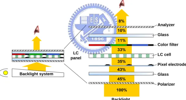
LCD requires a great deal of energy for the backlight system, as shown in Fig. 1-1.
LC panel Backlight system Analyzer Glass Color filter LC cell Pixel electrode Glass Polarizer Backlight
Fig. 1-1. A transmissive type LCD with backlight system and the light transmittance after light passes through each component of the LCD.
Besides, the devices in the LCD embodiment including polarizer, pixel electrode, LC cell, color filter, and analyzer absorbs or blocks the backlight, so that the transmittance is only about 8%. Therefore, such low light throughput requires a powerful backlight system to achieve sufficient brightness, thus inefficient in energy
usage. Consequently the applications that utilize this technology, like notebooks, have great concern on battery. Moreover, the optical properties of the LC material and the polarizer also causes the “viewing angle effect”.
1.2 Organic Light Emitting Device as a Promising Alternative
With these remain issues of LCD’s, there has been a lot of effort to find alternatives for display applications. Since the report of high efficiency
electro-luminescence from organic light-emitting device in 1987 by Tang et. al [2],
OLED has raised a great interest among the display community. Later, Burroughes et. al. demonstrated that a conductive organic polymer film consisting of poly paraphenylenevinylene, or PPV, can be used as the active element in a large-area light
emitting device [3]. As a relatively new technology, OLED uses thin layers of organic
small molecules or polymers whose behaviors are much like single-crystal semiconductors. A light-emitting layer sandwiched between an electron-transport and a hole-transport layer can act much like a conventional LED with electrons and holes combining in the emitting layer to produce light. Unlike LCD’s, the OLED is self-emissive thin-film device that requires neither the backlight, top glass, nor the color filter. Color can be achieved either through selective doping of the organic small molecules or through alternating the organic polymer structures. OLED-based displays have the potential of being lighter, thinner, brighter and much more power-efficient than LCD. Moreover, OLED-based displays do not suffer from the viewing angle issues. There are several important features for OLED as display applications.
1. In organic devices the materials are usually fabricated as thin amorphous films, which can be processed easily over large areas;
2. Amounts of organic materials are relatively small (100 nm thick) in the display fabrication process so that large-scale production (chemistry) is easier than for inorganic materials (growth processes of single crystals etc.);
3. OLED can be tuned chemically in order to adjust the band gap separately, charge transport as well as solubility and several other structural properties; 4. The amorphous nature of polymers provides additional advantages in terms of
film fabrication;
Recent improvements in the quantum efficiency of OLED have given a much needed
boost to the several key applications [4]. A complete overview of several techniques to
improve the resolution and brightness of these displays can be found in these works
[5][6][7]
. In the future, OLED displays are likely to compete with LCD’s in applications ranging from cellular phone displays to high information content notebook computers due to its unique features.
1.3 Polysilicon TFTs for active-matrix addressing
During the past few decades, the passive-matrix addressing technology for either LCD or OLED was optimized to achieve the maximum performance. However, the contrast ratio of passive-matrix addressing is limited because the duration of pulsed signal decreases as the display resolution and gray level increase. Passive-matrix addressing has been replaced by active-matrix addressing in high-information content applications. Active-matrix arrays contain many individual elements commonly known as pixels, which are generally addressed or read out by a grid structure of interconnecting lines termed gate and data lines. In active-matrix array, each pixel is usually composed by either two-terminal or three-terminal devices which work as a switch to store and retain the video information on a storage capacitor during a
complete frame time. The two-terminal device, typically a Schottky or PIN diode that passes current one way, is usually made of amorphous silicon, a bidirectional current-passing metal-insulator-metal (MIM) structure with an insulator film
composed of PECVD-deposited silicon nitride (SiNx), diamond-like carbon, or
tantalum pentoxide (Ta2O5) [8][9][10]. The three-terminal array switches are field-effect
transistors (FETs), such as crystalline Si (c-Si) metal oxide-semiconductor field-effect transistors (MOSFETs) or thin-film transistors (TFTs). Since the lithography-stitching limits, large area c-Si manufacturing is still very costly, and the temperature required for bulk crystalline formation make it difficult to integrate c-Si with plastic or glass substrates. Therefore the c-Si active-matrix arrays are only restricted to small size (< 1
in.2), high-resolution displays, such as head-mounted displays and light valves
commonly used in projection displays. By contrast, the thin-film transistors can be easily fabricated for large size substrate by either amorphous or polycrystalline silicon technologies.
Hydrogenated amorphous-silicon (a-Si:H) is used extensively to fabricate TFTs for flat-panel displays. a-Si:H TFTs have a low leakage current and sufficient on-current for most applications, and can be fabricated at low temperatures (< 350ºC) on inexpensive glass substrate. However, a-Si:H TFTs suffer from poor carrier mobility and large threshold voltage shift. The mobility of amorphous-silicon is too
low (0.1~1 cm2/V-s) to be used in the peripheral driving circuitry, so that
single-crystal integrated circuitry must be bonded to a substrate containing the amorphous-silicon active matrix, consequently, increasing the cost and decreasing the reliability. Besides, the low mobility also causes a limitation on the aperture ratio and the pixel size for display applications, and the poor hole mobility prohibits a usable p-channel TFT. The drifting threshold voltage also imposes reliably in integrated
display drivers, such like column multiplexer and the shift register circuits of scan line.
Polycrystalline silicon (poly-Si) TFT technology presents advantages over a-Si technology on the achievable size-versus-resolution limits for the display, as well as the opportunity to integrate additional functionalities on the panel. The advantages of poly-Si technology primarily originate from the significant performance of poly-Si TFT and the fabrication compatibility with CMOS technology which is capable to monolithically integrate peripheral drivers on the panel. Essentially, the effective
carrier mobility in poly-Si of 10~500 cm2/V-s is significantly higher than that of a-Si.
The higher mobility can:
Reduce the size of the TFT and increase aperture ratio resulting in higher brightness and lower power. The higher mobility enables smaller channel widths to be used for a given channel length while retaining sufficient driving current. Higher aperture ratio is also achieved through full self alignment of the source/drain regions which can reduce the parasitic and overlap capacitance and the size of the storage capacitor.
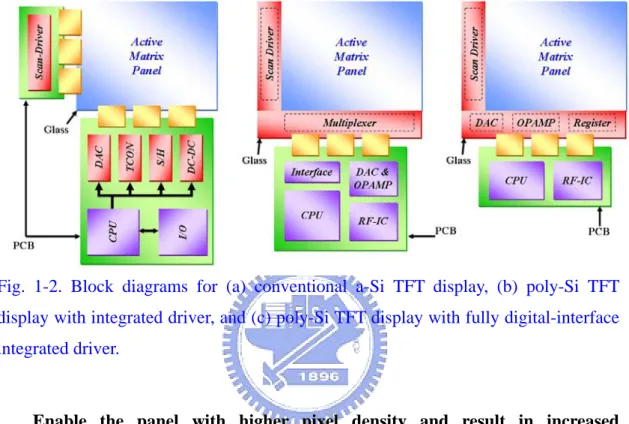
Enable the integration of driver and the possibility of a complete system on glass and increase the panel reliability. The ability of poly-Si TFT to integrate driver circuitry on active-matrix display panels can lead to more reliable displays. Driver integration not only eliminates the weight and thickness of the display module, but also reduces a number of driver ICs and the interconnections between the display panel and the external print circuit boards (PCBs) so that the display module can significantly withstand the greater shock and vibration. Driver integration can be matched to an analog display interface or to a fully digital display interface. In the former case, key circuitries such as buffers, shift
registers, and scan driver are required. In the last case, the digital-to-analog converter (DAC), operational amplifier (OPAMP) and high speed register are
needed, in addition to the components for the analog interface, as shown in Fig.
1-2.
Fig. 1-2. Block diagrams for (a) conventional a-Si TFT display, (b) poly-Si TFT display with integrated driver, and (c) poly-Si TFT display with fully digital-interface integrated driver.
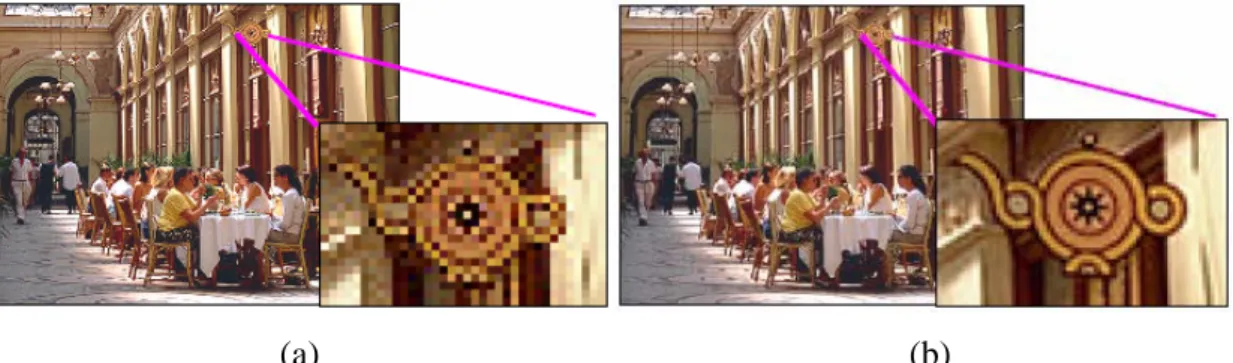
Enable the panel with higher pixel density and result in increased information content and legibility. The smaller transistors and reduced TFT “ON” resistance result in a reduced resistance capacitance (RC) delay which allows more pixels to be squeezed on a given display and while still satisfying the programming time, power consumption, and luminance requirements. The time required to settle a pixel to the required voltage accuracy to achieve the desired gray level is called the programming time which is a function of RC delay. Poly-Si TFT has a lower RC delay so that the multiplexed addressing scheme for high resolution display is easily achieved. In a-Si TFT technology, as the resolution increases with the fixed mobility and channel length, a larger TFT and high operation voltage are needed to charge the pixel in an available time,
therefore, result in the reduced aperture ratio, lower luminance and high power consumption. Consequently, poly-Si TFT is a better candidate to achieve smaller pixel pitch and higher pixel density to meeting the requirements of high
resolution display, as shown in Fig. 1-3.
(a) (b)
Fig. 1-3. Picture quality resolution for active-matrix displays achieved by (a) a-Si TFT and (b) poly-Si TFT technologies.
1.3.1 Mobility
The effective velocity of carriers through a given material is the product of the
mobility which is termed µn (electron mobility) and µp (hole mobility) and the electric
field strength. In semiconductor theory, the drain current of TFT is proportional to mobility. To achieve a given current, the higher mobility the TFT possesses, the
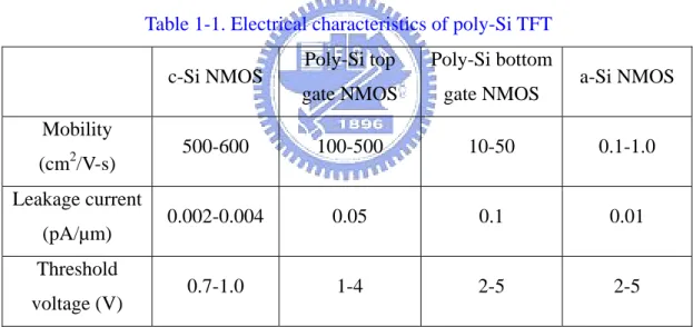
smaller the transistor width to length ratio (W/L) can be employed. As shown in Table
1-1, mobility for c-Si semiconductor devices is in the range of 500 to 600 cm2/V-s,
while poly-Si TFT mobility ranges from 100-500 cm2/V-s for top gate NMOS devices
and 10-50 cm2/V-s for bottom gate NMOS devices. In the case of a-Si TFT, mobility
is typically 0.1-1 cm2/V-s. Because top gate device with fully aligned source and drain
regions results in significantly higher mobility performance, it has been adopted for most poly-Si TFT fabrications.
performance is closely related to the grain size. C-Si, with a single grain has the highest mobility among the mentioned fabrication technologies. In poly-Si the nature of the crystallization process typically results in the formation of numerous small grains under 1µm which reduces the mobility. Because there are typically numerous grains in the channel, the uniformity of the grain size is also critical. A great deal of researches have studied the variations in laser energy density as the cause of grain size non-uniformity problems. Thus, despite the mobility of poly-Si today is at the lower end of the range, it is expected to be improved in the near future if larger grain size with controlled grain boundaries are implemented which will shorten the performance gap with c-Si devices.
Table 1-1. Electrical characteristics of poly-Si TFT
c-Si NMOS Poly-Si top
gate NMOS
Poly-Si bottom
gate NMOS a-Si NMOS
Mobility (cm2/V-s) 500-600 100-500 10-50 0.1-1.0 Leakage current (pA/µm) 0.002-0.004 0.05 0.1 0.01 Threshold voltage (V) 0.7-1.0 1-4 2-5 2-5
1.3.2 Leakage current
A low “OFF” current , IOFF, or called leakage current is essential for good pixel
voltage retention. Leakage current has been a serious issue for poly-Si TFT active-matrix array and manifests itself in the form of image degradation. Poly-Si leakage current is typically 5-10 times larger than that of a-Si and 25-50 times larger
caused by grain boundaries in the high electric field region between the drain and the gate edge. Based on the nature of the device structure, leakage current is typically larger for bottom gate devices than that of top gate devices. To reduce the leakage current, it is necessary to suppress the electric field density in the channel at the edge of the drain. The reduced electric field density not only suppresses leakage current when the gate and drain are biased, but prevents degradation of device characteristics over time due to the injection of “hot” electrons into gate oxide. Numerous methods have been proposed for reducing the leakage current, for example, adopting a single or double lightly doped drain (LDD) or implementing multiple gates. An LDD can reduce the high gate-to-grain field and the multiple gates can decrease the probability of grain boundaries occurring at the drain edge.
1.3.3 Threshold voltage
Threshold voltage (Vth) is the value of gate-to-souce voltage (VGS) at which a
sufficient number of mobile electrons accumulate in the channel region to form a
conduction region. Vth is of positive value for an n-channel device and negative for a
p-channel device. The value of Vth is controlled during device fabrication and is of
less than 1V for c-Si devices as shown inTable 1-1. The drain-to-source voltage (VDS)
causes a current to flow through the induced channel. The current is carried by free electrons traveling from the source to drain. The magnitude of the drain current
depends on the density of electrons in the channel, which depends on VGS. When
VGS=Vth, the channel is nearly induced and the current is negligibly small. As VGS
exceeds Vth, more electrons are attracted into the channel and the conductance of the
channel is proportional to the overdrive gate voltage (VGS-Vth). Since threshold
will operate at a higher Vth and require higher source voltage, implying greater power
consumption.
1.3.4 Poly-Si TFT fabrication flow
As already discussed, a key advantage of poly-Si TFT technology is the ability to integrate the driver circuitries with the pixel array on the same substrate. The following illustration shows a representative process flow for the simultaneous fabrication of n- and p-channel TFTs which are compatible with conventional CMOS process. This particular process flow yields self-aligned, top-gate poly-Si TFT with the LDD configuration. The process is outlined next and shown schematically from
Fig. 1-4(a)to Fig. 1-4(l).
Typical process flow for self-aligned top-gate poly-Si TFT
1. Sequential deposition of base coat (SiO2, SiNx) and a-Si film on the glass
substrate.
2. a-Si de-hydrogenation
3. Low-temperature crystallization of a-Si film with excimer laser to obtain poly-Si film.
4. Mask #1: active island definition, Fig. 1-4(a).
5. Mask #2: Channel doping for n-channel TFT, Fig. 1-4(b).
6. Mask #3: Source/Drain (S/D) region doping, Fig. 1-4(c).
7. Deposition of gate dielectric layer, Fig. 1-4(d).
8. Gate metal deposition
9. Mask #4: Gate definition, Fig. 1-4(e).
10. LDD region doping with self-aligned structure, Fig. 1-4(e).
12. Deposition of interlayer dielectric film, Fig. 1-4(g).
13. Mask #6: S/D contact hole definition, Fig. 1-4(h).
14. S/D metal deposition.
15. Mask #7: S/D electrode definition, Fig. 1-4(i).
16. Deposition of organic planarization layer, Fig. 1-4(j).
17. Mask #8: ITO electrode contact hole definition, Fig. 1-4(k).
18. Pixel ITO deposition.
19. Mask #9: ITO electrode definition, Fig. 1-4(l).
a-Si SiO2 SiNX
N-ch P-ch B+ Resist Channel Doping N-ch P-ch (a) (b) PHx+ N+ Doping N-ch P-ch SiNX SiO2 N-ch P-ch (c) (d) PHx+ LDD Doping N-ch P-ch B2Hx+ N-ch P-ch P+ Doping (e) (f)
SiNX SiO2 N-ch P-ch N-ch P-ch (g) (h) N-ch P-ch N-ch P-ch (i) (j) N-ch P-ch N-ch P-ch (k) (l)
Fig. 1-4. Process flow of self-aligned top-gate poly-Si TFT with lightly doped drain configuration. (a) Deposition of a-Si and buffer layere (SiOx and SiNx). (b) Channel doping for N-channel TFT. (c) Source/drain doping for N-channel TFT. (d) Gate oxide deposition. (e) LDD doping with self-alignment structure. (f) Source/drain doping for P-channel TFT. (g) Deposition of insulation layers. (h) Contact hole etching. (i) Metal electrode deposition. (j) Organic preservation layer deposition. (k) Contact hole etching and (l) ITO electrode depositon.
1.4 OLED combined with poly-Si TFT
in higher brightness. In the case of a-Si TFT, a device with larger W/L and higher operation voltage are essential to provide enough current supply to the OLED. Nonetheless, larger W/L TFT design results in less OLED emission, which means smaller aperture ratio in the bottom emission structure AM-OLED. Because a pixel consists of TFT area and OLED emitting area, the larger the occupation area of TFT, the smaller the OLED emitting area. As the resolution gets higher, pixel size becomes smaller but the area of TFT remains the same. Hence, the OLED emitting area becomes smaller, prohibiting the a-Si TFT to be used in small sizes with very high-resolution AM-OLED applications. Therefore, the motivation for the integration of OLED and poly-Si TFT technology is desired to give a power-efficient operation and increase the reliability of the panel. This is due to the high drive currents and the long term stability of the poly-Si TFT compared to the a-Si TFT, while a sufficient
current supply from TFT is essential for panel operation [11][12][13].
Nonetheless, even poly-Si technology offers the potential of great driving capability and driver circuitry integration, the AM-OLED design still has several technical challenges:
Poly-Si TFT Vth uniformity - Poly-Si TFT threshold voltage uniformity is
primarily a function of the laser annealing process stability. The uniformity variance should be of less than 5% across the panel to allow for adequate margins in designing the proper gate and data voltages. When the uniformity exceeds the design margins, the potential for not fully charging the pixel exists. That will result in uneven brightness for a give gray level. Compensating for non-uniformity by increasing voltage inversely increases the power consumption.
Lifetime - It was already known that a high drain voltage and a relatively high gate voltage (hot-carrier conditions) in poly-Si TFT can decrease the maximum
transconductance and causes the variation of threshold voltage [14][15][16][17]. The degradation of transconductance and the threshold voltage variation associating with bias and temperature stress are of great concern to integrate TFTs on the substrate. Besides, the degradation alters the characteristics of poly-Si TFTs in pixel electrode circuitry so that the output current for driving OLED deviates with given voltage signals as well. In other words, the variation of display luminance accompanied with device degradation results in image quality degradation.
1.5 Motivation and objective of this dissertation
New generation mobile communication and personal information systems, such as mobile phone, hand-held personal computer (HPC), digital camera, and game-boy player have progressed rapidly. Displays with the features of light weight, low power, bright, wide viewing-angle, and full color are essential for above applications. OLED combined with poly-Si TFT technology to form an AM-OLED is an unique feature those requirements. However, the AM-OLED still has several issues needed to be improved.
This dissertation presents a detailed study of the design of pixel electrode and integrated driver circuitries to improve the image quality and functionality testability for AM-OLED based on poly-Si TFT technology. The theoretical analysis of the performance of pixel electrode circuit and integrated driver circuitries will base on the principle of poly-Si TFT. Additionally, the 9-masks fabrication process for poly-Si TFT was utilized to realize the design.
Since the luminance of OLED is directly proportional to the driving current, each pixel in active-matrix TFT array consumes a certain amount of current supplied by the power electrode. The power electrode in active-matrix array is usually fabricated by
metal materials such as molybdenum (Mo), aluminum (Al) and copper (Cu). The current signal passing through these metal wires can generate the voltage drop due to the intrinsic resistance and affect the luminance uniformity. Increasing the wire width of the electrode can reduce the parasitic resistance, however, the aperture ratio will be decreased. It is expected that the voltage drop caused by the parasitic resistance will become the critical drawback in display applications of large size and high resolution. In this dissertation, we propose a simple AC voltage driving scheme with an adequate design of conventional two transistors (2-T) pixel circuit for AM-OLED displays. By means of the charge feed-through mechanism of storage capacitor, the proposed AC driving scheme can counteract the voltage drop caused by the parasitic resistance. Without employing the complicated driving system, the AC driving scheme can effectively improve the brightness uniformity.
Ensuring the brightness uniformity of each pixel is essential for rendering of high quality images of poly-Si TFT AM-OLED. The variations of device characteristics caused by device aging or manufacturing process are still an issue in poly-Si TFT technology. More specifically, the variations of threshold voltage can affect the drain current and lead to change of the pixel luminance. Due to the variation of device characteristics, the current driving technology with self-compensation function is the leading scheme for achieving the uniform image quality for AM-OLED. In this research, we proposed a fully-integrated current-type driving system including the pixel electrode circuitry, current generator, current-type DAC, and current-type memory. With this integrated driver, only small digital voltage signals are needed for the display interface so that the conventional driver ICs for active-matrix display still can be used. Besides, the precise current signal for various gray levels can be correctly manipulated in this driver system to compensate the characteristic variations
of poly-Si TFT.
In active-matrix TFT array processes for both AM-LCD and AM-OLED applications, TFT array inspection and yield management are important to ensure the reliability of display applications. In-line testing of TFT array in a manufacturing process is beneficial for yield improvement because the faulty TFT array can be repaired or scrapped before encapsulation, and external driver assembly. Likewise, utilizing TFT array testing for failure analysis can detect the location of the faults and identify the categories of faults in TFT array. The conventional AM-OLED pixel circuit does not provide for fully functional testing with electrical charge sensing scheme as the AM-LCD pixel does, unless an additional component can be added-in. Here, we propose the modified pixel circuit for not only the voltage-driven but also the current-driven pixel circuitries to measure the characteristics of TFT and detect defects. The convenient charge sensing scheme can be used to effectively determine and analyze the circuit breaks, shorts, and leaky transistors or capacitances. The proposed TFT array testing scheme is demonstrated to be a good tool for managing the yield of the array process of AMOLED.
1.6 Organization of this dissertation
The dissertation is organized as following: The review of OLED technology is presented in Chapter 2. The physical mechanism, fabrication process, full-color technologies and lifetime issues are described in this chapter. In Chapter 3, the basic analysis of passive-matrix addressing scheme is described to derive the limitation of PM-OLED. Following is the fundamental design principle of conventional voltage-driven AM-OLED. To suppress the issues of conventional voltage-driven AM-OLED due to the parasitic resistance effect, AC driving scheme, which can yield
high luminance uniformity and long device lifetime, is shown in Chapter 4. Due to inherent characteristics variations of poly-Si TFT that result in inferior luminance uniformity, using current-driven scheme with full-integrated driver circuitries for enhancing the image uniformity are demonstrated in Chapter 5. In this chapter, different designs of pixel circuit are detailed to improve the long programming time issue induced by current-driven scheme. Moreover, the design for peripheral driver system including current-type DAC, and high-speed current memory are also described. An modified current-driven pixel electrode circuit with current scaling function which can enhance the data programming speed is discussed in Chapter 6. In Chapter 7, the charge-sensing approach with the modified pixel schematic is presented to easily enhance the functionality testability of AM-OLED. Finally, discussions and summary of this dissertation, and recommendations for the future works are given in Chapter 8.
Reference
1. A. J. Snell, K. D. Mackenzie, W. E. Spear, P. G. LeComber, and A. J. Hughes, “Application of amorphous silicon field effect transistors in addressable liquid crystal display panels,” Appl. Phys., vol. 24, pp. 357, 1981.
2. C.W. Tang and S. Van Slyke, “Organic electroluminescent diodes”, Appl. Phys. Lett., vol. 51, pp. 913, 1987.
3. J. H. Burroughes, D. D. C. Bradley, A. R. Brown, R. N. Marks, K. Mackay, R. H. Friend, P. L. Burns, A. B. Holmes, “Light emitting diodes based on conjugated polymers,” Nature, vol. 347, pp. 539, 1990.
4. W. Lai, P. Ng, M. C. Y. Chan, W. Chan, E. H. Li, “Improved external efficiency of light emitting diode using organic thin film,” in Tech. Dig. CLEO/Pacific Rim 1999, pp. 246. 5. Y. Kijima, N. Asai, N. Kishii, and S. Tamura, “RGB luminescence from passive-matrix organic LED’s,” IEEE Trans. Elec. Dev., vol. 44, pp.1222, Aug. 1997.
6 . T. Tohma, “Recent progress in development of organic electroluminescent display devices,” in Int. Display Research Conference Dig. Tech. Papers, 1997, F1.1.
7. S. R. Forrest, “Active optoelectronics using thin-film organic semiconductors,” IEEE J. Sel. Top. Quant. Elec., vol. 6, no. 6, pp. 1072 , Nov.-Dec. 2000.
8. H. F. Cheng and I. N. Lin, "Ferroelectric MIM and MOS structure of laser deposited (Sr0.2Ba0.8) TiO3 thin films ", in Proc. 9th IEEE Int'l Symp. Appl. of Ferroelectrics, 1994, pp.59.
9. E. Ohta, Y. Kimura, H. Kndo, M. Takahashi, K. Kameyama, K. Yamada, and I. Fujimura, “MIM switching devices using diamond-like-carbon films,” IEEE Trans. Elec. Dev., ED-21, pp. 146, 1974.
10. R. A. Hartman, “Two-terminal-device addressed LCD,” in Symp. Dig. 1995 SID, 1995, pp. 7.
11. G.. Rajeswaran, M. Itoh, S. Barry, T. K. Hatwar, K. B. Kahen, K. Yoneda, R. Yokoyama, T. Fukuda, N. Komiya, H. Kanno and H. Takahashi, “Active-matrix low-temperature poly-Si TFT/OLED full-Color displays: status of development & commercialization,” in Symp. Dig. 2000 SID, 2000, pp. 974.
12 . Z. Meng, H. S. Kwok, and M. Wong, “Metal-Induced unilaterally crystallized polycrystalline silicon thin-film transistor technology for active-matrix organic light-emitting diode displays with reduced susceptibility to cross-talk,” in Symp. Dig. 2002 SID, 2002, pp. 976.
13. T. Sasaoka, M. Sekiya, A. Yumoto, J. Yamada, T. Hirano, Y. Iwase, T. Yamada, T. Ishibashi, T. Mori, M. Asano, S. Tamura, T. Urabe, “A 13.0-inch AM-OLED display with top emitting structure and adaptive current mode programmed pixel circuit (TAC),” in Symp. Dig. 2001 SID, 2001, pp. 384.
14. G. Fortunato, A. Pecora, G. Tallarida, L. Mariucci, C. Reita, P. Migliorato, “Hot carrier effects in n-channel polycrystalline thin-film transistors: A correlation between off-current and
transconductance variations,” IEEE Trans. Elect. Dev., vol. 41, pp. 340, Mar. 1994.
15. I.-W. Wu, W. B. Jackson, T. Y. Huang, A. G. Lewis, A. Chiang, “Mechanism of device degradation in n- and p-channel polysilicon TFT’s by electrical stressing,” IEEE Elec. Dev. Lett., vol. 11, pp. 167, Jan. 1990.
16. F. V. Farmakis, C. A. Dimitriadis, J. Brini, G. Kamarinos, V. K. Gueorguiev, T. T. E. Ivanov, “Hot-carrier phenomena in high temperature processed undoped-hydrogenated n-channel polysilicon thin film transistors (TFT’s),” Solid-State Elec., vol. 43, pp. 1259, 1999. 17. M. Hack, A. G. Lewis, and I.-W. Wu, “Physical models for degradation effects in polysilicon thin-film transistors,” IEEE Trans. Elec. Dev., vol. 40, pp. 890, May 1993.
Chapter 2
OLED - Organic Light Emitting Device
2.1 Introduction
During the last fifty years, the semiconductor physics have played an important role in industrial and technical developments and are used in numerous applications, e.g. diodes, transistors and sensors. Compound materials with combinations of the III– and V-groups of periodic system possess semiconductor properties. The principle of light generated by applying an electrical field to this semiconductor material is known as electroluminescence. A conventional LED constructed of semiconductor materials is based on this luminescence phenomenon and has been mass-produced in the last thirty years. The applications for the LED are found in several areas including optical communication and dot matrix displays because of their ability to emit intensive light.
In spite of the fact that the organic material carbon (C) is positioned in the IV-group as the semiconductors materials, it is considered as an isolator. Nevertheless, Hideki Shirakawa discovered a conducting ability of the organic material in 1977
[1][2][3][4]
for his the Nobel Prize in chemistry in 2000 and started a new era of the semiconductor technology for new applications.
In 1987, the group of Tang and Van Slyke at Eastman-Kodak presented
luminescence by an organic material [5]. The group constructed an efficient OLED,
which was driven by a rather small voltage. The technique they used to emit light was vacuum deposition of small molecules to form a multi-layer thin-film structure. The layered structure is sandwiched between two electrodes: anode and cathode. The thin layer (<1 µm) of organic material permits a high electrical field at low voltage. Thus,
light from thin film organic materials is usually produced at low voltage. High quality thin molecular layers were an important condition for the development of OLED.
In 1990, a group at the Cavendish Laboratories at Cambridge University presented the first LED using polymers as active material. The active polymer was a
conjugated polymer [6]. In comparison to the traditional solid state LED, the new
organic approaches were believed to be much more efficient. The conjugated polymers and small molecules are considered as the two classes for OLED. The two classifications of light-emitting organic layers in the OLED devices both possess luminescent and conductive properties. Small molecules have molecular structures of relatively short chain length and consequently low molecular weights. The most commonly used material with the most explored properties among the small
molecules is tris-(8-hydroxyquiniline) aluminum (Alq3), as shown in Fig. 2-1(a). The
conjugated polymers are composed of a long repeating chain of similar smaller molecules, called monomers. They possess consequently, compared to small molecules, a molecular weight twenty to fifty times higher. A frequently used
conjugated polymer is the poly-paraphenylene vinylene (PPV), as shown in Fig.
2-1(b).
(a) (b)
Fig. 2-1. Chemical structures of (a) tris-(8-hydroxyquiniline) aluminum (Alq3) and (b)
2.2 Luminescence of organic materials
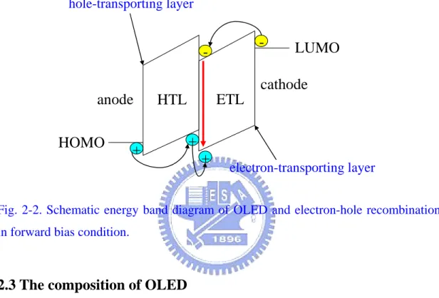
Organic materials refer to a base of the IV-group carbon and with additional elements such as hydrogen (H), nitrogen (N), oxygen (O), phosphorus (P) and sulfur (S). Since polymers and organic materials are not referred to conducting materials because of the large band gap between conduction and valence bands, a very high electrical field has to be applied. When applying an electrical field, charge carriers including hole and electron are injected from the electrodes into the organic layer respectively and result in geometrical defects on the symmetric organic structure and exhibit a lower band gap according to
Fig. 2-2. The charged carriers move along the structure and the attraction between the carriers results in a recombination of electron and hole to form an exciton which has a possibility to emit light as photons. The exciton is either in singlet or in
triplet-state according to the Pauli’s principle [7]. The exciton will form two new
energy bands inside the band gap. The energy level of the exciton is below the conduction band and the released energy is emitted as photons. Upon the relaxation of exciton, heat and photons will be emitted with an energy set according to the gap between the energy bands. The states of the exciton have certain influence of the emission of light and quantum efficiency since the singlet states release its energy as an emission of photons. However the triplet-state is regarded as the heat forming state and can not transfer to light. In some special cases, the triplet-state generates light as well.
The backbone of the organic materials is strongly localized bonds between the carbon atoms. The conductivity is enabled through bonds that are orthogonal to the backbone. The length of the conjugation, i.e. the conjugation length, set certain characteristics of the molecule. The conjugation length defines the length where the
electron is free to move within. In general, small molecules tend to have short conjugation length, while longer conjugated molecules, polymers, may have a longer. Longer conjugation length results in a smaller band gap. It is therefore easier to produce red light with conjugated polymers compared to small molecules, and consequently small molecules can more easily generate blue light.
cathode
anode
+
-
-+
+
hole-transporting layer electron-transporting layerHTL
ETL
HOMO
LUMO
Fig. 2-2. Schematic energy band diagram of OLED and electron-hole recombination in forward bias condition.
2.3 The composition of OLED
2.3.1 The mono-layer device
The simplest OLED, a mono-layer device, is constructed of a thin layer of
organic material sandwiched between two electrodes. As shown in Fig. 2-3(a), the
function of the anode is to supply positively charged holes and a frequently used material, due to the requirement of transparency, is the Indium Tin Oxide (ITO). The cathode electrode supplies electrons to the organic layers. The charged carriers of electrons and holes are injected into the thin emitting layer material where they form an exciton and generate photons afterwards. The fact of the singlet and triplet states of the excitons has a certain influence and limitation on the device quantum efficiency.
Because of the disordered structure in organic materials, the behaviors of the charged carriers in organic materials are not similar to that in metal. This fact impedes
a recombination and decreases its probability [8]. Therefore, there is always one
dominant charge carrier that moves through the material without recombining with the opposite charge carrier. Another problem related to mono-layer devices is that the charge carriers tend to remain at one of the electrodes and creating space charges that prevent further hole and electron injections. Furthermore, if charges form an exciton near a metal, quenching mechanism can destroy the exciton and reduce the light generation efficiency. + + + + + - - - - -glass anode cathode emitting layer + glass anode cathode emitting layer + + + + -ETL (a) (b)
Fig. 2-3. Configurations of OLED for (a) fundamental single-layer structure and (b) double-layer heterostructure structure.
2.3.2 The double-layer device
A minimization of the energy barrier between the electrodes and the organic material is another approach to enhance the injection of the carriers. The mono-layer device is then upgraded to a double-layer device. Instead of one organic layer, two layers, an emission and an electron-injection layer, are placed between the electrodes,
as shown in Fig. 2-3(b). By choosing the materials according to their properties of
manner into the emission zone where an emission of light takes place [9].
The band diagram of the materials can be matched better to the specific electrodes through the double-layer construction and result in improved equilibrium of the currents of holes and electrons. The electrical field can consequently be decreased, which increases the efficiency and lifetime of the device. The difference in energy levels between the two organic layers creates a potential barrier at the interface. The barrier confines the holes and electrons and contributes to an increased
recombination probability [10].
2.3.3 The multi-layer device
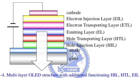
The functionality of the double-layer device and its components can be further improved with regard to several layers and minimal potential barriers. The greatest advantage of a multi-layer structure, compared to a double-layer, is the possibility to separate transport regions from the emitting region. This multi-layer structure accomplishes a better performance and an increased range of colors of the emitted light. By tuning the voltage over the electrodes, a proper placement of the emitting zone can be achieved, which may improve the efficiency of the device. The structure in Fig. 2-4 is an example of a multi-layer bottom-emission OLED, which has its light emitted through the transparent anode.
The substrate on which the OLED is fabricated consists of a material with a rigid or a flexible structure, e.g. glass or plastics. Compared to flexible substrates, rigid materials are of advantage for their ability to prevent the device from moisture and air. An outer exposure of moisture and air without any protection significantly degrades the lifetime and performance of the device.
layer (HIL) is introduced for control and an enhancement of the injection of the holes into the hole transport layer (HTL). An effective HTL of p-type material can effectively enhance the transportation of holes to the emitting zone. The excitons are expected to be formed in the emitting layer (EL) and eventually emit light. Since equilibrium of mobilities between the carriers is difficult to achieve, a blocking layer can be used to confine the charge carriers to perform a maximum recombination.
glass anode
Emitting Layer (EL)
Hole Transporting Layer (HTL) Hole Injection Layer (HIL) Electron Injection Layer (EIL) Electron Transporting Layer (ETL) cathode
Fig. 2-4. Multi-layer OLED structure with additional functioning HIL, HTL, EIL and ETL.
The electron transport layer (ETL) is of n-type doped material which can enhance the mobility of the charge carriers and the transportation of electrons to the emitting layer. The layer also functions as hole blocking and is suitable to control specific charged carries. The ETL can, similar to the HTL, be used as an emitting layer. Similar to the holes, an organic electron injection layer (EIL) is used to assist the electrons to cross the barrier between the cathode and the ETL. Due to the enhanced transportation of electrons, a low electrical field is adequate for the multi-layer device and leads to a more power efficient OLED. It is furthermore possible to use the same material for the two electrodes, yet at a reduced efficiency.