國 立 交 通 大 學
電子工程學系電子研究所
博 士 論 文
射頻CMOS主動電感器的研究與應用
The Study of Radio Frequency CMOS Active
Inductors and Applications
研 究 生 :楊 鎮 澤
指導教授 :李 鎮 宜
射頻CMOS主動電感器的研究與應用
The Study of Radio Frequency CMOS Active Inductors
and Applications
研 究 生:楊 鎮 澤 Student :Jenn-Tzer Yang
指導教授:李 鎮 宜 博士 Advisor :Dr. Chen-Yi Lee
國立交通大學
電子工程學系電子研究所
博士論文
A Dissertation
Submitted to Institute of Electronics
College of Electrical Engineering and Computer Science
National Chiao Tung University
in Partial Fulfillment of the Requirements
for the Degree of
Doctor of Philosophy
in
Electronics Engineering
February 2006
Hsinchu, Taiwan, Republic of China.
Acknowledgments
I would like to express my sincere appreciation to my advisor Prof. Chen-Yi Lee for his sophomore enthusiastic guidance and encouragement throughout the research, and wholeheartedly give him and his family my best wishes.
During my research, I would like to thank National Science Council (NSC) for supporting the project of My Ph. D work. The chip implementation support from Chip Implementation Center (CIC) of NSC is acknowledged, too.
I would like to thank my senior Si2 group mates, Dr. Terng-Yin Hsu and Mr. Terng-Ren Hsu for many valuable discussions and helps. Besides, I like to thank my junior Si2 group mates, Mr. Hsuan-Yu Liu and Mr. Chien-Ching Lin for their kind support. I also like to thank all the Si2 group members in NCTU for their fruitful assistance during the time of my graduate school.
Finally, I give the greatest respect and love to my children, my parents in law and my wife (Wei-Wei). I want to express my highest appreciation for their support and understanding. Except those, I would also like to express my appreciation for the thesis proofreading work done by my nephews, J.C. Hu and J.T. Hu. This thesis is dedicated to them for assisting me to achieve the most important stage in my life. I will never let them down and wish them all the successes in the future.
射頻CMOS主動電感器的研究與應用
研究生:楊鎮澤 指導教授:李鎮宜博士 國立交通大學電子工程系電子研究所摘要
在本論文中,我們首先針對各種不同的CMOS主動式電感器(Active Inductor)與負 電導產生器(Negative Conductance Generator)的組合應用於不同工作頻率的射頻放大 器設計研究,並且對各種不同的主動式電感器使用不同的損失補償技術來改進此電感器 特性的設計。接著將此改進的主動式電感器應用於寬頻放大器(Wideband Amplifier)與 電壓控制震盪器(Voltage-Controlled Oscillator)電路,以證實射頻電路中使用主動電 感器能得到比使用平面螺旋型電感器(Planar Spiral Inductor)有更好的優點。如,可 得到很高的品質因數(Quality Factor)、高的電感量(Inductance)等特性;並且使用主 動式電感器的射頻電路於晶片製作時的面積將比使用平面螺旋型電感器的射頻電路所佔 的晶片面積小很多的優點。 本論文首先描述使用平面式螺線型電感器元件應用於射頻放大器設計,雖能得到良 好的特性結果,但仍有些缺點產生。如,平面式螺線型電感器佔用的晶片面積太大、品 質因數很低、不容易準確控制電感的特性等缺點。而這些缺點可以使用主動式的電感器 來給予改善。應用目前已經存的主動電式感器結合改進電感器特性的負電導產生器技術 設計工作於不同頻帶的射頻放大器。經由模擬結果得到輸出的增益可達到17dB以上、雜 訊指數低於6dB,此結果與使用平面式螺線型電感器相近,而面積為使用平面式螺線型電感器的四分之一及使用主動電感器的功率消耗也有明顯的降低。所以,得知使用主動式 電感器將優於使用平面式螺線型電感器。 然而,為降低改善主動電感器特性的電路複雜度,提出各種不同的簡單補償電路對 各種不同的電感器作改良設計,得到高效能的主動電感器,且能得到電路非常簡單的電 感器。經由數學的分析、電路的模擬及實際的測量結果,此改良後的電感器可得到很高 的品質因數(約104 以上)。最後,將此改良後的主動式電感器應用於寬頻放大器及電壓 控制振盪器的電路中。於寬頻放大器可以得到頻帶寬度由0Hz到1GHz有平坦的增益(約 18dB)特性。對於電壓控制振盪器得到寬的調整範圍(1GHz到3GHz)、-98dBc/Hz的相位 雜訊及10mW的固定功率消耗。因此,經由以上的研究結果證實使用主動電感器於射頻電 路為一種可行的方法,此種方法可使設計射頻電路時可以大幅的降低所佔的晶片面積的 成本。
The Study of Radio Frequency CMOS Active
Inductors and Applications
Student: Jenn-Tzer Yang Advisor: Dr. Chen-Yi Lee
Department of Electronics Engineering National Chiao Tung University
Abstract
In this thesis, we will focus on the research illustration and design comparison on combing several different CMOS active inductor with negative conductance generator (NCG) applied in RF amplifier on different operating frequency. And we will apply various loss compensation techniques on several different active inductors to improve the characteristics of the inductors. Furthermore, we applied the improved active inductor on the wideband amplifier and the voltage-controlled oscillator to prove that using the active inductors in RF can have more advantages than using the planar spiral inductor. For example, the active inductor can have a higher quality factor, a higher operating frequency, and a higher inductance etc. On the other hand, in radio frequency circuit design, the size of the chip used in an active inductor will be much smaller than the one used in a planar spiral inductor.
The design of the use of the planar spiral inductor applied on the radiofrequency amplifier will be described at the beginning of the thesis. Though the above design shows the result of performing good characteristics, some disadvantages of this design also exist. For example, the size of the chip of the circuits using planar spiral inductor too large, quality factor is too low, and the characteristics of the inductor cannot be controlled easily and accurately. We presented the use of the active inductor to improve the disadvantages mentioned above. We applied the techniques of the negative conductance generator, which
combines the existing active inductor and the characteristics of the improved inductor, to work on the different bandwidth radio frequency. From the simulation results, we found that the output power gain is over 17dB, and the noise figure is lower than 6dB. The simulation also shows that the results are very close to those using the planar spiral inductor, and the size of circuit using the active inductor design is one forth of that using planar spiral inductor. Moreover, the power consumption decreases dramatically when using active inductor. So, we can conclude that using active inductor generates more benefits than using planar spiral inductor.
For minimizing the complexity of the active inductor circuits, we present several simple compensated circuits for each different active inductor to reach the goals of performing higher performance and an easy design circuit. From the mathematical analysis, simulated results, and measured results, the improved active inductor can obtain a very high quality factor, which is above 104. Finally, we present the results of applying the improved active inductor in the circuits of wideband amplifier and voltage-controlled oscillator. From the wideband amplifier’s point of view, the amplifier can generate a flat gain, which is about 18dB, in the bandwidth from 0Hz to 1GHz. From the voltage-controlled oscillator’s point of view, the voltage-controlled oscillator can generate a wide tuning range from 1GHz to 3GHz, -98dBc/Hz phase noise and steady 10mW power consumption. As the result, we can conclude that using active inductor in the radio frequency is a workable solution via the approach mention above. This solution also saves us a lot of cost taken by the size of the chip during the design stage of the radio frequency.
TABLE OF CONTENTS
Chapter 1 Introduction………..1
1.1 Motivation………...1
1.2 Thesis Organization……….….5
Chapter 2 An Overview of Active Inductors………..……….8
2.1 Design of 2.4GHz CMOS RF amplifier Using Planar spiral Inductors………..……..9
2.1.1 Circuit Design………...………..…....9
2.1.2 Simulation Results………...….…..……..10
2.1.3 Discussion………...………....…..14
2.2 Characteristics of Active Inductors………..………..….15
2.3 CMOS Active Inductors and Applications……….…………... 20
2.4 Summary………..…….…..23
Chapter 3 Designs of the RF Amplifier Using CMOS Active Inductors……….…….…..25
3.1 A 2GHz CMOS LNA with Active Inductor and Source Follower Negative Conductance Generator………..………….….…..26
3.1.1 Regulated Cascode Active Inductor………..………..……..27
3.1.2 The Source Follower Negative Conductance Generator……….……..…28
3.1.3 Low Noise Amplifier Design Methodology……….…….…….………….….29
3.1.4 Simulation Results……….……….….………….……31
3.1.5 Discussion……….…………...……….…35
3.2 A 2.4GHz CMOS Band-Pass Amplifier with High-Q Active Inductor Load……….………..…36
3.2.1 Cascode Active Inductor………...………..….………..36
3.2.3 LNA Using Q Enhancement Active Inductor Design…………..………39
3.2.4 Simulation Results………….………..….………41
3.2.5 Discussion………..………..……….45
3.3 Summary………..………...46
Chapter 4 Designs of Improving CMOS Active Inductors………..………48
4.1 An Improved Active Inductor Using a Cascode RC Feedback Compensation Technique…………..………..……….….…….49
4.1.1 Circuit Design……….………..…………...…...……..50
4.1.2 Simulation Results……….……..……….…52
4.1.3 Measurement Results……….………...………...56
4.1.4 Discussion………..………...………..…...…...……60
4.2 An Improving Active Inductor Using Gain-Boosting and Current-Reused Technique……..………..………...61
4.2.1 Circuit Design………...……..…………..61
4.2.2 Simulation Results………..…..………66
4.2.3 Discussion………..……..………….……69
4.3 Loss Compensation in RF CMOS Active Inductor Using a Capacitor…….….……69
4.3.1 Circuit Design………...………..……….………….70
4.3.2 Simulation Results………..…………....………..75
4.3.3 Discussion………...………..………79
4.4 An Improving Active Inductor Using a Resistor……….…...………80
4.4.1 Circuit Design………..……….………..…..81
4.4.2 Simulation Results………..……….…….…………85
4.4.3 Discussion………...…………...…...88
Chapter 5 Applications Based on Improved CMOS Active Inductors………...………..89
5.1 Wideband Amplifier Based on Improved Active Inductor Using a Cascode RC Feedback Compensation Technique……….…….……..…………..90
5.1.1 Wideband Amplifier with Conventional Cascode Active Inductor……..…...92
5.1.2 Improved High-Q Active Inductor Design………...…….….98
5.1.3 Wideband Amplifier with Improved Active Inductor…………..…..………101
5.1.4 Simulation Results………..103
5.1.5 Measurement Results………….……….107
5.1.6 Discussion……….………..…..…………..113
5.2 LC Oscillator Based on Improved Active Inductor Using a Resistor……..………114
5.2.1 Improved High-Q Active Inductor Design………….………….…..……….116
5.2.2 Oscillator Circuit Design……….…..……….…120
5.2.3 Simulation Results……….…...………..123
5.2.4 Discussion………..……..……….…..124
5.3 Summary………..……….127
Chapter 6 Conclusion and Future Works………..……….128
LIST OF FIGURES
Fig. 2.1 Low noise amplifier using planar spiral inductors……….…..10
Fig. 2.2 Forward Gain S21 of LNA……….……..11
Fig. 2.3 Noise Figure (NF)……….……....11
Fig. 2.4 S-parameter (S11, S22)……….………...………..…...….12
Fig. 2.5 The response of IIP3………..……….……..12
Fig. 2.6 1dB compression………....………..13
Fig. 2.7 Layout of proposed LNA ………...…… ………...……13
Fig. 2.8 Gyrator topology………..………...……..16
Fig. 2.9 A simple gyrator in MOS implementation……….………..16
Fig. 2.10 A small-signal model of the MOS transistor………..……...……….17
Fig. 2.11 Equivalent RLC model of active inductor………..………18
Fig. 2.12 The equivalent circuit of inductor……….……….19
Fig. 2.13 CG-CS configuration active inductor………..………...20
Fig. 2.14 Gain boosting compensated active inductor………..……….21
Fig. 2.15 Current-reused compensated active inductor……….………21
Fig. 2.16 Double feedback compensated active inductor……….……….22
Fig. 2.17 Negative impedance compensated active inductor…………..………...22
Fig. 2.18 Low voltage active inductor……….………..23
Fig. 3.1 Regulated cascode active inductor……….………..27
Fig. 3.2 Equivalent RLC model of active inductor………..………..27
Fig. 3.3 The negative conductance generator……….………...29
Fig. 3.4 The proposed low noise amplifier……….………...30
Fig. 3.6 S22 and S12 of the low noise amplifier……..……….…………33
Fig. 3.7 Noise figure of the low noise amplifier………...……….………33
Fig. 3.8 1dB compression of the low noise amplifier……..………..………34
Fig. 3.9 IIP3 of the low noise amplifier………....……….34
Fig. 3.10 Layout of the low noise amplifier………..……….35
Fig. 3.11 The cascode active inductor……….………..37
Fig. 3.12 Q enhancement active inductor………..………38
Fig. 3.13 LNA using Q enhancement active inductor……….……..…………40
Fig. 3.14 Component values and device dimensions……….……….…………...41
Fig. 3.15 S21 and S11 of the proposed amplifier……….……….42
Fig. 3.16 S22 and S12 of the proposed amplifier……….……….43
Fig. 3.17 Noise figure of the proposed amplifier………..……….43
Fig. 3.18 1dB compression of the proposed amplifier………..……….44
Fig. 3.19 IIP3 of the proposed amplifier………..………..44
Fig. 3.20 Layout of the proposed amplifier…………...……….………45
Fig. 4.1 The simple active inductor……….………..50
Fig. 4.2 The proposed active inductor circuit……….………...51
Fig. 4.3 The equivalent circuit of loss compensation..………..52
Fig. 4.4 S11 of the proposed active inductor circuit………..………53
Fig. 4.5 Inductance of the proposed active inductor circuit………..……….54
Fig. 4.6 Equivalent loss of the proposed active inductor circuit…………..………..54
Fig. 4.7 Q-value of the proposed active inductor circuit……….………..55
Fig. 4.8 Layout of the proposed active inductor circuit………..………...55
Fig. 4.9 Photo-die of the proposed active inductor circuit………..………...57
Fig. 4.10 (b) Bonding to PCB of the proposed active inductor circuit……...………...58
Fig. 4.11 S11 measurement of the proposed active inductor circuit………..………58
Fig. 4.12 Inductance of the measured result……….……….59
Fig. 4.13 Loss of the measured result……….………...59
Fig. 4.14 Q-value of the measured result………..……….60
Fig. 4.15 Original circuit of active inductor……….……….62
Fig. 4.16 The equivalent circuit of active inductor………..………..63
Fig. 4.17 Proposed active inductor with loss compensation………..………64
Fig. 4.18 Microwave performance of active inductor (S11)………..………66
Fig. 4.19 Inductance L of active inductor……….……….………67
Fig. 4.20 Q value of active inductor……….……….68
Fig. 4.21 Equivalent loss of active inductor……….……….68
Fig. 4.22 The original active inductor circuit and small signal equivalent circuit…….……...71
Fig. 4.23 The proposed active inductor circuit and small signal equivalent circuit…….…….73
Fig. 4.24 S11 of the proposed active inductor circuit………..………..76
Fig. 4.25 Inductance of the proposed active inductor circuit………..…………...77
Fig. 4.26 Equivalent loss of the proposed active inductor circuit……….….…………78
Fig. 4.27 Q-value of the proposed active inductor circuit……….…………78
Fig. 4.28 Layout of the proposed active inductor circuit………..….………….………...79
Fig. 4.29 Original active inductor circuit and small signal equivalent circuit…….….……….82
Fig. 4.30 Proposed active inductor with loss compensation……….….………83
Fig. 4.31 S11 of the proposed active inductor……….………..84
Fig. 4.32 Q-value of the proposed active inductor circuit………...………..86
Fig. 4.33 Inductance of the proposed active inductor circuit………..…..……….86
Fig. 4.35 Layout of the proposed active inductor circuit………..………..…..………….87
Fig. 5.1 Conventional active inductor topology….………..………..……92
Fig. 5.2 The wideband amplifier using active inductor configuration…………..………..…...92
Fig. 5.3 A conventional cascode active inductor circuit………..…..…..………..93
Fig. 5.4 Wideband amplifier circuit based on conventional active inductor……….………....94
Fig. 5.5 S-parameters of the amplifier based on conventional active inductor………..96
Fig. 5.6 Noise figure of the amplifier based on conventional active inductor………...96
Fig. 5.7 1dB compression of the amplifier based on conventional active inductor…………...97
Fig. 5.8 IP3 of the wideband amplifier based on conventional active inductor………..…..….97
Fig. 5.9 Improved active inductor circuit………....……...99
Fig. 5.10 S11 parameter of active inductors………..……….…….…100
Fig. 5.11 Wideband amplifier circuit based on improved active inductor…………..……….102
Fig. 5.12 S-parameters of wideband amplifier based on novel active inductor…….…….….105
Fig. 5.13 Noise figure of wideband amplifier based on novel active inductor…….….……..105
Fig. 5.14 1dB compression of wideband amplifier based on novel active inductor….……...106
Fig. 5.15 IIP3 of wideband amplifier based on novel active inductor……….………106
Fig. 5.16 Layout of the wide-band amplifier based on the improved active inductor…..…...107
Fig. 5.17 Photo-die of the wide-band amplifier……….…..………108
Fig. 5.18 Bonding to PCB of the proposed wide-band amplifier……….………...109
Fig. 5.19 Comprised S21 of proposed wideband amplifier……….…………109
Fig. 5.20Comprised S22 of proposed wideband amplifier……….……….110
Fig. 5.21 Comprised S11 of proposed wideband amplifier……….………110
Fig. 5.22 Comprised S12 of proposed wideband amplifier……….……111
Fig. 5.23 Comprised noise figure of proposed wideband amplifier………….………...111
Fig. 5.25 Comprised IIP3 of proposed wideband amplifier……….………113
Fig. 5.26 A simple active inductor and equivalent circuit……….………..116
Fig. 5.27 Proposed high-Q active inductor and equivalent circuit………….………...……..118
Fig. 5.28 S11 performance of high-Q active inductor……….………119
Fig. 5.29 Q value of High-Q active inductor……….………..120
Fig. 5.30 Inductance of High-Q active inductor……….……….121
Fig. 5.31 Proposed LC Oscillator……….………...122
Fig. 5.32 Frequency of output V.S. feedback resistance Rf……….……….…………...124
Fig. 5.33 Oscillator Power consumption V.S. tuning frequency………….………125
Fig. 5.34Output amplitude V.S. tuning frequency……….…….………….125
Fig. 5.35 Phase Noise V.S. tuning frequency……….….…………126
LIST OF TABLES
TABLE 3.1 COMPARISON OF 2.0GHZ LOW NOISE AMPLIFIERS…….……….…36 TABLE 3.2 COMPARISON OF 2.4GHZ LOW NOISE AMPLIFIER………46 TABLE 4.1 COMPARISON BETWEEN IMPROVED AND ORIGINAL @ 1.6GHZ….….56 TABLE 4.2 COMPARISON BETWEEN SIMULATION AND MEASUREMENT @ 1.6GHZ……….……….60 TABLE 4.3 COMPARISON BETWEEN IMPROVED AND ORIGINAL @1.25GHZ.……69 TABLE 4.4 COMPARISON BETWEEN IMPROVED AND ORIGINAL @1.05GHZ….…79 TABLE 4.5 COMPARISON BETWEEN IMPROVED AND ORIGINAL @ 1.5GHZ…...88 TABLE 5.1 COMPARISON OF WIDEBAND AMPLIFIERS BASED ON TWO DIFFERENT ACTIVE INDUCTORS………....104 TABLE.5.2 COMPARISON OF WIDEBAND AMPLIFIERS BASED ON NOVEL ACTIVE INDUCTOR TO OTHER DESIGNS………..………107 TABLE 5.3 COMPARISON BETWEEN SIMULATION AND MEASUREMENT @ 1.3GHZ BANDWIDTH………..…....114 TABLE 5.4 COMPARISON OF VCO WITH OTHER WORKS.……….……….127
Chapter 1
Introduction
1.1 Motivation
In recent years, wireless telecommunication systems are expanding in many directions. The rapid growth of wireless systems has led to an increasing demand of light, inexpensive, low power, handheld terminal, and high-performance communication systems. The operational frequency bands of the wireless system are from 900MHz to several GHz, or even above. For example, advanced mobile phone service (AMPS), group special mobile (GSM), intelligent transport system (ITS), and wireless local area network (WLAN) are 900MHz, 1.9GHz, and over 5GHz for the personal communication network (PCN), digital European cordless telephone (DECT), and IEEE 802.11a, respectively [1-3]. In such a high-frequency band, the complete systems often contain many IC’s and discrete components to obtain the maximum performance/cost ratio. Thanks to recent advances in CMOS technology, a cut-off frequency fT is competitive with that of BJT, BiCMOS, and GaAs technology. Therefore, all-CMOS implementation is one of the most attractive solutions to obtain a low-cost and a high-integration wireless system [4, 5].
In a CMOS wireless transceiver, the key factor of obtaining an all-CMOS system is availability of high-performance CMOS RF front-end circuits, which include the low noise
amplifiers (LNAs), the band pass filters (BPFs), the mixer, the voltage-controlled oscillators (VCOs), and the power amplifiers (PAs). Recently, much effort has been devoted to the design of RF circuits in CMOS technology. With the special techniques developed to overcome some of the limiting factors, the proposed CMOS LNA [6-8], the mixer [9-11], VCO [12-14], the BPF [15], and the PA [16, 17] have good high-frequency performances.
In the CMOS RF front-end circuits, the inductors are fundamental components for the design of all RF circuits. Most inductors of the published RF circuits are implemented by using on-chip planar spiral inductor [18-22]. Planar spiral inductors are used in an extensive range of applications in monolithic microwave integrated circuits (MMICs), including biasing and matching impedance circuitry, filters, VCOs, analog phase shifts, and others. However, the utilization of these planar spiral inductors presents many drawbacks: the large occupied area, the difficulty to obtain high inductance values, and the low quality factor, typically in the range of 10-30 [23]. In fact, the large area involved in the realization of these spiral inductors, when compared with the normally area occupied by others lumped components utilized in integrated circuits (ICs), such as capacitors, resistors, and field effect transistors (FETs). It essentially determines the physical size of the integrated circuits [24].
In addition, the physical dimensions of the planar spiral inductors directly relate to the desired inductance value. The higher inductance values will require the larger physical dimensions. Furthermore, the operational frequency of the planar spiral inductor is usually limited, particularly in the case of relatively high inductance values (above 5nH), by the stray capacitances associated to these components [25, 26]. Besides, owing to the variations in the fabricated process, the accurate inductance and the required characteristics are difficultly achieved.
As an attempt to overcome these limitations, an alternative technique, called active inductor, is presented. The active inductor is implemented by means of circuit configurations
using active devices (FETs), called the gyrator. Specifically, a convenient association of transistors, capacitors, and resistors can combine into a circuit that will be equivalent to inductance impedance. In turn, depending on biasing conditions of the gyrator circuit, this inductance impedance can be taken as a series/parallel L-R-C circuit. The inductance values obtained by means of this active technique can be high enough to overcome the values exhibited by the conventional planar spiral inductors. In addition, the stray capacitances associated to gyrator circuits may be almost completely cancelled, which permits to extend the useful operating frequency of these circuits [27-30].
Also, the obtained inductance and series/parallel resistance values can be independently varied, within a narrow frequency range, by applying an external voltage control [31, 32]. The external control voltage can also correct the variations due to the changing in fabricated process. Finally, depending on the chosen topology, the insertion loss associated to these active inductors can be made very small. As a result, higher quality factors (Q-value) can be obtained. In fact, some configurations can reach quality factors in the range of thousands, widely exceeding the conventional planar spiral inductors. Moreover, the area of active inductors is much smaller than other components and their area is totally independent of the desired inductance values.
In recently years, CMOS active inductors and their applications have been explored in some literatures [33- 37]. However, in RF CMOS technology, a constant internal loss exists in active devices. The loss is caused by the conductance between drain and source of a MOSFET, DC bias circuits [38, 39], etc. As a result, in RF CMOS active inductor applications, these losses limit the Q-value, the inductance and the operating frequency. To obtain the higher Q value, the higher inductance, and the higher operating frequency, the Q-enhancement techniques of the active inductor circuit to compensate these internal losses are proposed [34, 38, 39]. Although, remarkable improvement is obtained in the
Q-enhancement design, the complexity and power consumption of the active inductor becomes increasing, and hence the cost/performance ratio will be significantly increased. Therefore, in order to explicate the advantages and improve the characteristics of active inductor, the studies and the applications of the CMOS active indictors are presented.
First, in this work, a low noise amplifier based on inductors is presented. Although, the amplifier achieved good performances, the passive spiral inductors occupied larger die area than other components. To reduce the die area, a design based on an active inductor is proposed. Second, a principle for the characteristics of inductance impedance is described. Based on the principle, several different active inductors are proposed. And various RF amplifiers, which use the original active inductors, are designed to operate in different frequency bands. As a result, these circuits can obtain similar characteristics obtained from using a planar spiral inductor. Moreover the die area is much smaller than that of the circuits with planar spiral inductors. Third, we present the RF CMOS high Q-value active inductors, which adopt a simple cascode RC feedback, a gain-boosting and current-reused circuit, a capacitor, and a resistor loss compensated techniques to overcome the loss of the active inductor. In addition, mathematic analysis, simulation results, and measured results show that the performances of the proposed active inductor can achieve better characteristics, such as Q value, inductance, and operating frequency, than those published in the previous literatures. Finally, RF circuit applications of the wideband amplifier and the LC oscillator based on the improved active inductors are designed. As a result, these application circuits can meet a required performance. Therefore, a CMOS RF front-end circuit using active inductor can be a good candidate to replace the circuit using planar spiral inductors.
1.2 Thesis Organization
In this dissertation, we first focus on the design of a low noise amplifier using planar spiral inductor. And then, the principles and the characteristics of the active inductor are described. We proceed with the RF amplifier circuit designs with the original active inductors to verify that die area using an active inductor is smaller than that of the die area using a planar spiral inductor. To improve the performance and reduce the complexity of the active inductor, we concentrate on the circuit design of the active inductors. By means of mathematical analysis, the simulated verification, and the measured results show that the active inductors based on several compensated methods can significantly improve quality factor (Q), inductance (L), and operating frequency of the RF CMOS active inductors. And for the CMOS RF circuit applications, the wideband amplifier and the LC oscillator applying with the improved active inductors are proposed. As a result, the proposed RF front-end circuits obtain competitive performances compared with the circuit based on planar spiral inductors and used active inductor published previous literatures. Consequently, die area of the circuits using the active inductor is much smaller than that of the conventional circuits using planar spiral inductors.
In chapter 2, we present a low noise amplifier with planar spiral inductors for discussing the related problems caused by using passive inductors within RF circuits. Although, the amplifier based on the planar spiral inductors obtains good performances, the amplifier results in many drawbacks. Especially, the passive spiral inductors are main components that occupy larger die area than other components such as resistors, capacitors, and transistors. Furthermore, due to process variation, to obtain an accurate passive spiral inductor is very difficult. Therefore, we propose a solution of applying active inductors for overcoming the disadvantages caused by using planar spiral inductors. We present an overview of a CMOS active inductor. The principle of the active inductor for the inductance
impedance is caused by the feedback configuration of back-to-back connection of transistors. The inductance impedance includes both of the inductance and the internal loss. The internal loss is a main factor, which affects the performance of the active inductor. The performances of the active inductor will depend on the various circuit topologies. In recent years, various CMOS active inductors have been explored in some literatures. We survey some CMOS active inductor circuits and applications in this chapter.
In chapter 3, using the active inductors of the previously published literatures to design the availability for the inductor-less RF amplifier is proposed. According to the simulation results, the performances of the RF amplifiers based on an active inductor are similar with that using planar spiral inductor. But the die area of the RF amplifiers with active inductor is much smaller than that with planar spiral inductor. Moreover, the performance of these ordinary active inductors can be improved by compensation techniques to obtain a higher performance. Although compensation such as negative impedance converter has been presented, the active inductor circuits are very complicated. Therefore, in this work, we present simple compensated techniques to achieve a simpler active inductor circuit than those designs published in the literatures. Besides, the proposed active inductor circuits are very simple and the active inductors achieve higher Q, higher operating frequency, and higher inductance.
In chapter 4, the improved active inductor circuit designs using four simple distinct loss compensated techniques to obtain higher performance and reduce circuit complexity are presented. To improve Q-value, operating frequency, and inductance of the active inductor, four different loss-compensated techniques such as cascode RC feedback, gain-boosting and current-reused, using a capacitor, and only using a resistor to aim at different circuits of the active inductor are described. According to the measured results, the proposed active inductors can achieve higher Q-value, higher inductance, higher operating frequency, and less
circuit complexity. As a result, the performance of the proposed active inductors is better than those from previous designs [34, 36, 37, 38, 41].
In chapter 5, the designs for wideband amplifier and LC oscillator using the proposed active inductor with distinct loss compensated techniques are presented. In these applications, the wideband amplifier is designed with the proposed active inductor based on cascode RC feedback loss compensated circuit to obtain wide frequency response, high enough power gain, and reasonable noise figure. The LC oscillator circuit is implemented by using the improved active inductor based on a resistor loss compensated technique to achieve wide tuning range, low phase noise, constant power consumption, and frequency-independent phase noise. According to the simulated and measured results, we’ve got an 18dB wideband amplifier gain and 1GHz bandwidth with the requirements of 8dB noise figure and a reasonable linearity (-16dBm of IIP3). Moreover, the VCO circuits presented a reasonable output voltage, wide tuning range (1GHz to 3GHz), and without changing the phase noise (-98dBc/Hz) and the power consumption (10mW) due to the change of output frequency. So, the sub-circuit of the RF front-end based on the active inductor can be realized.
In chapter 6, we make some conclusions and outline future research directions. In the active inductor designs, the characteristics are better than the planar spiral inductor such as Q-value, inductance, operating frequency, and die area. In RF front-end applications, the main keys to complete high performance CMOS active inductor and wideband amplifier and LC oscillator, are briefly summarized. And performances of the RF front-end circuit can compete with the circuits using the planar spiral inductor. Although higher Q-value, higher inductance, and higher operating frequency CMOS active inductor can be obtained, other design issues such as noise, power consumption, and dynamic range of the active inductor need to be further improved. Furthermore, sub-circuits of the RF front-end in this research can be integrated together to reach a single chip solution.
Chapter 2
An Overview of Active Inductors
This chapter starts with the discussion of using planar spiral inductors to design CMOS RF amplifier.And a discussion about the related problem after using planar spiral inductors applied in an amplifier will also be presented later.We can use active inductors to minimize the disadvantages caused by using planar spiral inductors. So, we will start from the introduction of the principle of an active inductor, and the discussion about the characters of an active inductor will be introduced afterwards. The CMOS active inductor related circuit architectures and its applied designs would be presented at the end of this chapter.
The organization of this chapter is as follows. In section 2.1, we will describe the methodologies using passive inductors to design a RF amplifier, and the discussion of the disadvantages will also be presented. In section 2.2 the basic principle and the characteristics of an RF CMOS active inductor for inductance impedance is presented. The generated inductance impedance includes both the real term and the imaginary term. They are used to describe the characteristics of the active inductor. In section 2.3, we describe some research of the published RF CMOS active inductors and the applications that exist in present research. Finally, a brief summary is given in section 2.4.
2.1 Design of 2.4GHz CMOS RF Amplifier Using Planar
Spiral Inductors
As we know, the first stage of a receiver is commonly a low-noise amplifier (LNA), whose main function is to provide enough gain to overcome the noise of the subsequent stages (such as mixers) without inducing overload in mixer. Secondly, an LNA should induce as little noise as possible to minimize the impact on overall noise performance. Thirdly, an LNA should accommodate large signals without distortion, i.e., acceptable linearity. Frequently, an LNA must also provide specific impedance, such as 50 Ohms, to the input source and the output load, which are particularly important to reduce energy loss. In addition, an LNA should provide low power consumption especially in portable systems. The design of an LNA involves trade-offs among optimum gain, lowest noise figure, optimum input and output matching, high linearity and lower power consumption. Recently, advances in CMOS technology, a cut-off frequency fT is competitive with that of BJT, BiCMOS, and GaAs technology. Therefore, all-CMOS implementation is one of the most attractive solutions to provide the possibility of the integration of complete communication systems.
2.1.1 Circuit Design
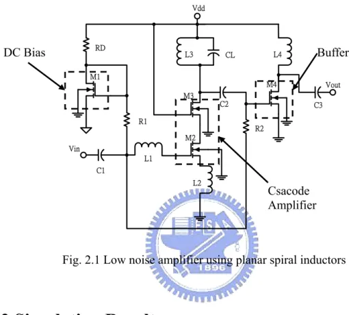
Following the circuit design given in [19], and with details presented in another reference [20], the complete circuit is shown in Fig. 2.1. It was found that a two-stage amplifier is required to achieve the desired gain and to provide a good isolation between input and output. The first stage is a cascode amplifier consisting of M2 and M3. L1 and L2 are for input matching. L3 and CL form a tank circuit to tune the LNA to 2.4GHz. M4 is the output stage with a matching network of L4 and C3. M1, R1, and RD form a bias circuit. M1
is a current mirror with RD, while R1 prevents the bias circuit from shunting the RF input signal. C1, C2, and C3 are used as a DC blocking capacitor. Vin and Vout are input/output source voltage ports respectively.
C1 C2 C3 CL L1 L2 L3 L4 RD R1 R2 Vin Vout Vdd M1 M2 M3 M4 Buffer DC Bias Csacode Amplifier
Fig. 2.1 Low noise amplifier using planar spiral inductors
2.1.2 Simulation Results
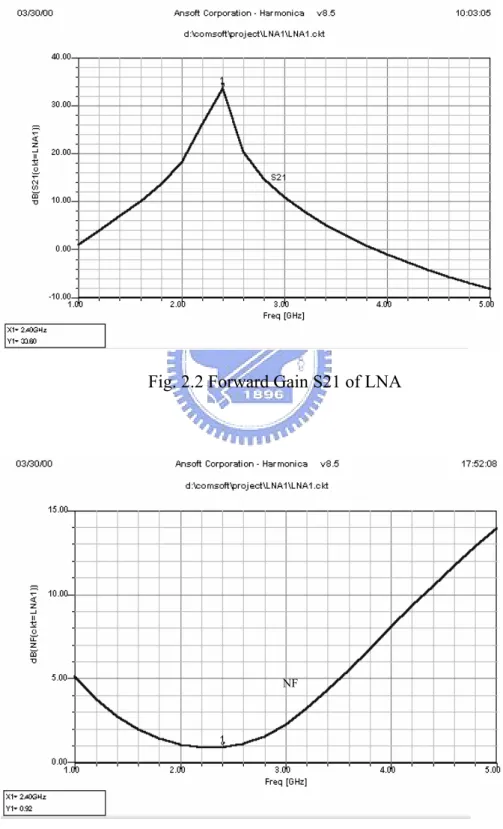
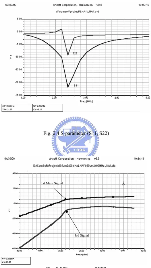
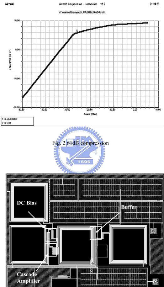
The proposed circuit was simulated using Serenade 8.5 simulator. All transistor models are Bsim3v3 for TSMC 0.35 um process. Fig. 2.2 shows the forward gain of LNA. The amplifier provides a forward gain of 33dB at 2.4GHz. Noise Figure (NF) is obtained and shown in Fig. 2.3. Simulation results show that this LNA achieves a noise figure of 1dB at 2.4GHz. Both S11 and S22 parameters of LNA are illustrated in Fig 2.4. The simulated S11 and S22 are –23dB, -9dB respectively. The linearity of this LNA, which is normally evaluated by the input referred third-order intercept point (IIP3), is plotted in Fig. 2.5. The simulated IIP3 is around 0dBm. Fig. 2.6 shows the response of input power versus output power, which indicates the 1dB compression point. The simulated 1dB compression point
is –26dBm. The complete layout of the LNA circuit, shown in Fig. 2.7, was realized by TSMC 0.35um CMOS technology with a die size of 850um×600um. The LNA drains 10.8mA from a 3.3V supply and the power dissipates 35.6mW at 2.4GHz frequency.
Fig. 2.2 Forward Gain S21 of LNA
NF
Fig. 2.4 S-parameter (S11, S22)
3rd Signal 1st Main Signal
Fig. 2.61dB compression
DC Bias
Buffer
Cascode Amplifier
2.1.3 Discussion
In this section, we have demonstrated a low noise amplifier in a standard TSMC CMOS 0.35um process. The amplifier was applied with planar spiral inductors. Based on the simulation results, we believe that CMOS is a suitable technology for wireless transceiver design and will provide the integration of a complete communication system on a single chip. Although the amplifier reaches acceptable performance, many of the drawbacks exist in the amplifier. Especially, the area of the planar spiral inductors is much larger than the others components, such as active devices (MOSFET). In additional, to obtain an accurate passive spiral inductor is very difficult. During the process of IC manufacturing, any change within the processing stage will affect the characters of the inductor. Moreover, the characters changed would also generate certain character change within the whole circuits. Meanwhile, the Q-value of a planar spiral inductor is very low, in which its range is from 12 to 15. So, for obtaining a higher power gain, we must raise the circuit bias current. However once we raise the bias current, the power consumption will also increase at the same time. For improving the disadvantages mentioned above, we applied the advantages of using active inductors. This solution of using an active inductor not only lowers the die size and provides higher Q-value but also decreases the power consumption of the circuits. Moreover, we can use the external bias voltage to revise the unpredictable effects caused by the processing change during the IC manufacturing stage, and this solution also helps to minimize the change of the circuit characters. Therefore, an active inductor is the best alternative to improve drawbacks using the planar spiral inductor.
2.2 Characteristics of Active Inductors
Based on the principle, the characteristics of an active inductor circuit can be obtained and operated in the radio frequency range. The active inductor circuit produces characteristics of inductance impedance. The inductance impedance includes both the real term and the imaginary term. These terms can be also called the loss and the inductance, respectively. The real term and the imaginary term of the inductance impedance are fundamental factors to describe the characteristics of the active inductor. Therefore, the important parameters of an active inductor can be defined by the real term and the imaginary term of the inductance impedance, such as the quality-factor (Q), the inductance (L), and the resonant frequency (ω0). In addition, these parameters can be used to analyze the performance of an active inductor circuit as well.
Traditionally, active inductors are typically created by using high gain operational amplifiers with negative feedback, and are thus unsuitable for frequencies close to the fT of the transistors. An alternative strategy, which has been proposed, was using GaAs, MESFET and bipolar technologies [27, 40] to exploit capacitance with the transistors to implement the require inductance impedance. Since these techniques make use of the parasitic within the devices, the circuits can operate close to the technology limits. These parasitic methods seem promising for the implementation of high frequency active inductors in CMOS technology.
The basic principle of forming the active inductor circuit is based on a well-known gyrator theory [30]. The gyrator topology is a two-port network that can be realized by connecting in parallel and back-to-back two voltage-controlled current source of opposite polarities. Fig. 2.8 shows an arrangement of an active inductor implementation based on a capacitive load gyrator topology.
Fig. 2.8 Gyrator topology
From the input terminal in Fig. 2.8, this architecture of the gyrator simulates inductance impedance (Zin), expressed as Eq. (2.1).
1 2 in in in m m V sC Z I G G = ≈ (2.1)
where Gm1 and Gm2 are the transconductor of the amplifier.
In order to obtain a CMOS active inductor, the active inductor can be operated in the radio frequency band. The simplest active inductor based on a gyrator topology can be realized by using a single MOS transistor as the transconductance (Gm) element, as shown in Fig. 2.9. The active inductor exploits the intrinsic capacitances within the transistors to achieve the require poles and zeros. As a result, the active inductor is capable of operating up to the cut off frequency (ft) of the transistors.
M1 M2 I1 I2 Zin Vd d
In the Fig. 2.9, if each transistor is modeled by cgs, cgd, gm, and gds, the model is shown in Fig. 2.10, and then the input impedance (Zin) of the circuit of the Fig. 2.9 can be derived in Eq. (2.2).
Fig. 2.10 A small-signal model of the MOS transistor
2 1 2 1 2 1 1 2 1 2 ( ) ( )( ( gs gd gd ds in gd ds m gs gd m s C C C g Z sC g g s C C ) g ) + + + ≈ + + + + (2.2) where s=jω , based on a first order small signal analysis and the assumption of the Cgdi << Cgsi, the Eq. (2) can be simplified in Eq. (2.3).
2 1 2 2 1 2 2 Re( ) Im( ) ( )( ) gs ds in in in gd ds m gs m sC g Z Z j Z sC g g sC g + ≈ = + + + + (2.3)
or can be expressed as input conductance (Yin).
2 1 1 2 2 1 2 2 1 2 2 2 1 2 1 [ ] ( )( Re( ) Im( ) gs ds in gd ds m gs m m m ds m gs gs ds in in sC g Y sC g g sC g g g g g sC sC g Y j Y ) − + ≈ + + + = + + + + = + (2.4)
From Eq. (2.3), the input impedance, Zin, is equivalent to the input conductance Yin. The input impedance Zin can be formed with the real term and the imaginary term, and Zin is the
equivalent RLC network for the active inductor, shown in Fig.2.11. The values of all components in the Fig. 2.11 can be derived by Eq. (2.3) or Eq. (2.4), and be expressed as Eq. (2.5) to Eq. (2.8).
Fig. 2.11 Equivalent RLC model of active inductor
2 2 p ds m m G =g +g ≈g 2 (2.5) 1 p g C =Cs (2.6) 2 1 2 gs m m C L g g = (2.7) 1 1 2 ds s m m g R g g = (2.8)
In additional, the self-resonant frequency for the active inductor is expressed in Eq. (2.9) and the Q-value at the self-resonant frequency ω0 can be written as Eq. (2.10).
2 1 2 0 1 2 m m gs gs g g C C ω = (2.9) 0 2 1 2 2 2 1 1 1 gs m m L ds ds gs C g g C Q g g C ω = = gs (2.10)
Therefore, based on the gyrator configuration, the circuit can obtain the equivalent input inductance impedance (Zin), which produces the required parameters and includes both the real term and the imagine term to simulate an inductor. Then the equivalent input
In CMOS RF front-end circuits, the inductors are the fundamental component for filtering, tuning, phase shifting and matching. To achieve the required specifications in RF application circuits, a high performance inductor must be obtained. The characteristics of the inductor should basically possess a high quality factor (high Q-value), a wide inductance range, and a high operating frequency. Because a higher Q-value will obtain a higher selection, a higher gain, and a lower phase noise in RF circuit applications. A wider inductance range and a higher operating frequency will achieve more an effective inductor and a higher frequency circuit. Therefore, in CMOS RF active inductor designs, a higher Q value, a wider inductance range, and a higher operating frequency are expected.
An inductor is a component of storage energy. To store the energy for a long period of time in the inductor, the loss of the inductor should be as small as possible. Similarly, an active inductor simulates the characteristic of inductance based on active devices. The characteristic of a high-Q value CMOS active inductor implies the loss of the inductor circuit must be as small as possible.
The equivalent impedance of an inductor can be expressed as a combination of the resistance and the inductance, shown in Fig.2.12. According to the definition of the Q-value of the inductor, the Q-value can be defined as Eq. (2.11).
Zin
Rloss
jXL Rloss+jXL
Fig. 2.12 The equivalent circuit of inductor
Im( ) Re( ) in L Z X Q Z R = = (2.11)
From Eq. (2.3) and Fig. 2.12, the input equivalent impedance of the active inductor combines both the real term and the imaginary term. It is called loss and inductance, respectively. The equivalent input impedance of the active inductor can also be expressed as the combination of the resistance and the inductance, shown in Fig. 2.12. And the Q value of the active inductor can be defined in Eq. (2.11) as well.
Therefore, the Q-value of the active inductor will be affected by the loss (the real term) and the inductance (the imaginary term). In order to obtain a higher Q-value, a higher inductance and a lower loss are required.
2.3 CMOS Active Inductors and Applications
Recently, CMOS active inductors and their applications have been published in the literature [33-37]. The topologies of the active inductors were implemented by using the gyrator configuration. The circuit type of the published active inductors was constructed with the common source (CS) and the common drain (CD), shown in Fig.2.9, and was connected with the common gate (CG) and the common source, which shows in Fig. 2. 13. These circuits formed the basic configurations of the active inductors.
M1 M2 I1 Zin VG S S Vd d
For the active inductor research, improving the Q value and the low operating voltage have been the trends [36-39]. The techniques of improving the characteristics of active inductors using the gain boosting, the current-reused, the double feedback, and the negative conductance compensated techniques, shown in Fig. 2.14 to Fig.2.16 have been described, respectively. Fig. 2.17 is the architecture of the negative impedance technique used to improve the Q value of the active inductor.
M
1M
2M
3I
1I
2Z
inV
GV
ddFig. 2.14 Gain boosting compensated active inductor
M
1M
2I
1Z
inV
G S SV
ddIr
Although the proposed techniques can improve the Q value of the active inductor, the inductor circuits posses some drawbacks such as the complexity and power consumption. In addition, in order to operate on a low voltage, the active inductor circuit used the PMOS transistor, shown in Fig. 2.18, was proposed.
M
1M
2M
3I
1I
GZ
inV
11V
ddI
SI
2M
11M
PV
GFig. 2.16 Double feedback compensated active inductor
-R
R+jX
L Active Inductor Negative ImpedanceZ
inM
1M
2I
1I
2Z
inV
ddV
GFig. 2.18 Low voltage active inductor
For the applications of active inductors, the bandpass filters [36, 39], the low noise amplifier [32], the bandpass amplifier [24, 31], and the voltage-controlled oscillators [35, 37] based on previous research have been published [33-37]. Although, these applications have good performances, the performances can further be improved by improving the characteristics of the active inductor.
2.4 Summary
In this chapter, we will summarize the disadvantages of using planar spiral inductors to design the amplifier. The disadvantages are listed as the following: causing a larger die size and a lower Q-value, requiring more power consumption, and producing the revising difficulties. The above disadvantages can be overcome by using active inductor. The principle operation methodologies of an active inductor are based on the application of the gyrator.The gyrator configuration of using active devices can be used to simulate the active inductor to obtain the inductance impedance. The Q value and the inductance of the active inductor will
be affected by the transconductance and the capacitance of the MOSFETs. The external bias voltage will tune the transconductance of the MOSFETs. Therefore, the external bias voltage can vary the characteristics of the active inductor.
Though there are several successful solutions for enhancing the characters of the active inductors and have proposed in the literatures, there are still some other simpler ideas that have stronger capabilities to improve the characters of the active inductor. So, we will propose those simpler approaches in chapter 4.
Chapter 3
Designs of the RF Amplifiers Using CMOS
Active Inductors
Motivated by the growing market of RF communications system, much effort has been devoted to the implementation of RF circuits in a CMOS technology. A low noise amplifier is the most demanding block in a RF system. The specifications of a low noise amplifier must be satisfied the following requirements which include larger power gain, lower noise figure, better impedance matching, good linearity, lower power consumption, and lower manufacturing cost. These demanded requirements have been traditionally led to the implementation of the discrete components or the use of exotic processes. Inductors are fundamental for the design of low noise amplifiers. Most of the published low noise amplifiers are implemented by using chip passive spiral or bond wire inductors. The quality factor of an integrated planar spiral inductor is normally low. For producing a higher quality factor, an integrated inductor requires additional processing steps. By applying techniques proposed in [6], it is possible to compensate the quality factor of these inductors for reducing extra manufacturing cost. Moreover, the un-tunable inductor value is dependent on the size of the inductor [24]. Thus the additional tuning circuitry is required to modify the required characteristics in our applications and it is also the main problem when we consider
minimizing the size of an inductor. For reducing the size of a traditional integrated passive inductor, an active inductor will be introduced to achieve the goals of downsizing the chips.
In this chapter, the design of the low noise radio frequency amplifiers, which are called the active inductors, are presented. Several low noise amplifier simulations using different active inductors and a negative conductance generator were performed and the simulation results showed that the characteristics of the low noise amplifiers are improving and various frequencies are operated via different combining designs of active inductors and a negative conductance generator. Especially, the occupied chip area of the low noise amplifier is significantly reduced and the characteristics of the low noise amplifiers can directly tune by using external voltage.
The organization of this chapter is as the following. In section 3.1, a 2GHz CMOS LNA with the regulated cascade active inductor and the source follower negative conductance generator is illustrated. In section 3.2, a 2.4GHz CMOS low noise amplifier with the high-Q active inductor load is proposed. Finally, a brief summary is made in section 3.3.
3.1 A 2GHz CMOS LNA with Active Inductor and Source
Follower Negative Conductance Generator
In this RF low noise amplifier, the regulated cascode active inductor and the source follower negative conductance generator (NIC) are used to design the amplifier. The regulated cascode active inductor is described in section 3.1.1. The source follower negative conductance generator circuit based on a common drain with common gate is given in section 3.1.2. The design methodology of the low noise amplifier is given in section 3.1.3. The simulation results of the low noise amplifier are shown in section 3.1.4. Finally, the discussion is given in section 3.1.5.
3.1.1 Regulated Cascode Active Inductor
An often-used way to produce an active inductor is to combine a gyrator and capacitor. The circuits proposed in Fig. 3.1 exploit the parasitic within the devices and the active inductors proposed can operate in the GHz range. In order to increase the quality factor Q, the Q-enhancement technology are proposed to increase the quality factor of the active inductor. The technique is used to exploit the regulated cascode technology, which reduces the inductor loss and increases the cascode gain. Based on the first small signal analysis, the equivalent RLC network of the inductor is shown in Fig. 3.2.
M
8M
9M
3I
1I
3Z
inV
ddI
2M
11Fig. 3.1 Regulated cascode active inductor
G
pC
pL
R
sZ
in3.1.2 The Source Follower Negative Conductance
Generator
A negative conductance generator is proposed to enhance the quality factors of the active inductor. A common drain stage combines with a common gate stage to generate the source follower negative conductance generator as depicted in Fig. 3.3. The main idea of this design is to generate an out-of-phase output current respected to the input current and feed it back to the applied input voltage at the same node, which is called the positive feedback configuration. Transistor M6 is a transistor providing transconductance gain gm6. Transistor M5 forms a simple current mirror, providing the out-of-phase function and the voltage gain. Transistor M4 provides a required DC current through the negative conductance generator. Based on the combining configuration of M4 to M6, the equivalent negative conductance will be generated.
Assuming gmi >> gdsi for all transistors and ignoring all non-dominant
higher-order-terms, the conductance of the negative conductance generator can be expressed as: 5 6 5 6 m m n m m g g G g g − = − +
The idea of reducing the loss is to add a source follower negative conductance generator to the active inductor so that the loss of the active inductor can be compensated. The negative conductance generator produces the negative conductance –Gn to connect in
Fig. 3.3 The negative conductance generator
3.1.3 Low Noise Amplifier Design Methodology
A common gate CMOS low noise amplifier with a regulated cascode active inductor load and a source follower negative conductance generator will be presented in this section. In order to improve the power gain of the low noise amplifier, a large impedance of the load is required. Thus, the current running on the impedance should be minimized for obtaining a large impedance load, and the size of transistor can also be minimized. Moreover, the dimension of transistors should be increased to generate a large bias current for obtaining good linearity. Therefore, trade-offs between the power gain and linearity should be taken into account. An alternate configuration, combining with the regulated cascode active inductor and the source follower negative conductance generator are used to increase the impedance load. In other words, increasing the Q-value of the active inductor can obtain the large impedance load. In order to increase the Q-value, the loss of the active inductor should be reduced. The source follower negative conductance generator generates the negative conductance (–Gn) connected in parallel with the active inductor. The loss of the active
inductor can be reduced.
Therefore, a low noise amplifier, which has the features of higher gain, smaller chip size, and lower power consumption, is proposed. The configuration of the proposed low noise
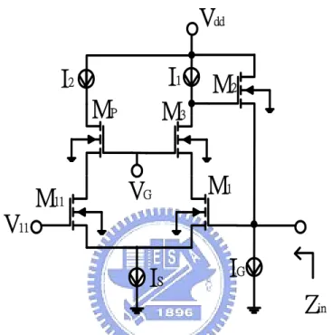
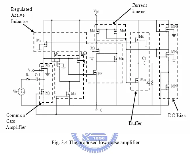
amplifier consisting with four signal-processing stages is illustrated in Fig. 3.4.
Fig. 3.4 The proposed low noise amplifier
In Fig. 3.4, the first stage, transistors M1 and M2 comprise the input amplifier stage.
This common-gate configuration provides a simple 50-Ohm input impedance matching and higher linearity in contrast to a common-source configuration without source degeneration. This common-gate configuration also helps to increase the effective reverse isolation in heterodyne architectures due to the signal leakage of the local oscillator from the mixer to the antenna. The second stage, a regulated cascode active inductor is constructed by transistorsM3, and M7~M11. The regulated cascode active inductor acts as the load of the low
noise amplifier. The equivalent circuit model of the active inductor is shown in Fig. 3.2. The source follower negative conductance can help reduce the inductor loss of the regulated
M11 are formed the active inductor constant current source. The third stage, a source follower
negative conductance generator is constructed by transistors M4~M6. The main idea of this
stage is to generate an out-of-phase current respected to the input current and feed it back to the input voltage at the same node called the negative conductance generator, which compensates the loss of the active inductor. Therefore, it is possible to improve the quality factor of the active inductor. The final stage, the output voltage buffer is built up by transistors M12 and M13. A voltage buffer follows the designed amplifier in order to drive a
50-Ohm resistive load and it also requires a large drain current to drive a low resistance load. The transistors of MN1 to MN3 produce the bias voltage to provide the voltage the transistors
M1, M4, M9, M11, and M12. The capacitors of the C1 and the C2 are the dc coupling to block
the dc voltage so that the external bias voltage will not affect the bias of the amplifier.
3.1.4 Simulation Results
The low noise amplifier was simulated by parameters from a standard CMOS 0.35-um digital process technology using HSPICE simulator. The normal supply voltage is 3.3V. Figs. 3.5, 3.6 and 3.7 show the simulation results of S21, S11, S12, S22, and noise figure where the amplifier is tuned around 2GHz. It can be seen that S21 is 17.6dB and S11, S22, and S12 are –11.2dB, -11.9dB, –39.4dB, and 5.05dB around 2GHz, respectively.
In RF amplifier, the conditions (necessary and sufficient) for unconditional stability are expressed in following: 2 2 2 11 22 12 21 1 1 2 S S D k S S − − + = > , where D S S= 11 22−S S12 21 2 12 21 1 11 S S < − S
2 12 21 1 22
S S < − S
From Fig. 3.5 and 3.6, at f = 2GHz, we find that K = 1.31 and D = 0.174∠160 ゚. Since K > 1 and |D| <1, the amplifier is unconditional stable. Furthermore, in the frequency range between 1.6GHz and 2.4GHz shows the K > 1 and |D| <1, the amplifier will be unconditional stable.
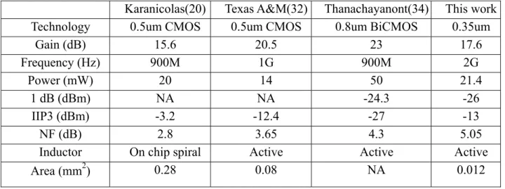
The 1dB compression and the IIP3 are -26dBm and -13dBm, respectively, and are shown in Fig. 3.8 and Fig. 3.9. From Fig. 3.8 and 3.8, the linearity of the proposed amplifier can achieve reasonable requirements. The layout of the low noise amplifier is shown in Fig. 3.10. From Fig. 3.10, the area of the proposed circuit is 108um×104um, which is smaller than that of the amplifiers use the passive spiral inductor of the previous work. Furthermore, the power consumption of the low noise amplifier is 21.4mW, which is smaller than that others design. A comparison between our design using the regulated cascode active inductor with the negative conductance generator of source follower configuration and other designs reported in the literature is presented in TABLE 3.1.
Fig. 3.6 S22 and S12 of the low noise amplifier 0 2 4 6 8 10 12
1.6E+09 1.7E+09 1.8E+09 1.9E+09 2.0E+09 2.1E+09 2.2E+09 2.3E+09 2.4E+09
Frequency
dB
Noise Figure
-30 -20 -10 0 10 -40 -35 -30 -25 -20 -15 -10 Pin, dBm Pout , dB m 1 dB Compression
Fig. 3.8 1dB compression of the low noise amplifier
IIP3 -40 -30 -20 -10 0 10 -35 -30 -25 -20 -15 -10 Pin, dBm Pout, dBm 1st Main Signal 3rd Signal
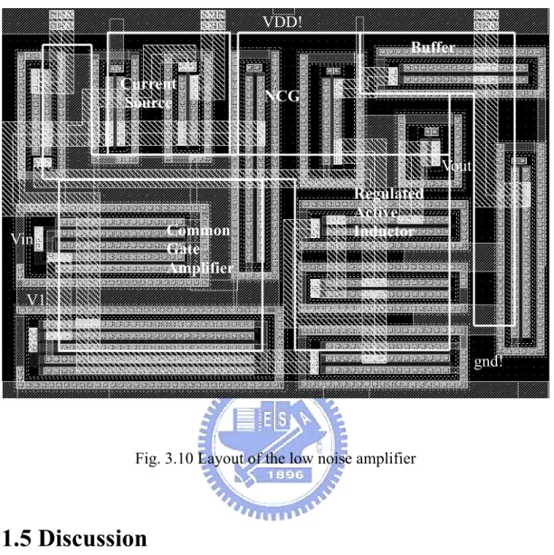
VDD! gnd! Vin V1 Vout Current Source NCG Buffer Regulated Active Inductor Common Gate Amplifier
Fig. 3.10 Layout of the low noise amplifier
3.1.5 Discussion
This work presents the design of a CMOS low noise amplifier using the regulated cascade active inductor and the source follower negative conductance generator as the frequency selective element and the Q-enhancement. The proposed circuit is verified by HSPICE simulation and the results show that the center frequency and the power gain of the low noise amplifier are electronically tunable. The performance of the low noise amplifier is better than that of the integrated passive inductor. The achievement of this work is to reduce the size of the chip to 108um×104um.
TABLE 3.1 COMPARISONS OF 2 GHZ LOW NOISE AMPLIFIERS
Karanicolas(20) Texas A&M(32) Thanachayanont(34) This work Technology 0.5um CMOS 0.5um CMOS 0.8um BiCMOS 0.35um
Gain (dB) 15.6 20.5 23 17.6 Frequency (Hz) 900M 1G 900M 2G Power (mW) 20 14 50 21.4 1 dB (dBm) NA NA -24.3 -26 IIP3 (dBm) -3.2 -12.4 -27 -13 NF (dB) 2.8 3.65 4.3 5.05
Inductor On chip spiral Active Active Active
Area (mm2) 0.28 0.08 NA 0.012
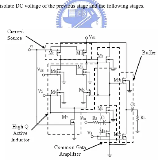
3.2 A 2.4GHz CMOS Low Noise Amplifier with High-Q
Active Inductor Load
In this RF low noise amplifier, a double feedback cascode active inductor is used to design the amplifier. The double feedback cascode active inductor acts as the load of the low noise amplifier to obtain reasonable requirements. In this work, the cascode active inductor is introduced in section 3.2.1. In section 3.2.2, the double feedback technique is presented to improve the Q-value of the cascode active inductor. The design methodology of the low noise amplifier is given section 3.2.3. Simulation results of the low noise amplifier are shown in section 3.2.4. Finally, the discussion is given in section 3.2.5.
3.2.1 Cascode Active Inductor
An often-used way to produce active inductors is by combining a gyrator with two transconductors connected in back-to-back configuration and a capacitor. The cascode active inductor shown in Fig. 3.11 exploits the parasitic within the devices.
Fig. 3.11 The cascode active inductor
As shown in Fig. 3.11, transistor M3 is used to convert the input voltage Vs, into a
current for charging the integrating capacitor Cgs3, whereas M2 is used to convert the voltage
across Cgs2 into an input current Is. Base on a small signal analysis, the equivalent circuit for
this inductor is also shown in Fig. 3.2. Where, 2 1 m g R= 3 gs C c= 5 3 2 5 3 m m m ds ds L g g g g g r = 3 2 2 m m gs
g
g
c
L
=
In this configuration, the gain boosting is the utilization of negative feedback around the cascode common-source amplifier comprising of M3 and I1 to reduce the series resistive loss.
Hence, gain-boosting techniques have been applied to M3 in order for increasing its voltage
gain, gds3gds5/gm3gm5 for cascode configuration. However, referring to Fig. 3.2, the gain boosting technical operation does not affect the parallel resistive loss and its value left to be finite (about 1/gm2) so that an important characteristic on Q enhancement is limited. Intuitively, this effect arises from the existence of undesirable coupling path formed by cgs2 and cgs3, which spoil the current, Is, from M2 and M3 at high frequency. In order to diminish
the parallel resistive loss, positive feedback has been placed around the first transconductor (M3) in the active inductor for compensating the excessive currents in cgs2 and cgs3.
3.2.2 Q-Enhancement Active Inductor
The Q-value of the cascode active inductor in Fig. 3.11 can be improved by removing the parallel resistive loss and series resistive loss. Thus the cascode common source configuration in Fig. 3.11 can be replaced with a pair cascode common source around the cascade common source as illustrated in Fig. 3.12.