Modified resistive switching behavior of Zr O 2 memory films based on the interface
layer formed by using Ti top electrode
Chih-Yang Lin, Chung-Yi Wu, Chen-Yu Wu, Tseung-Yuen Tseng, and Chenming Hu
Citation: Journal of Applied Physics 102, 094101 (2007); doi: 10.1063/1.2802990
View online: http://dx.doi.org/10.1063/1.2802990
View Table of Contents: http://scitation.aip.org/content/aip/journal/jap/102/9?ver=pdfcov Published by the AIP Publishing
Articles you may be interested in
Multilevel resistive switching in Ti / Cu x O / Pt memory devices J. Appl. Phys. 108, 114110 (2010); 10.1063/1.3518514
Effects of Ti top electrode thickness on the resistive switching behaviors of rf-sputtered ZrO 2 memory films Appl. Phys. Lett. 95, 112904 (2009); 10.1063/1.3231872
Improvement of resistive switching characteristics in TiO 2 thin films with embedded Pt nanocrystals Appl. Phys. Lett. 95, 042104 (2009); 10.1063/1.3193656
Formation of multiple conductive filaments in the Cu / ZrO 2 : Cu / Pt device Appl. Phys. Lett. 95, 023501 (2009); 10.1063/1.3176977
Pulse-induced low-power resistive switching in Hf O 2 metal-insulator-metal diodes for nonvolatile memory applications
J. Appl. Phys. 105, 114103 (2009); 10.1063/1.3139282
Modified resistive switching behavior of ZrO
2memory films based on the
interface layer formed by using Ti top electrode
Chih-Yang Lin, Chung-Yi Wu, Chen-Yu Wu, and Tseung-Yuen Tsenga兲
Department of Electronics Engineering and Institute of Electronics, National Chiao Tung University, Hsinchu 300, Taiwan
Chenming Hu
Department of Electrical Engineering and Computer Sciences, University of California at Berkeley, California 94720, USA
共Received 13 July 2007; accepted 7 September 2007; published online 1 November 2007兲 The influence of Ti top electrode material on the resistive switching properties of ZrO2-based
memory film using Pt as bottom electrode was investigated in the present study. When Ti is used as top electrode, the resistive switching behavior becomes dependent on bias polarity and no current compliance is needed during switching into high conducting state. This phenomenon is attributed to the fact that a series resistance between Ti and ZrO2film, composed of a TiOxlayer, a ZrOylayer,
and even the contact resistance, imposed a current compliance on the memory device. Besides, our experimental results imply that switching the device into high conducting state is a field driven process while switching back into low conducting state is a current driven process.
© 2007 American Institute of Physics.关DOI:10.1063/1.2802990兴
I. INTRODUCTION
Recently, a resistive switching phenomenon observed in various oxide films in metal-insulator-metal 共MIM兲 struc-tures has been developed for potential nonvolatile memory application. Based on previous studies, the origin of the re-sistive switching is mainly associated with the intrinsic bulk property, but the interface between electrodes and oxide films also has a considerable influence on the resistive switching phenomenon. Therefore, various surface treat-ments and various materials with different top and bottom electrodes combinations were studied to further look into the mechanism of the resistive switching phenomenon.1–9Seo et
al. investigated the resistive switching in the top electrode/
NiO / Pt structures, demonstrating that, if the top electrode formed an Ohmic contact with NiO film, the effective elec-tric field inside the film became high enough to cause the resistive switching. On the contrary, if well-defined Schottky contact was formed, there was a voltage drop across the in-terface so that the electric field across the NiO was too small to induce resistive switching. Choi et al. reported that the resistive switching has only been observed in Al/ TiO2/ Pt
devices when applying positive bias on Al top electrode, pro-posing that the electrode-relative bi—or unipolar resistive switching seems to be related to the oxygen permeation through the top electrode. Sawa et al. studied the current-voltage 共I-V兲 characteristics of different top electrodes stacked on the Pr0.7Ca0.3MnO3共PCMO兲/SrRuO3 bottom
electrode, concluding that a Schottky-like barrier was the main factor determining the resistive switching phenomenon. Peng et al. tried to explain the Schottky-like barrier causing resistive switching through the correlated work function
fac-tor influencing resistive switching of symmetric metal/ PCMO/metal structures with electronegativity of different metals electrodes.
In this study, the resistive switching behavior of ZrO2
films in MIM structure with Ti top electrode was investi-gated. TiOxand ZrOy共y⬍2兲 interface layers were formed at
the interface of Ti top electrode/ZrO2film, leading to the fact
that the resultant I-V curve was significantly different from that without TiOxand ZrOyinterface layers. A uni-to-bipolar
resistive switching translation is demonstrated to give an in-sight into resistive switching mechanism.
II. EXPERIMENT
40⬃70-nm-thick ZrO2 films were deposited on
Pt/ Ti/ SiO2/ Si substrates at 250 ° C by a radio-frequency共rf兲
magnetron sputtering. All ZrO2 films were prepared at
10 mTorr, which was maintained by a gas mixture of oxygen and argon at a mixing ratio of 6:12. To achieve the MIM structure, a 150-nm-thick Ti top electrode was deposited by rf magnetron sputtering or electron beam evaporation at am-bient temperature with a diameter of 250m patterned by the shadow mask process. The base pressure for sputtering Ti top electrode was 2⫻10−6Torr using a cryopump and the
working pressure of Ar gas 共99.995%兲 was kept at 7.6 ⫻10−3 Torr during deposition process. The base pressure for
electron beam evaporation was 4⫻10−6Torr using a cry-opump. Agilent 4155C semiconductor parameter analyzer was used to measure the I-V characteristics of the ZrO2film memory device at room temperature.
III. RESULTS AND DISCUSSION
Figure1shows a schematic diagram of the device struc-ture and measurement system. The I-V characteristics were measured in a two-probe configuration, and the bias voltage a兲Electronic mail: [email protected]
0021-8979/2007/102共9兲/094101/5/$23.00 102, 094101-1 © 2007 American Institute of Physics
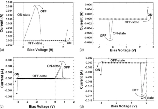
was applied on Ti top electrode with the Pt electrode grounded. Figure2 depicts that the unipolar and bipolar re-sistive switching phenomena can be observed by using a tungsten probe directly contacting with ZrO2/ Pt structures
without Ti top electrode 共W probe/ZrO2/ Pt兲, which
demon-strates that both positive and negative voltages can perform the reproducible resistive switching. After high voltage form-ing process, the W probe/ZrO2/ Pt devices are switched into
high conducting state共on state兲. on state can be switched into low conducting state共off state兲 by applying positive voltage bias, and back into on state again by positive or negative voltage bias, as shown in Figs. 2共a兲 and 2共b兲. Figures2共c兲 and2共d兲show that on state can be also switched into off state by negative voltage bias, and back into on state by positive or negative bias. As a result, the resistive switching is inde-pendent of bias polarity, and the influence from the interface of the ZrO2/bottom electrode and/or the interface of tungsten
probe/ZrO2 is negligible. That is because most of interface
effects relate to bias polarity based on previous report,4but the result shown here is not related to the bias polarity. The bulk of ZrO2 film dominates the resistive switching.
Because Ti is an oxygen-gettering metal, using Ti as the
top electrode is expected to modify the oxygen content, oxy-gen vacancies, oxyoxy-gen ions, and oxyoxy-gen-related defect dis-tribution in the ZrO2 films, and further causes the formation
of a TiOxand a ZrOylayer. According to the result of
sec-ondary ion mass spectrometry共SIMS兲 analysis, as shown in Fig.3, the signal of TiO is detected and there is a TiOxlayer
indeed formed at the interface of Ti/ ZrO2. However, the
ZrOylayer is difficult to be identified here, this is because the
ZrOylayer is so thin which is beyond the resolution of SIMS
analysis. Therefore, high-resolution transmission electron microscopy共HR-TEM兲 observation was carried out and the result is shown in Fig. 4. A thin interface layer about few nanometers is found and believed to be ZrOy, but the
differ-ence between Ti and TiOx, however, is indistinguishable in
the HR-TEM image. Based on the results of SIMS profile and HR-TEM image, the interface layer formed between Ti and ZrO2 would comprise TiOx and ZrOy, and this device
structure can be defined as Ti/ IL/ ZrO2/ Pt, where IL
pre-FIG. 1. A schematic diagram of the device structure and the measurement system.
FIG. 2. Resistive switching behavior performed with positive and negative bias voltages showing unipolar and bi-polar resistive switching by using tungsten probe directly in contact with ZrO2/ Pt structure.
FIG. 3. SIMS depth profile of ZrO2/ Pt stack using Ti top electrode.
094101-2 Lin et al. J. Appl. Phys. 102, 094101共2007兲
sents interface layer consisting of TiOx and ZrOy. The
for-mation of the TiOxlayer is caused by Ti metal reacting with
O2presented in the chamber during deposition and the inter-diffusion between Ti and ZrO2 film, and the ZrOy layer is
formed due to the interdiffusion between Ti and ZrO2 film.
As a result, the TiOxlayer is much thicker compared with the
thin ZrOy layer, as shown in Fig. 3. Furthermore, it is
ex-pected that there are tiny thickness and stoichiometry varia-tions of the TiOxlayer between two different techniques for
Ti top electrode deposition in the experimental part due to different fabrication conditions, such as base pressure, work-ing pressure, and Ar usage, but the I-V characteristics of these two kinds of memory devices are almost the same. Hence, one of the possible reasons attributed to this phenom-enon is that the different Ti deposition techniques might in-duce very similar ZrOy layers, and their TiOx layers only
play a minor role. Another possible reason might be that the variation of process-dependent interface layers in this study does not significantly change the I-V characteristics. Future work is going to focus on controlling the interface layers by depositing various thicknesses of Ti metal on ZrO2films, and
to provide more detailed study about the effect of various kinds of interface layers on the electrical characteristics of ZrO2 films.
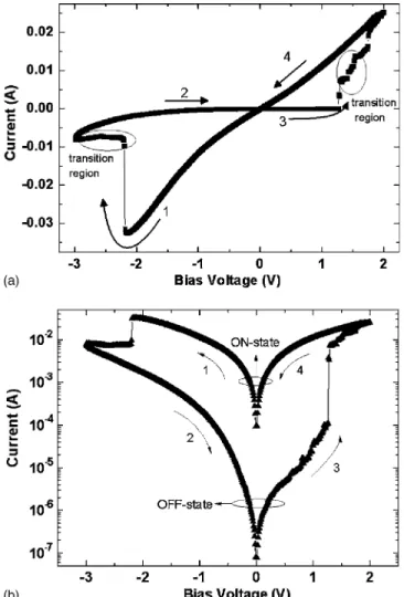
The typical I-V characteristics of Ti/ IL/ ZrO2/ Pt device in linear scale, translating into bias polarity dependent, are shown in the Fig. 5共a兲. The same I-V characteristics are shown also as a semilogarithmic plot in the Fig.5共b兲. Only
by applying positive voltage bias can switch the
Ti/ IL/ ZrO2/ Pt device into on state, and it can be switched
back into off state only by negative voltage bias, demonstrat-ing that bipolar resistive switchdemonstrat-ing occurs when usdemonstrat-ing Ti top electrode for the MIM structure. Before any resistive switch-ing is performed, a formswitch-ing process, which can be achieved by either positive or negative voltage bias with a current compliance of 5 mA at an absolute value of 5 – 8 V, is nec-essary for both Ti/ IL/ ZrO2/ Pt and W probe/ZrO2/ Pt
de-vices. Because both Ti/ IL/ ZrO2/ Pt and W probe/ZrO2/ Pt
devices possess the same forming process, Ti top electrode is
believed to only modify the top part of ZrO2 film instead of
the whole film. The forming process, independent of bias polarity and of top electrode, is analogous to the time depen-dent dielectric breakdown 共TDDB兲 in Pt/NiOy/ Pt devices,
and it was proposed that the conducting filaments were formed during dielectric breakdown.10Therefore, conducting filaments are believed to be present in Ti/ IL/ ZrO2/ Pt and W
probe/ZrO2/ Pt devices as a result of forming process.
More-over, due to the resistive switching phenomenon and similar forming process observed in both Ti/ IL/ ZrO2/ Pt and W
probe/ZrO2/ Pt devices, we would conclude that the ZrO2
film, instead of interface layers, dominates the resistive switching behavior, while the interface layers serve as a se-ries resistance and an oxygen sink. We are going to elucidate how interface layers influence the resistive switching behav-ior in the following section.
After a forming process, the Ti/ IL/ ZrO2/ Pt was
switched from original state into on state. Subsequently, the negative bias voltage applied on the top electrode changes the device from on state to off state, and the turn-off process is marked in region 1, as shown in Fig.5共a兲. While positive voltage is applied on the Ti top electrode again to switch the device into on state, the current compliance is not needed, which is obviously different form the I-V curves of other
FIG. 4. Cross-sectional HR-TEM image of a thin ZrOy interface layer
formed between Ti共TiOx兲 and ZrO2.
FIG. 5. 共a兲 Typical I-V curve of the Ti/IL/ZrO2/ Pt device in linear scale,
applying positive bias on Ti top electrode to switch the device on and nega-tive bias to switch it off.共b兲 I-V curve in semilog scale.
metal oxides resistive switching devices previously reported. The interface layers in series with the ZrO2 film act as a current compliance resistance during turn-on process. Before any sudden change in ZrO2resistance, most of voltage drop
is across the ZrO2film for its off state with larger resistance
than that of the interface layers. After a sudden resistance change in the ZrO2film at 1.3 V, the resistance of ZrO2film
is close to that of the interface layers at this time, and the voltage drop across the ZrO2 decreases to near half of the
initial value. The more the resistance of ZrO2film decreases,
the lower the voltage drop across the ZrO2film is, leading to
a transition region presented in the region 3. Finally, most voltage drop is across the interface layers. Consequently, the interface layers impose a current compliance during turn-on process and this way is similar to current limited by transis-tor gate voltage proposed by Chen et al.11
During turn-off process, the transition region also ap-pears in region 1 due to the same reason why the TiOxlayer
is still in series with the ZrO2film and the resistance of ZrO2
is comparable to that of the interface layers at this moment. Moreover, the conducting filaments continue rupturing dur-ing sweepdur-ing of the bias voltage from −3 to 0 V. The char-acteristics of the Ti/ IL/ ZrO2/ Pt device, where interface lay-ers play roles of a series resistance, are obviously demonstrated in this study. In addition to the interface layers, it is worthy noting that the contact resistance might also play an important role for the series resistance.
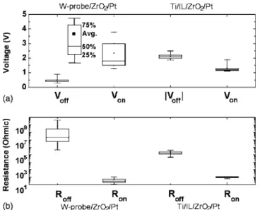
In general, conducting filaments are thought to be easily formed where local electrical field is especially high, and it can propagate through the insulator until conducting connec-tions are formed between the electrodes. Consequently, the biased electrons find one or few conducting paths consisting of possible point defects, such as oxygen vacancies and other ionic and electronic defects.7 Simultaneously, the electrons hopped passing through the insulator in these paths and caus-ing the current to dramatically increase, and this is the on process. In Fig. 6共a兲, the turn-on voltage of the Ti/ IL/ ZrO2/ Pt device, in general, is smaller than that of the
W probe/ZrO2/ Pt devices. A smaller voltage is enough to
provide large effective electric field inside the ZrO2 films leading to the formation of conducting filaments. This is due to the ZrO2films modified by the Ti top electrode to reduce the effective resistive switching region. Therefore, the turn-on process can be thought to be a field driven process. Moreover, the effective resistive switching region is reduced so that the Ti/ IL/ ZrO2/ Pt device possesses lower variations
in Voff, Von, Roff, and Ron 共as shown in the Fig.6兲 and lower
resistance ratio between on state and off state.
Another interesting phenomenon is that the Ron of Ti/ IL/ ZrO2/ Pt device is larger than that of W probe/ ZrO2/ Pt device, which might be due to the interface layers formed in series with the conducting filaments in the ZrO2
matrix. For higher Ronof Ti/ IL/ ZrO2/ Pt device, the turn-off
voltage of the Ti/ IL/ ZrO2/ Pt device is expected to be higher
than that of the W probe/ZrO2/ Pt device under the same off
current, which conforms to the statistical results, as shown in Fig. 6. Besides, some reports proposed that for the higher current compliance imposed on the device to switch into on state, higher off current was needed to switch it into off state.12,13 Based on above results, the off process can be in-terpreted to be a current driven process.
On the other hand, the large variation in Roff may be
caused by the random rupture of the conducting filaments,14 implying that the region for filament rupture might be large. Kim et al. have reported that thin IrO2 layers, located
be-tween Pt and NiO films in the device of Pt/ NiO / Pt, would stabilize local oxygen migrations for filament formation and rupture, resulting in the stable resistive switching parameters.15In our Ti/ IL/ ZrO2/ Pt device, the interface lay-ers would have the same function as the above mentioned IrO2layer, and fix filament formation and rupture at a certain
region. Moreover, the region for filament rupture in the W probe/ZrO2/ Pt device is expected to be wider than that in the
Ti/ IL/ ZrO2/ Pt device to some degree, leading to its Roff
higher than that of the Ti/ IL/ ZrO2/ Pt device. Consequently,
the value and the variation of Roff in the W probe/ZrO2/ Pt
device are larger than those of the Ti/ IL/ ZrO2/ Pt device due to the different top electrode used.
The off process is believed to be related to the rupture of the conducting filaments, which is considered to occur at high resistance flaws inside the filaments by local Joule heating.16Kinoshita et al. suggested that the turn-off process may be realized by oxidization of the whole or a part of the conducting filaments on the anodic side.8Based on their sug-gestions, the off process is thought to be a current driven process due to the local Joule heating enhancing the oxidiza-tion of parts of conducting filaments, resulting in the rupture of conducting filaments. The oxidization assisted by local Joule heating effect takes place on the anodic side of the conducting filaments, which is close to the electrode with positive bias, causing the off process. It could be used to explain why the Ti/ IL/ ZrO2/ Pt device cannot be switched
off by applying positive bias, for the reasons that the oxidiza-tion takes place in the interface layers instead in the parts of the conducting filaments near Ti top electrode. Therefore, when applying negative bias on the Ti top electrode to switch off the device, the oxidization assisted by the local Joule
FIG. 6. Variations of the resistive switching parameters in the W-probe/ ZrO2/ Pt and Ti/ IL/ ZrO2/ Pt devices, respectively. Ronand Roffare the
re-sistances measured at 0.3 V for each device.
094101-4 Lin et al. J. Appl. Phys. 102, 094101共2007兲
heating is expected to take place in the parts of the conduct-ing filaments near Pt electrode which is the anodic side rela-tive to the Ti top electrode.
The detailed mechanism of resistive switching behavior remains unclear. The existence of oxygen ions and vacancies would play an important role in resistive switching,7,17 lead-ing to reduction and oxidization in some parts of conductlead-ing filaments. When Ti is applied with positive bias, oxygen ions migrate to the interface layers, accompanied by oxygen va-cancies diffused toward Pt electrode, causing the reduction of conducting filaments and switching into on state. When Ti is applied with negative bias, electrons injected from Ti top electrode cause oxygen ions to migrate from the interface layers to oxidize the conducting filaments, switching into the off state. It has been reported in our recent paper that the Ti/ IL/ ZrO2/ Pt device indicated a little degradation of
elec-trical performance after successive switching cycles,8 which might be possibly related to the evolution of the interface layers considering this work. Further study is necessary to investigate the evolution of the interface layers after degra-dation of the memory device and to closely look into the interrelations between the interface layers formed and origi-nal mechanism of the resistive switching behaviors.
IV. CONCLUSION
In summary, the effects of the Ti top electrode and the interface layers on the resistive switching characteristics of Ti/ IL/ ZrO2/ Pt device were investigated in this study. It was
found that such an effect leads to a translation from unipolar to bipolar resistive switching. Moreover, a series resistance formed due to the existence of the TiOxlayer, and even the
contact resistance between Ti and ZrO2 film imposed a cur-rent compliance on the memory device during turn-on pro-cess, which is different from those reported in the literatures. The turn-on process can be regarded as a field driven process and the turn-off process can be interpreted to be a current driven process owing to the local Joule heating enhancing the oxidization of anodic parts of conducting filaments.
ACKNOWLEDGMENTS
This work was partly supported by the Taiwan Semicon-ductor Manufacturing Company, Ltd., and by the National Science Council, Taiwan, under Project No. 95-2221-E-009-278.
1S. Seo, M. J. Lee, D. C. Kim, S. E. Ahn, B.-H. Park, Y. S. Kim, I. K. Yoo,
I. S. Byun, I. R. Hwang, S. H. Kim, J.-S. Kim, J. S. Choi, J. H. Lee, S. H. Jeon, S. H. Hong, and B. H. Park, Appl. Phys. Lett. 87, 263507共2005兲.
2B. J. Choi, D. S. Jeong, S. K. Kim, C. Rohde, S. Choi, J. H. Oh, J. Kim,
C. S. Hwang, K. Szot, R. Waser, B. Reichenberg, and S. Tiedke, J. Appl. Phys. 98, 033715共2005兲.
3W. C. Peng, J. G. Lin, and J. H. Wu, J. Appl. Phys. 100, 093704共2006兲. 4A. Sawa, T. Fujii, M. Kawasaki, and Y. Tokura, Appl. Phys. Lett. 85, 4073
共2004兲.
5H. Sim, H. Choi, D. Lee, M. Chang, D. Choi, Y. Son, E.-H. Lee, W. Kim,
Y. Park, I. K. Yoo, and H. Hwang, Tech. Dig. - Int. Electron Devices Meet.
2005, 777.
6C. Y. Liu, P. H. Wu, A. Wang, W. Y. Jang, J. C. Young, K. Y. Chiu, and T.
Y. Tseng, IEEE Electron Device Lett. 26, 351共2005兲.
7C. C. Lin, B. C. Tu, C. C. Lin, C. H. Lin, and T. Y. Tseng, IEEE Electron
Device Lett. 27, 725共2006兲.
8C. Y. Lin, C. Y. Wu, C. Y. Wu, T.-C. Lee, F.-L. Yang, C. Hu, and T.-Y.
Tseng, IEEE Electron Device Lett. 28, 366共2007兲.
9C. Y. Lin, C. Y. Wu, C. Y. Wu, C. Hu, and T. Y. Tseng, J. Electrochem.
Soc. 154, G189共2007兲.
10K. Kinoshita, T. Tamura, M. Aoki, Y. Sugiyama, and H. Tanaka, Appl.
Phys. Lett. 89, 103509共2006兲.
11A. Chen, S. Haddad, Y.-C. Wu, T.-N. Fang, Z. Lan, S. Avanzino, S.
Pan-grle, M. Buynoski, M. Rathor, W. Cai, N. Tripsas, C. Bill, M. VanBuskirk, and M. Taguchi, Tech. Dig. - Int. Electron Devices Meet. 2005, 765.
12S. Seo, M. J. Lee, D. H. Seo, E. J. Jeoung, D.-S. Suh, Y. S. Joung, I. K.
Yoo, I. R. Hwang, S. H. Kim, I. S. Byun, J.-S. Kim, J. S. Choi, and B. H. Park, Appl. Phys. Lett. 85, 5655共2004兲.
13C. Rohde, B. J. Choi, D. S. Jeong, S. Choi, J.-S. Zhao, and C. S. Hwang,
Appl. Phys. Lett. 86, 262907共2005兲.
14B. J. Choi, S. Choi, K. M. Kim, Y. C. Shin, C. S. Hwang, S.-Y. Hwang,
S.-s. Cho, S. Park, and S.-K. Hong, Appl. Phys. Lett. 89, 012906共2006兲.
15D. C. Kim, M. J. Lee, S. E. Ahn, S. Seo, J. C. Park, I. K. Yoo, I. G. Baek,
H. J. Kim, E. K. Yim, J. E. Lee, S. O. Park, H. S. Kim, U.-I. Chung, J. T. Moon, and B. I. Ryu, Appl. Phys. Lett. 88, 232106共2006兲.
16D. C. Kim, S. Seo, S. E. Ahn, D.-S. Suh, M. J. Lee, B.-H. Park, I. K. Yoo,
I. G. Baek, H.-J. Kim, E. K. Yim, J. E. Lee, S. O. Park, H. S. Kim, U.-I. Chung, J. T. Moon, and B. I. Ryu, Appl. Phys. Lett. 88, 202102共2006兲.
17M. Fujimoto, H. Koyama, M. Konagai, Y. Hosoi, K. Ishihara, S. Ohnishi,
and N. Awaya, Appl. Phys. Lett. 89, 223509共2006兲.