I
使用 3D 有限時域差分法分析相位移光罩接觸孔
之近場
Simulation on using 3D Finite difference time domain
to analysis near field in Phase Shift Mask Contact
Hole
研 究 生:王 昱 鈞 Yu-Jun Wang
指導教授:羅 正 忠 博士 Dr. Jen-Chung Lou
A Thesis
Submitted to
Department of Electronics Engineering & Institute of Electronics
College of Electrical and Computer Engineering
National Chiao Tung Unicersity
in Partial Fulfillment of the Requirements
For the Degree of Master
In
Electronic Engineering
June 2007
Hsinchu, Taiwan, Republic of China
II
使用 3D 有限時域差分法分析相位移光罩接觸孔
之近場
研究生:王昱鈞 指導教授:羅正忠 博士
國 立 交 通 大 學
電子工程學系 電子研究所
碩 士 論 文
摘要
在使用氟化氬並配合高數值孔徑的微影技術去曝 65 奈米的圖形以進入了接 近 0.3 的 k1 參數值,以及光罩圖形使用的波長以四倍的量值.此外,相位移光罩為了 產生一百八十度的光程差所以去蝕刻一個特定深度的溝.由於波長和高的圖像縱 橫比,所以有厚度的光罩效應變成了模擬誤差的來源.尤其對相位移光罩產生很大 的影響.以及使用小波長三維精確的電場磁場做模擬. 在以前,因為柯希荷夫邊界條件下,我們得以使用一個較”薄光罩”去近似物體 的場,但在次波長微影技術的條件下,不得不需要考慮薄光罩的效應,所以一個新 的模擬方法被推出來使用,在基於類似薄光罩在晶圓上產生的場.他的名字叫做有 限時域差分法.他是為了在電腦模擬下,把馬克斯威爾方程式離散化.所以我們用 這個方法,去分析光罩的電場磁場繞射現象III
Simulation on using 3D Finite difference time domain
to analysis near field in Phase Shift Mask Contact
Hole
Student:Yu-Jun Wang Advisor:Dr. Jen-Chung Lou
Department of Electronics Engineering & Institute of Electronics
College of Electrical and Computer Engineering
National Chiao-Tung University
ABSTRACT
The using of ArF lithography with high numerical aperture (NA) to print 65nm wafer features translates into a k1 factor approaching values about 0.3 and mask
features of the order of the wavelength for 4X magnification. In addition, the Phase-shifting mask (Alt PSM) employ etching with a depths so that have a optical difference in order to make a 180° phase-shifting openings. As a consequence of wavelength sized and high aspect ratio mask features, thick mask effects are becoming a error source of simulation, which are particularly critical for Alt. PSM, and 3D rigorous electromagnetic field simulations in the sub-wavelength regime.
In the past, Kirchhoff's Boundary Conditions on the mask surface provides the so-called “Thin Mask” approximation of the object field. But for sub-wavelength lithography, however, it fails to account for thick mask effect A new simulation model is proposed, which is based on a comparison of the fields produced by the thick masks on the wafer. Which is Finite-Difference Time-Domain(FDTD). It can discrete
IV
the Maxwell’s equation to fit computer’s simulation. We can use FDTD techniques to view rigorous Simulation of electromagnetic scattering and diffraction.
V
誌
謝
在碩士研究的這二年歲月,首先要感謝的是我的指導教授 羅正忠教授並致 上我最誠摯的謝意。感謝老師在專業的通訊領域中,給予我不斷的指導與鼓勵, 並賦予了實驗室豐富的研究資源與環境,使得這篇碩士論文能夠順利完成。 其次,要感謝實驗室的學長—胡國信學長、張仲興學長在研究上的幫助與意 見,讓我獲益良多。感謝實驗室的同學—建彰,德安,人傑,等在課業及研究上的互 相砥礪與切磋,以及生活上的多彩多姿。感謝學弟們,讓實驗室在嚴肅的研究氣 氛中增添了許多歡樂,有了你們,更加豐富了我這二年的研究生生活。 最後,要感謝的就是我最親愛的家人,由於他們在我求學過程中,一路陪伴 著我,給予我最溫馨的關懷與鼓勵,讓我在人生的過程裡得到快樂,更讓我可以 專心於研究工作中而毫無後顧之憂。 鑒此,謹以此篇論文獻給所有關心我的每一個人。 王昱鈞 誌予 九十六年七月VI
Contents
---
Chapter1: Introduction………1
1.1 Introduction to optical lithography………1
1.2 Resolution Enhancement Techniques (RETs)………...3
1.2.1
Sub-Wavelength
Lithography………..5
1.2.2
Phase-Shifting
Masks………..6
1.2.3
Off-Axis
illumination………..7
1.2.3
Optical
Proximity Correction………...8
1.2.4
Focus-Latitude
Enhancement Exposure………..9
1.3 Rigorous Optical Imaging Modeling……….9
1.3.1 Vector Effects at High NA……….10
1.3.2 Mask Topography Effects………..11
Chapter2: Models of Fourier Optical in Lithography Imaging…………13
2.1 The Optical Lithography Exposure System ………....13
2.1.1
Scalar
Diffraction………...13
2.1.1
Vector
Diffraction……….16
2.2 The Process Window and Energy Latitude………..17
Chapter3: Finite Difference Time Domain………..20
3.1
FDTD
Method……….20
3.2 Perfectly matched layer ………..26
Chapter4: Simulation………30
4.1 Model of Simulation………30
4.2 Simulation Result………35
Chapter5: Conclusions……….49
VII
List of figure
---
FIG 1.1 Numerical Aperture(NA) FIG1.2 Depth of Focus(DOF) FIG1.3 The wavelength and DRAM
FIG1.4 A schematic view of a typical projection optical-exposure system and RET. FIG1.5 Working Principles of RETs
FIG1.5 The various types of PSMs.
FIG1.6 Effect of illumination angle on the amplitude profile at the pupil under (a) on-axis illumination and (b) off-axis illumination.
FIG1.7 (a) Scattering Bars, (b) Hammer Heads and (c) Serifs. FIG1.8 (a) TE-polarization, (b) TM-polarization
FIG1.9 Kirchhoff and rigorous condition
FIG 2.1Crossection view of the optical lithography exposure system FIG 2.2 The E-D window chart
FIG 2.3 The Bossong Plot
FIG 2.4 The chart to determine process window
FIG 3.1 backward, forward, central FD operator FIG 3.2 The FDTD cell in the simulation region
FIG 3.3 Upper-right part of a computational domain surrounded by the PML layer. FIG 4.1 Simulated Region(i=160,j=160,k=140 sizes)
FIG 4.2 The mask type M0, M1, M2, blue region: Qz; yellow region: Cr FIG 4.3 Wafer stack film
VIII
FIG 4.4 The near field amplitude and phase of the three type mask M0,M1,N2 FIG 4.5a,b M1 and M2 in Ex field amplitude
FIG 4.6 Poynting vector (j=160,k=140)
FIG 4.7 The cross section figure of Py in M1 structure. FIG 4.8 FDTD Simulation and Poynting vector
FIG 4.9 One wavelength intensity in 4 mode FIG 4.10 The Aerial Image in 3 mask type FIG 4.11 3 type contact hole on the same mask FIG 4.12 Not alignment and alignment M2 structure
1
Chapter1: Introduction
Optical Lithography represents the main manufacturing technology of integrated circuits (IC) today. Over the many years, lithography need to challenge to the smaller and smaller size, better known as Moore's Law [1], of doubling chip density roughly every eighteen months while maintaining a nearly constant chip price. Nowadays photolithography continues to enable this steady miniaturization of the wafer Critical Dimensions (CD, also call feature size) below the illumination wavelength through the utilization of ingenious techniques of resolution enhancement [2].
The fabrication of DRAM chips need the most advanced lithographic techniques. The half-pitch (mainly the distance between near memory 'cells' on the chip) is an important practical constraint in the fabrication of DRAMs. But more recently, the significant commercial pressure for increased performance and expansion of market size has resulted in the development of microprocessors, high-end logic large-scale integrated (LSI) circuits, and 'system-on-a-chip' LSI circuits that each use
smaller-scale patterning than the contemporary generation of DRAMs.
1.1 Introduction to optical lithography
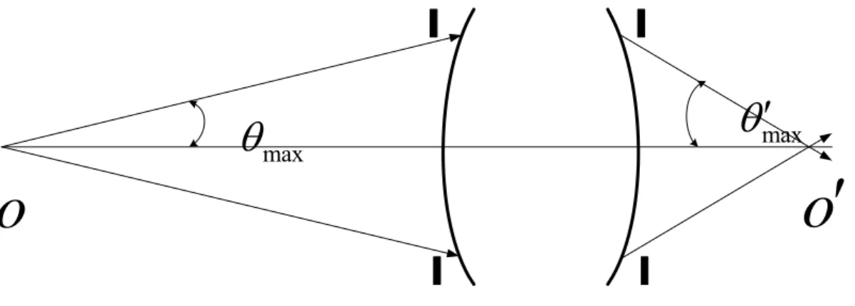
The numerical aperture (NA) of a lens is defined as: NA=nsinθmax ( the capability of lens system to capture the diffraction information of object.) ,where n is the refractive index of the imaging medium andθmaxis the maximum acceptance angle. The space at the entrance side of the lens is called object space, and the space at the exit side of the lens is called image space. As FIG 1.1 The numerical apertures on both spaces are related through the magnification of the system, M: o
i NA M NA = . Usually M=1 1,
2
The expression for the critical dimension is:
1
CD
k
NA
λ
=
Where k depend on the lithography process such as photoresist processing, 1 coherence of the illumination and wave manipulation and other process parameters, Physical limitations constrain k to be greater than 0.5 and 0.25 for coherent and 1 incoherent illumination, respectively.[3]
Images observed on planes out of focus become blurred and loose definition. The range of distances about the focal plane over which the image is adequately sharp according to certain specifications is defined as the Depth of Focus (DOF). This quantity can be seen to be governed by the following expression [4]:
As FIG 1.2,
o
o′
max
θ
θ
max′
FIG 1.1 Numerical Aperture(NA)
δ
S
w
OPD: optical path difference
Image position for reference (S) wavefront
Image position for defocused (W) wavefront
Exit pupil axis
FIG1.2 Depth of Focus(DOF)
3 We can know that OPD:
(
)
2 4 62
sin sin
OPD 1 cos sin
2 4 8 OPD sin 2 2 err δ θ θ δ θ θ λ δ θ π ⎛ ⎞ = − = ⎜ + + + ⎟ ⎝ ⎠ Φ ≈ + …
So Defocus can be expressed as err err 2 2 sin NA λ λ δ π θ π Φ ⎛Φ ⎞ = = ⎜ ⎟ ⎝ ⎠ 2 2 2
DOF , with process factor NA
k λ k
=
If the refractive index in the image space does not equal unity, then
2 2 2 2 DOF NA sin n k k n λ λ θ = =
Increasing the NA in an attempt to improve resolution results in a rapid degrada- -tion of the Rayleigh DOF. Furthermore, the photoresist has a finite thickness of the order of the DOF (0.3μm−0.8μm), thus the position of the plane of best focus must be controlled accurately to provide good image quality throughout the resist thickness. Depth of focus is another important factor in the resolution equation.
1.2 Resolution Enhancement Techniques (RETs)
The use of RET has become an absolute necessity for the manufacture of advanced integrated circuits. The demands of Resolution Enhancement Techniques (RETs) for Optical Lithography we can observe form FIG 1.3. To improve the resolution of an optical lithography system without introducing other impractical constraints (on, for example, wafer smoothness), several resolution-enhancement strategies have been proposed [5,6,7].And the FIG 1.4 shows a schematic view of a typical projection optical-exposure system include RET.
(1-2a)
(1-2c) (1-2b)
4
1970
1980
1990
2000
2010
100
1000
Minimum Feature S ize/E xposure wavelength (nm)Year
g-line i-line KrF ArF3000
300
30
F2 256K 1M 4M 16M 64M 256M 1G 4G Exposure wavelengthe reduction trend Miniaturization trend of DRAM pattern RETPractical resolution limit of projection lithography with High NA ~ λ/2
FIG1.3 The wavelength and DRAM
5
1.2.1 Sub-Wavelength Lithography
Refractive lenses with the required transparency and quality at 248nm wave- length can only be made of fused silica. Calcium fluoride (CaF2) can also be used in combination with fused silica at 193nm, what can improve the operating bandwidth, and it represents the principal candidate at 157nm. The lack of transparent optical components at shorter wavelengths limits the available wavelengths in Deep Ultraviolet lithography, which is now being performed within the sub-wavelength regime. This means that the minimum feature of the wafer circuit is smaller than the wavelength of the light source used to print it.
The utilization of 193nm wavelength lithography with a 0.85 NA to print 65nm wafer features translates into a k1 factor approaching values around 0.3 and mask
features of the order of the wavelength for 4X magnification. Several techniques of resolution enhancement (RETs) have been developed and are being increasingly employed, together with imaging systems of higher numerical aperture (NA), to overcome the limits of optical lithography.
+1st -1st 0th -1st +1st 0th +1st π π mask projection lens Aerial Image Conventional
Medium CoherencyPSM (alternated) Oblique illuminatio
Light Source
FIG1.5 Working Principles of RETs(b) (c) (a)
6
1.2.2 Phase-Shifting Masks
Phase-shifting masks (PSM) making the destructive interference of the fields with opposite phases. Masks are commonly classified into Binary and Phase-Shifting depending on whether the transmission coefficient through the mask takes only the values 0 and 1, or a certain amount of phase shift is introduced. Levenson's
Alternating PSM [5] introduce180 phase difference through two contiguous
apertures on the mask by etching the glass with a depth difference equivalent to180
(
1)
,
180 .
360
d
n
φ φ
λ
− =
=
The principle of operation of both binary and Alternating Phase-Shifting masks is compared in FIG1.5(a),(b). it enhance fine features of the image and
reducing the DC background. There are several different types of phase shift masks. The various types of masks are presented in FIG 1.6. Among them, alternating phase shift masks in (b), the phase edge masks, and attenuated phase shift masks in (d) [8,9,10]are the most interesting in practical application.
FIG1.5 The various types of PSMs.
7
1.2.3 Off-Axis illumination
When on-axis illumination is used on periodic gratings,FIG1.5(a), both
diffraction orders with indexes +1 and -1 need to be collected by the lens to produce interference. In addition the 0th-order is also collected, which carries DC background. By illuminating at an off-axis angle,FIG1.5(c), the image can be formed by
interference of the 0thdiffraction order and either one of the± orders. 1
FIG1.6 Effect of illumination angle on the amplitude profile at the pupil under (a) on-axis illumination and (b) off-axis illumination. The interference pattern of f 0 and f 1 under on-axis illumination is rapidly upward to compensate intensity as defocus, while that under off-axis illumination behaves as a slowly varying function of defocus.
8
In FIG 1.6(a). we examine the two-beam interference pattern of the negative innermost Fourier component ( f 0) and positive outermost one ( f 1) along the optical axis direction to elucidate the influence of oblique illumination because most of the spectrum energy is concentrated around these two spatial frequencies. When the mask is illuminated by an off-axis point source, the diffraction pattern is shifted off optical axis so that these two spatial frequencies are distributed on alternated sides of the axis FIG 1.6(b). The two-beam interference pattern has a cosinusoidal distribution with a period described in the form [11]:
2 2 2 2
period=
1
NA
1 (1
)
NA
λ
σ
σ
−
−
− −
where σ denotes the ratio of the sine of illumination angle to the projection lens NA. If σ =0,then it become to on-axis illumination
2
period=
1
1 NA
λ
−
−
1.2.3 Optical Proximity Correction
For the condition that not all corrections applied to the mask shapes are
necessarily to account for effects of the proximity of other features, it is customary to refer to all adjustments of the mask features compensating for low k1 effects as
Optical Proximity Corrections (OPC).
OPC applied to sparse features to simulate a dense environment. These are called Scattering Bars or Assist Features and they are sub-resolution geometries that do not print on the wafer because all the high spatial frequencies are filtered out by the lens. As FIG 1.7 mention:
(1-4a)
9
1.2.4 Focus-Latitude Enhancement Exposure
Hitachi invented a new method for increasing the depth of focus in 1987 lithography engineers[8], which they termed Focus Latitude Enhancement Exposure (FLEX). In FLEX several focal planes are created at different positions along the light axis, and exposures are made using each focal plane. It has two exposures are superposed in FLEX. One has a focal plane in the upper level and the other in the lower level. Each exposure is made in the same place on the substrate for the same mask pattern. And later, he use this theory to change the mask or pupil function mention as “super FELX”[9].
1.3 Rigorous Optical Imaging Modeling
In the past, we let the masks are designed using a number of approximations: 1. The mask is infinitely thin,
2. The mask material is perfectly absorbing,
(a) (b) (c) FIG1.7 (a) Scattering Bars, (b) Hammer Heads and (c) Serifs.
10
3. Simple scalar Fraunhofer diffraction can account for all the mask’s effects.
But as we consider the thick mask effect. There are a number of physical effects taking place on these diffraction masks that are not captured by this simple model. The list of problem areas includes:
1. Real materials - leakage and surface plasmons, 2. Thick masks - sidewall reflections,
3. Sidewall geometry - reflections and glowing corners,
4. Polarization - mask openings have different effective areas depending on polarization.
1.3.1 Vector Effects at High NA
The preceding derivation of the scalar theory of Fourier optics neglects the vector nature of light. For high numerical aperture systems, e.g., for NA = 0.7 and above, the approximations and simplifications made throughout fail and the oblique propagation of the waves becomes important. The most obvious vector diffraction effects arise from polarization in the illumination producing orientation-dependent asymmetries in the printed patterns. For example, in the case of phase-shifting masks or off-axis illumination the aerial image strongly depends on whether polarization parallel or perpendicular to the lines and spaces is used. In this section we follow the imaging part of Yeung's key work [12] and summarize the fundamental results there from using our notation.
11
From the FIG 1.8, we can get the idea why TE-polarization is better then TM-polarization. For reason that the vector summation difference in the focus point
1.3.2 Mask Topography Effects
Sub-wavelength lithography places a serious limitation on the conventional ”thin mask” approximation of the field immediately behind the patterned mask. This approximation fails to account for the increasingly important topographical effects of the mask or ”thick mask” effects. This approximation of the photomask near-fields results from the direct application of Kirchhoff Boundary Conditions, which multiply the incident field by a binary transmission function of the patterned mask. Polarization dependent edge diffraction effects, as well as phase and amplitude transmission errors that arise from the vector nature of light, and the finite thickness of the substrate and chrome layers, produce significant errors in the scalar simulations of the lithographic image[13].
FIG1.8 (a) TE-polarization, (b) TM-polarization
12
As FIG 1.9 mention, in the past year, we compute an aerial image for a contact hole by transform a rectangular function. But now, if we consider the thick mask effect, we need to transform function the amplitude structure in the FIG 1.9(b)
FIG1.9 Kirchhoff and rigorous condition
13
Chapter2: Models of Fourier Optical in
Lithography Imaging
2.1 The Optical Lithography Exposure System
2.1.1 Scalar Diffraction
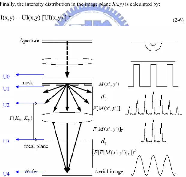
The FIG 2.1 is the view of the optical lithography imaging. In this figure, we can know the different field with different stage, and what is this stage influence to the field. We divide the field into U0,U1,U2,U3,U4. As [14] mention.
First of all, we have some definition:
0 0 0 2 : _ , : _ _ _ , : _ _ _ ' : _ _ _ _ _ _ ' : _ _ _ _ _ _ _ _ x y k propagation number
k k propagation number in x y direction wavelength in free space
f
f the ratio of focal lenght to wavelength D
D the ratio of diameter of projection lens to wavelength r π λ λ λ λ = − = = 1 2 ( ) 2 ( 1 : _ _ _ _ : _ { ( , )}: _ { ( , )}: _ _ { ( , )} ( , ) ( , ) { ( , )} ( , ) x y x lens i x y x y i x x y x y
the radius of projection lens NA numerical aperture
F f x y Fourier transform
F f x y inverse Fourier transform
F f x y f x y e dxdy f F f f e π σ σ π σ σ σ σ σ σ σ − + − + − = = =
∫∫
∫∫
) ', ', , ; yy x y y x x y d d k k x y x y k k σ σ σ σ σ λ λ = = = =x’,y’ is the real space’s position.
First, we consider a singular wave U0 behind the mask, and the mask function is M(x,y), after passing mask , field becomes to U1:
14 2 ( ) 0
0
1
( , ) 0
x y i x yU
E e
U
M x y U
π σ +σ=
=
And U1 can divide into many plane waves, after propagating a distance d ,we 0 can add these all plane wave to get U2. In the mathematical meaning is that let U1 do Fourier Transform, and multiply the phase term affect by propagating a distanced . 0 At last doing inverse Fourier Transform:
2 2 0 2 2 0 2 ( 1 ) 2 1
2
1
{ 1}
x y x y x y i x y d i dU
U e
dxdy
F U e
π σ σ σ σ π σ σ ∞ ∞ + + − − −∞ −∞ −=
=
∫ ∫
For the reason that lens area is not infinite, so from step U2 to step U3, it will filter some frequency components. So we multiply a phase difference term after projection lens, and we multiply a pupil function
∏
2 2 2 2 2 2
3
2
i f x y(
)
lensx
y
U
U e
r
π − + ++
=
∏
And the function:
∏
( ) 1, 0
x
=
if
< < =
x
1; 0,
otherwise
At the last step form U3 to U4, it is the same as from U1 to U2: 2 2
1
2 1
4
{ 3}
i x y dU
=
F U
e
π −σ −σIf we make these equation more simply, we can let it just a form:
-1
x
UI(x,y) = F {H(
σ σ
, y)F{M(x,y)}}Where H(σ σx, y)describes the propagation of the individual Fourier components (2-1)
(2-2)
(2-3)
(2-4)
15
inside the system. It can be calculated from the pupil function of the projection system., whereσ σx, y is refer to the spatial frequencies domain coordinates of the object . The aperture stop of a projection system has a finite size and thus accepts only Fourier components of the object spectrum inside a certain range. The maximum acceptable angle α specifies the NA of the system according to NA = (σ
x 2 +σ y 2 )1/2 = sin α. .Whether a specific Fourier component is transmitted or blocked by the
projection system depends on the shape of the projector entrance pupil . This effect is taken into account through the coherent transfer function H(σ
x,σy).
Finally, the intensity distribution in the image plane I(x,y) is calculated by:
I(x,y) = UI(x,y) [UI(x,y) ] *
U0
U1
U2
U3
U4
FIG 2.1Crossection view of the optical lithography exposure system
0
d
1
d
16
2.1.1 Vector Diffraction
For the condition that if Numerical Aperture is larger, then we need to consider TE, TM wave decouple effect, so we can calculate the distribution of the light intensity more correctly. If the wave propagating direction is (σxx,σyy,σzz). And the incident area’s normal vector is equal to wave propagation direction. So the propagating direction equal cross product of the (0,0,1) and plane wave’s propagating direction in the resist plane.
2 2 (0,0,1) ( , , ) ( , ) | (0,0,1) ( , , )| x y z y x x y z x y n σ σ σ σ σ σ σ σ σ σ × − = = × +
For the reason that TE direction the same as n-direction.
2 2 ( y, x) TE x y e
σ σ
σ
σ
− = +And the magnitude of the E is: TE
2 2 2 2 y x TE TE x y x y x y
E
E e
σ
E
σ
E
σ
σ
σ
σ
−
= •
=
+
+
+
And the magnitude of the TM field is the cross product of the TE field and the plane wave propagating direction in the lens:
2 2 2 2 (0,0,1) x y TM TE x y x y x y E E e
σ
Eσ
Eσ
σ
σ
σ
= • × = + + +And the direction is the cross product of TE direction and plane wave direction in the resist plane:
(2-7)
(2-8)
(2-9)
17 2 2 2 2 ( , , ) ( ) | ( , , )| TE x y z x z y z x y TM TE x y z x y e x y z e e
σ σ σ
σ σ
σ σ
σ
σ
σ σ σ
σ
σ
× + + + = = × + So we can get : 2 2 2 2 2 2 [ ] [ ( ) ] y x x y TE TE TE y x x y x x y y TM TM TM x z y z x y x y E E E E e x y E E E E e x y zσ
σ
σ
σ
σ
σ
σ
σ
σ σ
σ σ
σ
σ
σ
σ
− = = − + + = = + + + +2.2 The Process Window and Energy Latitude
In the process from exposure to development,for the reason to get the required CD we must confirm our dose and focus at constant. But it is usually affected by the correctly and stability of the stepper, the light dose and the focus may deviate from our setting value, and it will lead to the distortion of the image quality. If it is in the range of our tolerance, then the incorrectly of the stepper is considered to be
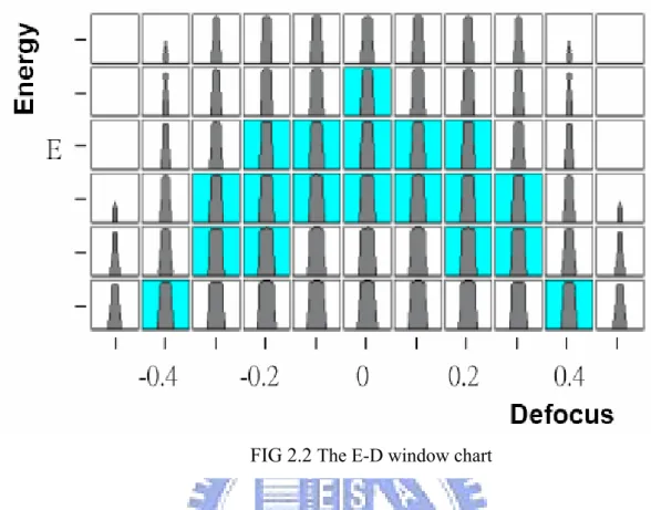
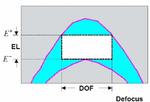
acceptable. We first must choose our CD target to determine the DOF of the process. If the shift of CD which in the range of n% is acceptable, then the spec of maximum CD is (1+n%)CD and the spec of minimum CD is (1-n%)CD . Then we can change the exposure dose or defocus , and we can get a matrix chart like FIG 2.2, we call this ”E-D window”(Energy-Defocus window)(or Bossong Plot, like a smile as the FIG 2.3, simultaneously we can pick the region where the CD is in the spec. By properly fitting we can get the FIG 2.4, and then we can get the max defocus range at the constant Energy Latitude (EL), and the range is the DOF of the process. The rectangle inner region that is surrounded by the EL and DOF is also called the “process window”.
(2-11)
(2-12)
18
FIG 2.2 The E-D window chart
19
20
Chapter3: Finite Difference Time Domain
In order to analyze the electromagnetic field (EMF) vector E and vector H in near field. We introduce the Finite Difference Time Domain (FDTD) algorithm from Kane YEE [15], which discrete the Maxwell’s equations, and using second order central-difference method. So we can know the vector E and vector H in any position in the simulation space. If we want to know more acknowledge. Ref[19].As the simulation space is not infinite, so we also using Perfectly Matched Layer (PML)[16],[17],[18]method in absorbing boundary condition.
3.1 FDTD Method
First, we need to know the Finite Difference (FD) Method 1-D FD Operators:
As the Taylor series:
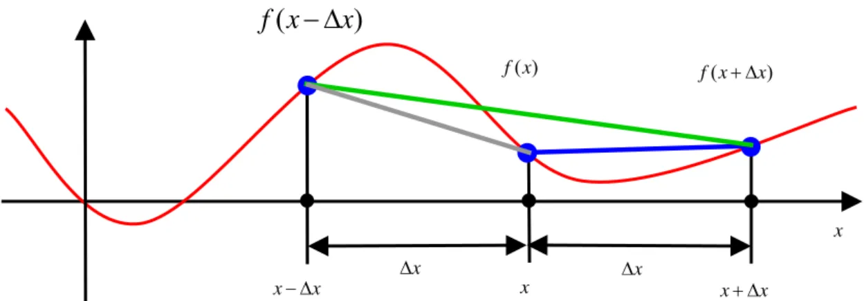
There are three method to describe the d ( )
dx f x
Which O( ) term is high order term, as the
Δ
x
smaller ,we can neglect this term. As FIG3.1 2 2 3 3 4 4 5 2 3 4 d ( ) ( ) d ( ) ( ) d ( ) ( ) d ( ) ( ) ( ) + + ( ) d 2! d 3! d 4! d f x x f x x f x x f x f x x f x x x x x x x Δ Δ Δ ⎡ ⎤ + Δ = + Δ + +d ⎣ Δ ⎦ 2 d ( ) ( ) ( ) ( ) ( ) ( ) d d ( ) ( ) ( ) ( ) ( ) ( ) d d ( ) ( ) ( ) ( ) ( ) ( ) ] d 2 2 f x f x x f x f x x f x x x x x f x x f x f x x f x f x x x x x f x x f x x f x x f x x f x x x x x − − Δ − − Δ = Δ ≈ Δ Δ + Δ − + Δ − = + Δ ≈ Δ Δ + Δ − − Δ + Δ − − Δ = + Δ ≈ Δ Δ + O O O [ (3-1) (3-4) Backward FD operator: Central FD operator: Forward FD operator:21
We can use this method to discrete the Maxwell’s equations.
0 H E t E H J t E H μ ε ε ρ μ ∂ ∇ × = − ∂ ∂ ∇ × = + ∂ ∇ ⋅ = ∇ ⋅ =
and for a linear, isotropic nondispersive material :
E
D
H
B
ε
μ
=
=
where: 0 0 r rε ε ε
μ μ μ
=
=
x Δ Δx x x− Δx x+ Δx x ( ) f x(
)
f x
− Δ
x
( ) f x+ ΔxFIG 3.1 backward, forward, central FD operator
(3-5a) (3-5b) (3-5c) (3-6a) (3-6b) (3-5d)
22 And the index is:
: electric field
: electric displacement field (also called the electric flux density) : magnetic field (also called the auxiliary field)
: magnetic flux density(also called the magnetic inducti E D H B -9 0
on or the magnetic field)
: free current density (not including polarization or magnetization currents bound in a material) : electric permittivity 1 : free-space permittivity( 10 ) 36 : relative perm r J ε ε π ε × -7 0 ittivity : magnetic permeability : free-space permeability(4 10 ) : relative permeability : curl operator : divergence operator r μ μ π μ × ∇× ∇⋅ In the 1D FDTD, we have
Constitutive Equations for Vacuum:
0 0
( , )
( , )
( , )
( , )
B R t
H R t
D R t
E R t
μ
ε
=
=
The electric and magnetic field in 1D :
( , )
( , )
( , )
( , )
x x y yE R t
E
z t e
H R t
H
z t e
=
=
WhereR
=
xe
x+
ye
y+
ze
z We choose in 1D: m e ( , ) ( , ) ( , ) ( , ) ( , ) ( , ) B R t E R t J R t t D R t H R t J R t t ∂ = − ∇ × − ∂ ∂ = ∇× − ∂ (3-7) (3-8) (3-9)23 m 0 0 e 0 0 1 1 ( , ) ( , ) ( , ) 1 1 ( , ) ( , ) ( , ) y x y x y x H z t E z t J z t t z E z t H z t J z t t z μ μ ε ε ∂ = − ∂ − ∂ ∂ ∂ = − ∂ − ∂ ∂
And we discrete it by the form:
2 2 ( 2 2 ( ) ( ) ] 2 2 ( ) ( ) ] t t f t f t d f t t dt t z z f z f z d f z z dz z Δ Δ ⎛ + ⎞− ⎛ − ⎞ ⎜ ⎟ ⎜ ⎟ ⎝ ⎠ ⎝ ⎠ = + Δ Δ Δ Δ ⎛ + ⎞− ⎛ − ⎞ ⎜ ⎟ ⎜ ⎟ ⎝ ⎠ ⎝ ⎠ = + Δ Δ O[ O[ we can get the 1D FDTD equation:
1 1 2 2 1 1 1 2 2 1 2 1 1 1 1 ( , , ) ( , , ) 2 2 2 2 1 1 ( , , 1) ( , , ) 2 2 1 1 ( , 1, ) ( , , ) 2 2 1 1 ( , , ) ( , , ) 2 2 1 1 1 1 ( , , ) ( , , ) 2 2 2 2 1 1 ( , , ) 2 2 n n x x n n y y n n z z n n x x n n z z n y B i j k B i j k t E i j k E i j k z E i j k E i j k y D i j k D i j k t H i j k H i j k y H i j k H + − − − − − + + − + + Δ + + − + = Δ + + − + − Δ + − + Δ + + − + − = Δ + + − − 1 2 1 2 1 1 ( , , ) 2 2 1 ( , , ) 2 n y n x i j k z J i j k − − + − Δ + +
If we use this method to find 3D-FDTD, then the (3-1a) and (3-1b) are equivalent the following equation:
(3-10)
(3-11)
(3-11b) (3-11a)
24 m e m ( , ) ( , ) ( , ) ( , ) ( , ) ( , ); ( , ) ( , ) ( , ) ( , ) ( , ( , ) ( , ); ( , ) y y z z x x x x x z x y y y E R t H R t E R t H R t B R t J R t D R t J R t t y z t y z E R t E R t H R B R t J R t D R t t z x t ⎡∂ ∂ ⎤ ⎡∂ ∂ ⎤ ∂ ⎢ ⎥ ∂ ⎢ ⎥ = − − − = − − ∂ ⎢⎣ ∂ ∂ ⎥⎦ ∂ ⎢⎣ ∂ ∂ ⎥⎦ ⎡∂ ∂ ⎤ ∂ ∂ ∂ = −⎢ − ⎥− = ∂ ⎢⎣ ∂ ∂ ⎥⎦ ∂ e m e ) ( , ) ( , ) ( , ) ( , ) ( , ) ( , ) ( , ) ( , ); ( , ) ( , ) z y y x y x z z z z t H R t J R t z x E R t E R t H R t H R t B R t J R t D R t J R t t x y t x y ⎡ ∂ ⎤ − − ⎢ ⎥ ∂ ∂ ⎢ ⎥ ⎣ ⎦ ⎡∂ ∂ ⎤ ⎡∂ ∂ ⎤ ∂ ⎢ ⎥ ∂ ⎢ ⎥ = − − − = − − ∂ ⎢⎣ ∂ ∂ ⎥⎦ ∂ ⎢⎣ ∂ ∂ ⎥⎦
And the FDTD equation is:
1 1 2 2 1 1 2 2 1 1 1 1 1 1 ( , , ) ( , , ) ( , , 1) ( , , ) 2 2 2 2 2 2 1 1 ( , 1, ) ( , , ) 2 2 1 1 1 1 1 1 ( , , ) ( , , ) ( 1, , ) ( , , ) 2 2 2 2 2 2 1 ( , , 1) ( 2 n n n n x x y y n n z z n n n n y y z z n n x x B i j k B i j k E i j k E i j k t z E i j k E i j k y B i j k B i j k E i j k E i j k t x E i j k E i + − + − + + − + + + + − + = Δ Δ + + − + − Δ + + − + + + + − + = Δ Δ + + − − 1 1 2 2 1 1 1 2 2 1 2 1 , , ) 2 1 1 1 1 1 1 ( , , ) ( , , ) ( 1, , ) ( , , ) 2 2 2 2 2 2 1 1 ( , 1, ) ( , , ) 2 2 1 1 1 1 1 1 ( , , ) ( , , ) ( , , ) ( , , ) 2 2 2 2 2 2 1 ( 2 n n n n z z x x n n y y n n n n x x z z n y j k z B i j k B i j k E i j k E i j k t y E i j k E i j k x D i j k D i j k H i j k H i j k t y H i + − − − − − + Δ + + − + + + + − + = Δ Δ + + − + − Δ + − + + + − + − = Δ Δ + − 1 2 1 2 1 1 1 2 2 1 1 2 2 1 2 1 1 1 1 , , ) ( , , ) 1 2 2 2 ( , , ) 2 1 1 1 1 1 1 ( , , ) ( , , ) ( , , ) ( , , ) 2 2 2 2 2 2 1 1 1 1 ( , , ) ( , , ) 1 2 2 2 2 ( , , ) 2 1 ( , , ) ( 2 n y n x n n n n y y x x n n z z n y n n z z j k H i j k J i j k z D i j k D i j k H i j k H i j k t z H i j k H i j k J i j k x D i j k D i − − − − − − − − − + − + − + + Δ + − + + + − + − = Δ Δ + + − − + − + + Δ + − 1 1 2 2 1 1 2 2 1 2 1 1 1 1 1 , , ) ( , , ) ( , , ) 2 2 2 2 2 1 1 1 1 ( , , ) ( , , ) 1 2 2 2 2 ( , , ) 2 n n y y n n x x n y j k H i j k H i j k t x H i j k H i j k J i j k y − − − − − + + + − − + = Δ Δ + + − − + − + + Δ (3-12) (3-14b) (3-14a) (3-14c) (3-14d) (3-14e) (3-14f)
25
Form the equation as above, we can image that we divide the space into many cells, like small cubic, because the relationship:
,
,
E
D
H
B J
E
ε
=
μ
=
=
σ
, so we can define the index permittivity, -conductivity ,permeability in the different region, so the 3D-FDTD simulation region has been finished. As like FIG 3.2
As we define the smaller cubic, this mean that resolution is more clear, and simulation time is longer. We also need to consider the stability which known as Courant Stability. For three dimensions, the condition is:
2 2 2 1 1 1 1 ( ) ( ) ( ) c t x y z Δ ≤ + + Δ Δ Δ 0 0 1 c
μ ε
= ,which is EM wave transmission velocity in the free space.
Z X (i,j,k) Ex Ez Hy Hz Ez Ez Ez Ex Ex Ex Ey Ey Hx Hx Hy Hz Y (3-15) FIG 3.2 The FDTD cell in the simulation region
26
After all, we can use this method to simulation the lithography mask EMW in the near field. [20].
3.2 Perfectly matched layer
For the simulation space is not infinite, we introduce PML as Berenger [2] who mention to absorbing the wave, let them not reflect from the edge.
The basic concept is impedance match. If the wave transform one medium to another, if the medium1’s impedance is Z1
And another medium’s impedance is Z2, where
2 1 2 2
*
Z1=
, 2
Z
j
j
σ
μ
μ
ϖ
σ
ε
ε
ϖ
+
=
+
if Z1=Z2, then the wave will not reflect back to the simulation region. As the
, *
σ σ
become larger, the wave will become be attenuation. As [19],[21] For the 3D structure, The electric and magnetic field components can be decompose as x xy xz x xy xz y yx yz y yx yz z zx zy z zy zxE = E + E ,H = H + H
E = E + E ,H = H + H
E = E + E ,H = H + H
and the Maxwell equation becomes to
(3-16)
27
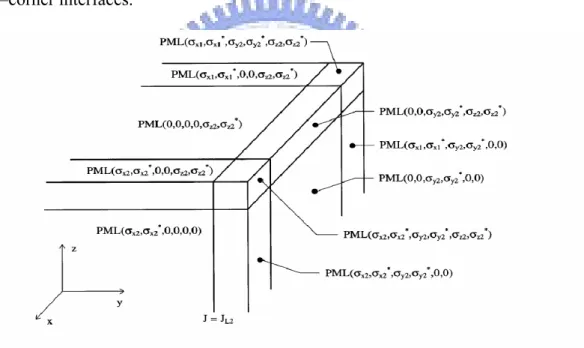
As we know that
σ σ
, *
control the wave attenuated, and the wave we use here are all transverse wave which the propagated direction is perpendicular to oscillated direction, that is why we divide the electric and magnetic field into two part, because if it propagated in one direction, then it may oscillated in one direction in a surface which is perpendicular in propagated direction, and the direction must have the other two vectors’ components. And we use the six PML broads enclose the simulation region, also we divide this region into six surfaces, twelve edges, and eight corners.In the six sides of the domain, the absorbing media are matched PML media of transverse conductivities equal to zero, for instance, media (0,0,0,0,σ σz, *)z in the upper and lower sides of the domain (Fig [3.3]). As a result, outgoing waves from the inner vacuum can penetrate without
28 reflection into these absorbing layers.
In the 12 edges, the conductivities are selected in such a way that the transverse conductivities are equal at the interfaces located between edge media and side media. This is obtained by means of two conductivities equal to zero and the other four equal to the conductivities of the adjacent side media, as shown in Fig 3.3. As a result, there is theoretically no reflection from the side–edge interfaces.
In the eight corners of the domain, the conductivities are chosen equal to those of the adjacent edges, so that the transverse conductivities are equal at the interfaces between edge layers and corner layers. So, the reflection equals zero from all the edge–corner interfaces.
For the condition that the PML thickness is not infinite, and the most outside is a perfect conductor, all we can do is divide the PML into many layers to attenuate the wave to zero.
From [22]. for a layer of thickness δ and longitudinal conductivity, ( )σ ρ
depending on the distanceρ from the interface, the apparent reflection is, as a function of the angle of incidence θ :
29 cos( ) 0 0
( ) [ (0)]
2
(0) exp[
( )
]
R
R
R
d
c
θ δθ
σ ρ ρ
ε
=
=
−
∫
And some numerical tests will be shown for various profiles of conductivity, parabolic conductivities as in [8], or conductivities increasing geometrically as in [9], this last profile being an optimum one to reduce the numerical reflection in wave–structure interaction problems. Details on the exact implementation of the conductivity at the mesh points can be found in [22, 23].
30
Chapter4: Simulation
In order to analysis the topography effect due to etch the trench in Phase-Shift Mask (PSM), we introduce FDTD to simulate the EM wave near the mask. For the reason that FDTD can compute the electric and magnetic filed in space domain for cartesian coordinates where divide the space into x,y,z’s direction Ex,Ey,Ez and Hx,Hy,Hz. And it can’t compute the phase, but only amplitude, so we use Solid-C to compute the phase and Aerial Image
4.1 Model of Simulation
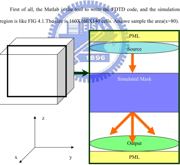
First of all, the Matlab is the tool to write the FDTD code, and the simulation region is like FIG 4.1.The size is 160X160X140 cells. And we sample the area(x=80).
First Step: As Ch3 mention the FDTD and PML, FDTD for EMW,PML for Simulated Mask Output PML PML Source z y x
31
absorbing the EMW. In order to reduce the memory space, so we just put Up and Down side PML. It also relate the source type as mention later.
Second Step: The source we use there is on axis which the EMW incidence normally into the object. The polarization here we choose the TE wave which Ez=0, and we choose Ex=1. The wavelength is 193nm, and the wave is the sinusoidal wave. Also, in order to reduce the memory space, we put the source generate form the mask. So the wavelength become to 126nm due to the mask index.
Third Step: Setting the mental index for FDTD. The mask we use here include Quartz(Qz) and Chromium(Cr), and the refractive index of Qz is 1.56+j1.38e-7,Cr is 0.84+j1.66. In order to get the permittivity ,conductivity ,permeability. We derive form Maxwell;s Equation:
The mental use here assume that relative permeability equal to 1.
Fourth Step: We choose three type 100nm(4X) contact hole to simulate.
0 0 0 0 2 2 2 2 0 2 2 2 2 0 0 ( ) * ' '' , 2 *, * ( ) , 2 2 , ( 1) r r r r r r r r r r r r r r r r r r r H J D E j E j j E j j N n jk N n k jnk j N N n k n k nk j jnk
σ
ε ε ϖ
σ
ε
ε ϖ
ε ϖ
σ
ε
ε
ε
ε
ε ϖ
σ
μ ε
μ ε
μ ε
ε ϖ
μ ε
ε
μ
ε ϖ
σ
μ
σ
ε ϖ
μ
μ
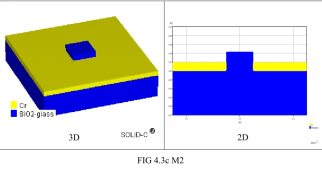
∇× = + = + = − = − = − = − = − − = = = − − = − = = = = (4-1)32 The first type is unetched for 0 degree.(M0) The second type is etched for 180 degree.( M1) The third type is also 180 degree(M2)
The mask structure we can view from figure below FIG 4.2a,b,c
® SOLID-C -0.2 0.0 0.2 X[痠] -0.10 -0.08 -0.06 -0.04 -0.02 0.00 0.02 0.04 0.06 0.08 0.10 Z[痠] SiO2-glass Cr FIG 4.2a M0 ® SOLID-C -0.2 0.0 0.2 X[痠] -0.10 -0.08 -0.06 -0.04 -0.02 0.00 0.02 0.04 0.06 0.08 0.10 Z[痠] SiO2-glass Cr FIG 4.2b M1 3D 3D 2D 2D
33 ® SOLID-C -0.2 0.0 0.2 X[痠] -0.10 -0.08 -0.06 -0.04 -0.02 0.00 0.02 0.04 0.06 0.08 0.10 Z[痠] SiO2-glass Cr FIG 4.3c M2
As the topography effect mention that the energy lose in the side wall for etched structure, so we create a structure like M2 which hope this structure can reduce energy lose in the 180 degree etched structure.
In the second part, we use Solid-C to simulate the Aerial Image. The simulation parameters and conditions are as follows:
Antireflective coating :ARC11(Refractive index:1.71−j0.43)(thickness:0.06um) Resist spin on: Positive CAR UV210(0.55um)
Refraction=1.72 A(1/mm)=0.0014 B(1/mm)=1.155 C(cm2/mJ)=0.0364
Defocus=0;Source:ArF(193nm)
Illumination system: Coherent=0.01(Pupil Shape: Circle); Polarization: TE Projection system: NA=0.75,Cricle Shape
Wafer stack structure is like the figure below
FIG 4.2 The mask type M0, M1, M2, blue region: Qz; yellow region: Cr
34 ® SOLID-C 0.0 X[痠] 0.0 0.2 0.4 0.6 Z[痠] Silicon ARC11 UV210
Under that condition, we can simulate the near field.
FIG 4.4a M0 near fileld
FIG 4.4b M1 near field
® SOLID-C -0.2 0.0 0.2 X [?] 0.30 0.25 0.20 0.15 0.10 0.05 0.00 -0.05 -0.10 Z [?]
Near Fields Phase [Rad.] Scale
-3.14020 -2.44225 -1.74430 -1.04634 -0.34839 0.34957 1.04752 1.74548 2.44343 ® SOLID-C -0.2 0.0 0.2 X [? ] 0.30 0.25 0.20 0.15 0.10 0.05 0.00 -0.05 -0.10 Z [? ]
Near Fields Transm. Scale
0.00000 0.65130 1.30260 1.95389 2.60519 3.25649 3.90779 4.55909 5.21039 ® SOLID-C -0.2 0.0 0.2 X [?] 0.30 0.25 0.20 0.15 0.10 0.05 0.00 -0.05 -0.10 Z [?]
Near Fields Phase [Rad.] Scale
-3.13902 -2.44122 -1.74342 -1.04563 -0.34783 0.34997 1.04776 1.74556 2.44336 ® SOLID-C -0.2 0.0 0.2 X [? ] 0.30 0.25 0.20 0.15 0.10 0.05 0.00 -0.05 -0.10 Z [? ]
Near Fields Transm. Scale
0.00000 0.36999 0.73998 1.10997 1.47995 1.84994 2.21993 2.58992 2.95991
FIG 4.3 Wafer stack film
Amp Phase
35
FIG 4.4c M2 near field
4.2 Simulation Result
From the Matlab simulation. We can get some data from that. First, we view the mask M0 and M1 and analysis them
20 40 60 80 100 120 140 160 20 40 60 80 100 120 140 j coordinate k c oo rdi nat e
Ex(i=iobs,j,k), time step = 400
-0.8 -0.6 -0.4 -0.2 0 0.2 0.4 0.6 0.8 ® SOLID-C -0.2 0.0 0.2 X [?] 0.30 0.25 0.20 0.15 0.10 0.05 0.00 -0.05 -0.10 Z [?]
Near Fields Phase [Rad.]
Scale -3.13854 -2.44078 -1.74301 -1.04525 -0.34748 0.35029 1.04805 1.74582 2.44358 ® SOLID-C -0.2 0.0 0.2 X [? ] 0.30 0.25 0.20 0.15 0.10 0.05 0.00 -0.05 -0.10 Z [? ]
Near Fields Transm.
Scale 0.00000 0.39798 0.79595 1.19393 1.59190 1.98988 2.38785 2.78583 3.18380
FIG 4.4 The near field amplitude and phase of the three type mask
Amp Phase
36
FIG 4.5a,b M0 and M1 in Ex field amplitude
As we can observe that the critical region, the right side is Air, left side is Qz. There is some scattering effect due to etched side wall, or some energy lose there. In the idea wave propagated, it must propagate into down side, but from this figure , we can observe that there are some wave propagating direction have horizontal direction. As we know that the wavelength is relate with the real part of the refractive index, as that parameter larger, the wave length is longer. For this reason, the wavelength in the air is 193nm, the wave length in the Qz is 126nm. Before going into the etched place, the waves are all propagate in one direction, and they all continues. But After propagating into the etched place, because the wavelengths of them are not the same. So there is a discontinuous area impact the wave propagating direction. So we assume that in the air-Qz interface, there are some wave propagated in horizontal direction. For this reason, we need to find the Poynting’s vector which means that the energy propagating direction to prove that there are some energy horizontally propagate.
20 40 60 80 100 120 140 160 20 40 60 80 100 120 140 j coordinate k c oo rdi nat e
Ex(i=iobs,j,k), time step = 400
-0.8 -0.6 -0.4 -0.2 0 0.2 0.4 0.6 0.8 (b) critical
37
(a) M0 in y-direction (b)M0 in z-dirction
(c)M1 in y-direction (d)M1 in z-direction FIG 4.6 Poynting vector(j=160,k=140)
As we use TE wave, and generate the wave which shake in +-x direction, so the weight of the x-direction is larger than any direction, and the magnetic field also smaller than the electric field. So the Poynting vector we can ignore some term. All we need to measure are the terms which multiply with Ex term. So we only need to consider the Py=-Ex*Hz, Pz=Ex*Hy.
In the Poynting vector, color red in y-direction means wave propagates to +y(right) direction, and color blue in y-direction means wave propagates to -y(left) direction. Color red in z-direction means wave propagates to +z(up) direction, and color blue in z-direction means wave propagates to -z(down) direction.
20 40 60 80 100 120 140 160 20 40 60 80 100 120 140 j coordinate k c oo rdi nat e
pz(i=iobs,j,k), time step = 400
-8 -6 -4 -2 0 2 4 6 8 x 10⁻⁴ 20 40 60 80 100 120 140 160 20 40 60 80 100 120 140 j coordinate k c oo rdi nat e
py(i=iobs,j,k), time step = 400
-8 -6 -4 -2 0 2 4 6 8 x 10⁻⁴ 20 40 60 80 100 120 140 160 20 40 60 80 100 120 140 j coordinate k co o rd in a te
pz(i=iobs,j,k), time step = 400
-8 -6 -4 -2 0 2 4 6 8 x 10⁻⁴ 20 40 60 80 100 120 140 160 20 40 60 80 100 120 140 j coordinate k co o rd in a te
py(i=iobs,j,k), time step = 400
-8 -6 -4 -2 0 2 4 6 8 x 10⁻⁴
38
In the FIG 4.6 Pz of M0 and M1 mask, we can observe that the waves propagate in –z direction. And the Py of M0 and M1. At first, the waves propagate center on the mid position, but when the position on the k=75,which M1 etched for 180 degree, the Py of M1 propagate to out direction, but they not center on like M0. So there is some energy lose here, so M1 can’t propagate energy as much as the M0. We think this is because the wavelength misfit due to the different index between air and Qz, so at the interface, the wave propagating direction is not –z direction, but it propagate horizontal direction.
And the FIG 4.7 is the cross section figure of Py in M1 structure(160x160). As we can observe the vertical direction is y-direction, and horizontal direction is x-direction. Color red means +y direction , color blue means –y direction. The mid square region is the etched place(filled air) for 180 degree phase difference(i=40 to 120;j=40 to 120). And we can observe that the wave like to propagate out direction, but not center on contact hole as FIG 4.7a,b,c. And FIG 4.7d, because it contact with Cr index, so it has less effect.
FIG 4.7a cross section of Py at k=70
20 40 60 80 100 120 140 160 20 40 60 80 100 120 140 160 i coordinate j c oor di nat e
py(i,j,70), time step = 400
-8 -6 -4 -2 0 2 4 6 8 x 10⁻⁴
39
FIG 4.7b cross section of Py at k=60
FIG 4.7c cross section of Py at k=50
20 40 60 80 100 120 140 160 20 40 60 80 100 120 140 160 i coordinate j c oor di nat e
py(i,j,50), time step = 400
-8 -6 -4 -2 0 2 4 6 8 x 10⁻⁴ 20 40 60 80 100 120 140 160 20 40 60 80 100 120 140 160 i coordinate j c oor di nat e
py(i,j,60), time step = 400
-8 -6 -4 -2 0 2 4 6 8 x 10⁻⁴
40
FIG 4.7d cross section of Py at k=40
For this reason, we use a mask structure like FIG 4.3c M2, and we analysis the energy lose between them. As front step, we use FDTD simulation, and in order let EMW more the same, so we put the Qz region and air region interface at k=40. So there are some different structures between them.
And the FIG 4.8 is the FDTD analysis and Poynting vector. This mask also generate 180 degree phase difference. And it is not etched, but it stick o
20 40 60 80 100 120 140 160 20 40 60 80 100 120 140 160 i coordinate j c oor di nat e
py(i,j,40), time step = 400
-8 -6 -4 -2 0 2 4 6 8 x 10⁻⁴
41
FIG 4.8a FDTD simulation
FIG 4.8b Poynting vector z-direction 20 40 60 80 100 120 140 160 20 40 60 80 100 120 140 j coordinate k c oor di nat e
pz(i=iobs,j,k), time step = 400
-8 -6 -4 -2 0 2 4 6 8 x 10⁻⁴ 20 40 60 80 100 120 140 160 20 40 60 80 100 120 140 j coordinate k c oor di nat e
Ex(i=iobs,j,k), time step = 400
-0.8 -0.6 -0.4 -0.2 0 0.2 0.4 0.6 0.8
42
FIG 4.8c Poynting vector y-direction
As we can observe from the FIG 4.8, we can see that the energy lose due index misfit reduce. In order to prove this experiment, so we need to compute the real energy before and after propagating though the contact hole. Due to the reason that FDTD have not phase term, but only amplitude term, so we need to compute a wavelength and square the amplitude. The formula is:
2 1
( )
(:,:, )
(:,:, )
5
_
k( )
k kIntensity k
ex
k
ex
k dxdx
dx
nm
Total
Intensity
Intensity k
=
=
×
=
=
∑
∑
∑
Which “:”means all term.
This is a discrete integral for FDTD. First we need to compute a region intensity, then we compute a wavelength where wavelength in air is 193nm, and in Qz is
20 40 60 80 100 120 140 160 20 40 60 80 100 120 140 j coordinate k c oor di nat e
py(i=iobs,j,k), time step = 400
-8 -6 -4 -2 0 2 4 6 8 x 10⁻⁴
FIG 4.8 FDTD Simulation and Poynting vector
43
126nm.The grid size is 5nm, so k2-k1=38 in air, k2-k1=25 in Qz.
And we divide these into 4 mode, Total(160x160) and part(80x80 for contact hole) region, and input(High side) and output(Low side). Mode1:Total input, mode2 part input, mode3 total output, mode4 part output. As the FIG 4.9. In order to compare the M0,M1,M2 energy transform.
1 2 3 4 0 .0 0 E + 0 0 0 2 .0 0 E -0 1 2 4 .0 0 E -0 1 2 6 .0 0 E -0 1 2 8 .0 0 E -0 1 2 1 .0 0 E -0 1 1 1 .2 0 E -0 1 1 1 .4 0 E -0 1 1 1 .6 0 E -0 1 1 One w a ve len g th inte nsi ty M o d e M 0 M 1 M 2
In the idea condition, the energy transmit is proportional to the open area. Take this simulation for example, Open area/Total area=1/9, so in the idea condition mode2/mode1=1/9, and the difference of the mode 3 and mode 4 is that mode include the energy inside the Cr which attenuated the EMW. Why the so mode3 is larger than the mode4 is sure. But why mode2 is smaller than the mode3 and mode4. This is because that the Poynting vectors are center on central region. Maybe the simulation region is too small, or we don’t add side wall PML so the waves reflect from side wall. As we can know that the structure M2 has larger energy transmit than M1, and more like to M0 which is unetched. And we use Solid-C to compute Aerial Image like to FIG 4.10, we can observe that the M0 and M2 are more closer than M0 and M1.
44 -0.15 -0.10 -0.05 0.00 0.05 0.10 0.15 0.00 0.05 0.10 0.15 0.20 0.25 Ae rial I m age Position M0 M1 M2
If we put there three structure in the same mask like the structure FIG 4.11a,b
a 3D
45 b 2D
c Near filed Amp
® SOLID-C -0.5 0.0 0.5 X [? ] 0.30 0.25 0.20 0.15 0.10 0.05 0.00 -0.05 -0.10 Z [? ]
Near Fields Transm.
Scale 0.00000 0.64737 1.29473 1.94210 2.58946 3.23683 3.88419 4.53156 5.17893 ® SOLID-C -0.2 0.0 0.2 X[? ] -0.1 0.0 0.1 0.2 0.3 0.4 0.5 Z[? ] SiO2-glass Cr
46
d Near field Phase
e Aerial Image on the wafer
® SOLID-C -0.2 0.0 0.2 X [? ] -0.15 -0.10 -0.05 0.00 0.05 0.10 0.15 Y [? ] norm. Intensity Scale 0.00002 0.02899 0.05796 0.08692 0.11589 0.14486 0.17383 0.20279 0.23176 ® SOLID-C -0.5 0.0 0.5 X [? ] 0.30 0.25 0.20 0.15 0.10 0.05 0.00 -0.05 -0.10 Z [? ]
Near Fields Phase [Rad.]
Scale -3.14149 -2.44339 -1.74530 -1.04720 -0.34911 0.34899 1.04708 1.74518 2.44327
47 -0.4 -0.3 -0.2 -0.1 0.0 0.1 0.2 0.3 0.4 -0.05 0.00 0.05 0.10 0.15 0.20 0.25 0.30 0.35 Aer ial Ima g e Position Rigorous Kirchhoff
f 1D Aerial image Rigorous compare to Kichhoff
As we can observe the figure, the Aerial Image in Rigorous(Thick mask) lowwer than Kichhoff(Thin mask), and in Rigorous M2 is like to M0 in Aerial Image, and M2 is larger than M1 structure. So M2 increase the intensity than M1.
And if we consider the alignment, we compare the two structure like FIG 4.12
FIG 4.12a 3D structure
48
FIG 4.12b 2D Aerial Image
-0.3 -0.2 -0.1 0.0 0.1 0.2 0.3 0.00 0.05 0.10 0.15 0.20 0.25 0.30 Ae ri al I m ag e Position
FIG 4.12c 1D Aerial Image
As we can observe that, if the mask isn’t alignment, the Aerial Image lose due to unalignment is small. ® SOLID-C -0.2 0.0 0.2 X [? ] -0.15 -0.10 -0.05 0.00 0.05 0.10 0.15 Y [? ] norm. Intensity Scale 0.00001 0.02849 0.05698 0.08546 0.11394 0.14242 0.17091 0.19939 0.22787
49
Chapter5: Conclusions
From the front chapter, we simulate the 3 type mask, and know that the energy lose in M1 which is etched due to the different medium of air and quartz. So in the interface there are some wave propagate to out direction. In order to solve this problem, we use another 180 degree contact hole to simulate. From the data present, we can see that the M2 structure has less side wall effect due to the no etched structure which behind the Cr, there is no air in the contact hole. And the difference of M2 and M1 in the medium interface is that: In the M1 structure, the energy in air and in the quartz are larger, and they all use the same source. So the scattering is larger. In the M2 structure, the energy in the air is less than the quartz, and the EMW in the air is from the quartz region, and after enter the Cr, much wave attenuate in the medium Cr. So the total energy in the air and quartz region is smaller than M1, from this reason, the wave scattering here is lower. And the Aerial Image in M2 is batter than M1.
50
Reference
[1] G. E. Moore, \Cramming more components onto integrated circuits," Electronics, vol. 38, No 8, pp. 114{117, April 19, 1965.
[2] A. K.-K. Wong, Resolution Enhancement Techniques in Optical Lithography, SPIE Press, 2001.
[3] Smith, B.W. and Sheats, J.R., eds., Microlithography: Science and Technology, ch. 3, Marcel Dekker, Inc., 1998
[4] M. Born and E. Wolf, Principles of Optics, Pergamon Press, 6th ed., 1987.
[5]Levenson, M. D. et al. “Improving resolution in photolithography with a phase-shifting mask.” IEEE Trans. Electron Devices 29, pp.1828-1836, 1982. [6]Terasawa, T. et al. “0.3 m optical lithography using a phase shifting mask.” Proc.
SPIE 1088, pp.25-33 ,1989.
[7]Matsuo, K. et al. “High resolution optical lithography system using oblique incidence illumination.” Technol. Digest IEDM 91, pp.70-972 ,1991
[8] H. Fukuda, A. Imai, and S. Okazaki, “Phase shifting mask and flex method for advanced photolithography,” Proc. of SPIE. vol. 1264, pp. 14- 25, 1990.
[9] H. Fukuda, A. Imai, and S. Okazaki, “Phase shifting mask and flex method for advanced photolithography,” Proc. of SPIE. vol. 1264, pp. 14- 25, 1990.
[10] Hiroshi Fukuda “Axial imaging Superposing (Super-FLEX) Effect Using the Mask
Modulation Method for in High-Numerical Aperture I-Line Lens”, Jpn. J. Appl. Phys. 30, 3037 ,1991.
[11] Shuo-Yen Choua and Jen-Chung Lou “Focus latitude enhancement of symmetrical phase mask design for deep submicron contact hole patterning” Department of Electronics Engineering and Institute of Electronics, National Chiao-Tung University, Hsinchu, Taiwan 30050, Republic of China
51
[12] M.S.C. Yeung. Modeling High Numerical Aperture Optical Lithography. In Proc.SPIE Optical/Laser Microlithography, vol. 922, pp. 149-167, 1988.
[13] Jaione Tirapu-Azpiroz and Eli Yablonovitch “Fast evaluation of Photomask Near-Fields in Sub-Wavelength 193nm Lithography”, Electrical Engineering Department, UCLA Los Angeles 90095-1594
[14] Goodman JW. Introduction to Fourier optics. San Francisco: McGraw-Hill Book Co.; 1968.
[15] K. S. YEE, “Numerical solution of initial boundary value problem involving Maxwell’s equation in isotropic media,” IEEE Trans. Antenna. Propag. 14, 302 (1966).
[16] J. P. Berenger. “A perfectly matched layer for the absorption of electromagnetic waves,” J. Compmfiona/ Physics, vol. 114, pp. 185200, 1994.
[17] J. P. Berenger. “Three-Dimensional Perfectly Matched Layer for the Absorption of Electromagnetic Waves,” J. Compmfiona/ Physics, 127, 363–379 (1996)
[18] David M . Hockanson “Perfectly Matched Layers Used as Absorbing Boundaries in a Three-dimensional FDTD code”TECHNICAL REPORT –UMR EMC LABORATORY
[19] Allen Taflove, Susan C. Hagness. “Computational Electrodynamics The Finite-Difference Time-Domain Method, 2nd
[20] Alfred K. Wong, Andrew R. Neureuther” Rigorous Three-Dimensional Time-Domain Finite-Difference Electromagnetic Simulation Finite-Difference Electromagnetic Simulation for Photolithographic Applications” IEEE TRANSACTIONS ON SEMICONDUCTOR MANUFACTURING, VOL. 8, NO. 4, NOVEMBER 1995
[21] 林振華 “電磁場與天線分析使用時域有差分法(FDTD) ” [22] J. P. Berenger, J. Comput. Phys. 114, 185 (1994).
52