四極射頻金氧半電晶體於雙埠量測下的去寄生效應方法與參數萃取之研究
85
0
0
全文
(2) Study of Two-port De-embedding Method for Four-Terminal RF MOSFET and Model Parameter Extraction. Student: Hung-Lin Lin. Advisor: Jyh-Chyurn Guo Tseung-Yuen Tseng. A Thesis Submitted to Institute of Electronics College of Electrical Engineering and Computer Science National Chiao Tung University in Partial Fulfillment of the Requirements for the Degree of Master in Electronics Engineering August 2005 Hsinchu, Taiwan, Republic of China.
(3) CMOS (sample layout) Source. Body. (model card) S. B. 4-Terminal(4T) model card. 4T. NMOS. 2-port Two-port. pad. RF. de-embedding 4T NMOS. 2-port. de-embedding. (Calibre-xRC). i.
(4)
(5) Study of Two-port De-embedding Method for Four-Terminal RF MOSFET and Model Parameter Extraction Student: Hung-Lin Lin. Adviser: Jyh-Chyurn Guo Tseung-Yuen Tseng. Department of Electronics Engineering and Institute of Electronics National Chiao Tung University. Abstract The fast development of wireless communication market increases the demand of electronic product. Under such a keen competition, CMOS transistor, which has the characteristics of low cost, high integration and low power, provides radio-frequency (RF) circuit designers an excellent choice. In the past, the Source and Body terminals of the MOS sample layout which foundries provide to customers are connected together. However it is not suitable for users. Therefore, foundries tend to provide 4-Terminal (4T) MOS sample layout to customers directly now.. In this thesis, 0.13 m process, 4T NMOS device is used for extraction but still put in 2-port pad to measure. This thesis includes a series of study and brings up a series of de-embedding and parameter extraction methods which are suitable for 4T NMOS under 2-port measurement.. This thesis utilizes software “Calibre-xRC” to calculate the interconnect capacitances coupling between device interconnect metals, and analyzes the capacitance variation to study the strategy of layout optimization. iii.
(6)
(7) Acknowledgment. v.
(8)
(9) Contents ....................................................................................................................i Abstract ...................................................................................................................iii Acknowledgment...................................................................................................... v Contents .................................................................................................................vii Figure Captions....................................................................................................... xi Chapter 1 Introduction............................................................................................ 1 1.1 Research Motivation..................................................................................... 1 1.2 Thesis Organization...................................................................................... 2 Chapter 2 Interconnect Capacitance....................................................................... 5 2.1 Introduction.................................................................................................. 5 2.2 Layout Analysis and Optimization Strategy .................................................. 6 2.2.1 Gate to Source Coupling Capacitance - Cgs_m ..................................... 7 2.2.2 Gate to Drain Coupling Capacitance - Cgd_m....................................... 8 2.2.3 Drain to Source Coupling Capacitance - Cds_m ................................... 8 2.3 Simulation result analysis ............................................................................. 8 2.3.1 Gate to Source Coupling Capacitance - Cgs_m ..................................... 9 2.3.2 Gate to Drain Coupling Capacitance - Cgd_m....................................... 9 2.3.3 Drain to Source Coupling Capacitance - Cds_m ................................... 9 2.4 Spacer Fringing Capacitance Analysis ........................................................ 10 2.4.1 Introduction ..................................................................................... 10 2.4.2 Measurement and simulation analysis .............................................. 12 Chapter 3 RF Measurement and De-embedding .................................................. 15 3.1 RF Measurement ........................................................................................ 15 vii.
(10) 3.1.1 Two-Port Scattering Parameters ....................................................... 16 3.1.2 RF Measurement Equipment............................................................ 18 3.2 Two-Port de-embedding ............................................................................. 18 3.2.1 Open pad de-embedding .................................................................. 19 3.2.2 Open, short pads de-embedding ....................................................... 21 3.2.3 Revised de-embedding method for our case ..................................... 23 3.3 Extraction of PAD parasitic resistance and inductance ................................ 27 Chapter 4 Model Parameters Extraction.............................................................. 29 4.1 Intrinsic Resistance .................................................................................... 29 4.1.1 Gate, Drain resistances extraction .................................................... 30 4.1.2 Source Resistance ............................................................................ 36 4.2 Intrinsic Capacitance .................................................................................. 37 4.2.1 Vds=0, Vgs>Vth ................................................................................. 37 4.2.2 Vds=1.2V, Vgs>Vth ............................................................................ 37 4.3 Substrate Model ......................................................................................... 38 4.4 Source Extrinsic Inductance ....................................................................... 45 Chapter 5 Experiment and Analysis ..................................................................... 47 5.1 Pad parasitic series resistance and inductance ............................................. 47 5.1.1 Inductance ....................................................................................... 47 5.1.2 Resistance........................................................................................ 48 5.2 Intrinsic resistance...................................................................................... 48 5.2.1 Gate, Drain resistances..................................................................... 48 5.2.2 Source resistance ............................................................................. 54 5.3 Intrinsic capacitance ................................................................................... 55 5.3.1 Vds=0, Vgs>Vth (average of 5GHz~15GHz) ...................................... 55 5.3.2 Vds=1.2V, Vgs>Vth ............................................................................ 57 viii.
(11) 5.4 Substrate Model ......................................................................................... 60 Chapter 6 Conclusion and Future Work............................................................... 65 6.1 RF De-embedding ...................................................................................... 65 6.2 Parameters Extraction................................................................................. 65 6.3 Substrate Model ......................................................................................... 66 Reference................................................................................................................ 69 Appendix ................................................................................................................ 71. ix.
(12)
(13) Figure Captions Chapter 2 Figure 2 - 1: the interconnect capacitance chart Figure 2 - 2: the cross-section view of NMOS before optimizing Figure 2 - 3: the cross-section view of NMOS after optimizing Chapter 3 Figure 3 - 1: illustration of RF measurement for a two-port system Figure 3 - 2: illustration of RF measurement for a two-port transistor Figure 3 - 3: the illustration of device with pad (S and B are connected) Figure 3 - 4: the equivalent circuit of device with pad Figure 3 - 5: the illustration of open pad layout Figure 3 - 6: the equivalent circuit of open pad Figure 3 - 7: the equivalent circuit of device with pad Figure 3 - 8: the illustration of short pad Figure 3 - 9: the equivalent circuit of short pad Figure 3 - 10: the illustration of de-embedding procedure Figure 3 - 11: the illustration of device with pad (S and B are separated) Figure 3 - 12: the equivalent circuit of device with pad (S and B are separated) Figure 3 - 13: the revised de-embedding procedure Chapter 4 Figure 4 - 1: channel RC transmission line Figure 4 - 2: the equivalent circuit of transistor with gsg pad Figure 4 - 3: the equivalent circuit after de-embedding Figure 4 - 4: the equivalent circuit of mos under Vgs>Vth and Vds=0. xi.
(14) Figure 4 - 5: the equivalent circuit of mos under Vgs>Vth and Vds=1.2V Figure 4 - 6: the equivalent circuit of mos under Vgs=Vds=0 Figure 4 - 7: illustration of Deep N-well in sectional drawing Figure 4 - 8: the equivalent circuit which is added Cdnw and Rdnw Figure 4 - 9: the equivalent circuit of NMOS under Vgs=Vds=0V Figure 4 - 10: the Rdnw, Cdnw fine-tuning extraction process Chapter 5 Figure 5 - 1: extracted RG of NF=18 NMOS under Vds=0, Vgs=0.5 and 1.2V Figure 5 - 2: extracted RG vs Vgs under Vds=0 Figure 5 - 3: extracted RD vs Vgs under Vds=0 Figure 5 - 4: extracted RG of NF=18 NMOS under Vds=1.2V, Vgs=0.5 and 1.2V Figure 5 - 5: simulation of Id and gm vs Vgs w/i and w/o Rs Figure 5 - 6: extracted Cgg of NF=72 NMOS under Vds=0 and Vgs=1.0V, 1.2V Figure 5 - 7: extracted Cgg of NF=18, 72 NMOS under Vds=1.2 and Vgs=1.2V Figure 5 - 8: extract Cgg at lower frequency (continue Fig.5-27) Figure 5 - 9: subtracted Rs effect first and extract Cgg at lower frequency (continue Fig.5-28) Figure 5 - 10: extract Rbulk initial value under Vds=Vgs=0 Figure 5 - 11: extract Cjd initial value under Vds=Vgs=0 Figure 5 - 12: measured and simulated Im(Y22)/ curves of NF=18 NMOS w/i Cdnw and Rdnw Figure 5 - 13: measured and simulated Im(Y22)/ curves of NF=36 NMOS w/i Cdnw and Rdnw Figure 5 - 14: measured and simulated Im(Y22)/ curves of NF=72 NMOS w/i Cdnw and Rdnw Chapter 6 Figure 6 - 1: 3-resistances substrate model. xii.
(15) Chapter 1 Introduction 1.1 Research Motivation With the rapid advancement of semiconductor technology, the size of transistor is scaled down aggressively to nanometer regime. Besides, because of the continuous expansion of wireless communication market, the demand of radio-frequency (RF) circuit products is increasing. In the view of circuit designers, under the consideration of high integration, low-cost of manufacture and low power, CMOS technology is an excellent choice. However, RF circuit designers usually meet a problem when designing their original circuit. When they proceed to simulate in advance, the simulated result and the measured result are always inconsistent. It means a feasible product needs to be built on the foundation of several tape-out fails. RF circuit designers have to rely on their intuition which is accumulated from experience, and fine tune their circuit and experience several times repeat tape-out to get a feasible product finally. But this kind of process will cost considerable and take much time. The reason that causes the mismatch of simulation and measurement is the inaccuracy of device model.. When a transistor is operated at radio-frequency, the parameters in original model are not enough to describe the transistor’s performance. For this reason, a practicable way is to put some external elements in original model equivalent circuit to make this expansive model equivalent circuit sufficient to describe real 1.
(16) performance of device. These external elements include Gate resistance (RG), Drain resistance (RD), Source resistance (RS), substrate components and some inductances and capacitances. We call them parasitic resistance, inductance, and capacitance.. The research motivation of this thesis is that we hope to build a reasonable model equivalent circuit. According to some numerical analysis, we can get the values of these parasitic components. Furthermore, we analyze these parasitic components physically, and explain their physical characteristics. Final, when the model is import to simulation software, the simulated result and measured result are coincident.. 1.2 Thesis Organization The theme of this thesis is the development of parasitic RLC extraction methods, the equivalent circuit analysis and verification for 4 terminals sub- m MOSFET.. In Chapter 2, I will introduce the influence of interconnect capacitance and how to minimize it by layout optimization. In Chapter 3 to Chapter 5, the extraction methods adopted in this study will be described. Some necessary modifications have been done to conform to our test-key in which the equivalent circuit, numerical analysis, and equation derivation will be provided. The extraction method is built and verified for 0.13 m RF CMOS technology.. It is continuous from Chapter 3 to Chapter 5. In Chapter3, I introduce the measurement set and explain the de-embedding methods. Besides, according to my specific consideration, there is some minor modification on the de-embedding method. 2.
(17) In Chapter 4, I elaborate every extraction method of each parameter I extract. It includes my consideration and revision to make the extraction suitable for my test-key. In Chapter 5, I demonstrate all extracted parameters and their curves from measured data. After that, I analyze their characteristics and bring up a new extraction method of Gate and Drain resistance. Finally, in Chapter 6, I explain the appropriate, reformed layout and extraction for next tape-out. This thesis can provide an extraction reference for others research workers.. 3.
(18)
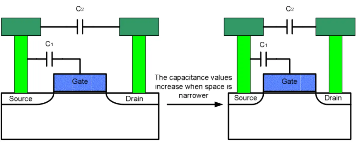
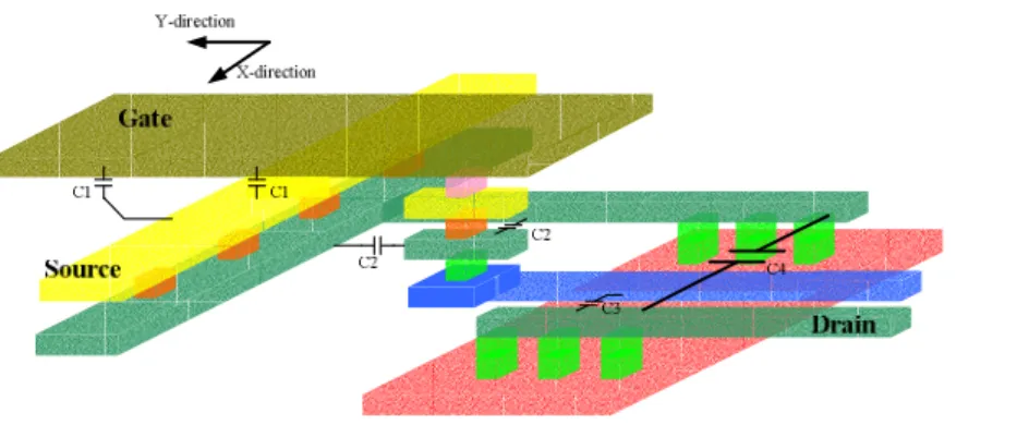
(19) Chapter 2 Interconnect Capacitance 2.1 Introduction A NMOS transistor is composed of p-substrate, n+ doped source and drain regions, n+ poly-Gate, and so on. A circuit designer will put the transistor in his circuit and use metal to connect it with other devices. Based on MOSFET layout analysis, we see that both metal-to-metal and metal to contact introduce interconnect coupling capacitances. Because they belong to device, they are more complicated to be analyzed and extracted than the general inter-metal coupling capacitance introduced by back-end process as pure interconnection lines.. If the transistor is not very small, and the circuit is not operated at very high frequency, these capacitances can be neglected because they are too small compared with intrinsic capacitances. However, if the transistor is very small, and the operating frequency is very high, these capacitances should not be neglected because of the small intrinsic capacitances and the small impedance across the interconnect capacitance. Please see Fig.2-1. (The impedance across capacitance is 1/ C). In this Chapter, I name the capacitance with a suffix “m”. It means the interconnect capacitance is coupled between metals inner device.. 5.
(20) Figure 2 - 1: the interconnect capacitance chart. These capacitances will affect the performance of MOS. For example, fT, the cut-off frequency, is a parameter to know how fast this transistor can operate. There is a rough formula can estimate fT: f T. gm when Cgs increase, fT decreases. Cgs Cgd. It shows the fact that when device is very small, interconnect capacitance will degrade the performance.. 2.2 Layout Analysis and Optimization Strategy Fig.2-2 and Fig.2-4 are the layout of NMOS transistor before and after layout optimization. Now I analyze their interconnect capacitance from the view of their structure to explain that after optimization, the interconnect capacitance effect decreases. The cross-section views of the layout before and after optimizing are showed in Fig.2-2 and Fig.2-3.. 6.
(21) Figure 2 - 2: the cross-section view of NMOS before optimizing. Figure 2 - 3: the cross-section view of NMOS after optimizing. 2.2.1 Gate to Source Coupling Capacitance - Cgs_m The gate to source coupling capacitance (Cgs_m) in Fig.2-2 is mainly contributed from the first element Gate-M3 and Source-M2 coupling and the second element from Gate-M1 and Source-M1 coupling. But, in Fig.2-3, the capacitance value decreases much because 1st: Source metal is stacked to M3, and connect to terminal in X-direction; 2nd: the Gate-poly terminator in Fig.2-3 is connect in U-shape. So the Gate-M3 doesn’t overlap Source metal. Besides, Gate-M1 and Source-M1 are staggered and separated in a distance. Such a layout design decrease the interconnect Cgs value.. 7.
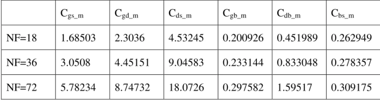
(22) 2.2.2 Gate to Drain Coupling Capacitance - Cgd_m Cgd_m value is contributed by Gate-poly and Drain-M1 coupling. Because the layout shape of Drain doesn’t change much, the Cgd_m values of Fig.2-2 and Fig.2-3 are closed. Because the space between Gate-poly and Drain-M1 in Fig.2-2 is wider than in Fig.2-3, Cgd value in Fig.2-3 is larger than in Fig.2-2.. 2.2.3 Drain to Source Coupling Capacitance - Cds_m Cds_m value is mainly contributed by Drain-M1 and Source-M1 coupling. When the transistor is smaller, the space between Drain-M1 and Source-M1 is narrower. And it explains that Cds_m value in Fig.2-3 is larger than in Fig.2-2.. 2.3 Simulation result analysis In section 2.2, Fig.2-3 layout is the optimized result of Fig.2-2 layout to reduce interconnecting coupling capacitance. To prove it, I use the software Calibre-xRC developed by Mentor-Graphic to calculate the coupling capacitance between different metals. Table 2-1 is the simulation result. The device used to be simulated is 0.13 m NMOS whose finger number is 18.. Unit: fF. Cgs_m. Cgd_m. Cds_m. Before optimize. 4.36988. 2.1651. 2.8203. After optimize. 1.68503. 2.3036. 4.53245. Table 2 - 1: the interconnect capacitance values of NMOS whose finger number is 18 (unit:fF). 8.
(23) According to Table 2-1, the Cgs_m value decreases much, Cgd_m value increases little and Cds_m value increases much.. 2.3.1 Gate to Source Coupling Capacitance - Cgs_m Compare Tab.2-2 and Tab.2-3, we can find that before layout optimizing, interconnect Cgs_m is mainly contributed by (1)Gate-M3 and Source-M2 overlap coupling and (2)Gate-M1 and Source-M1 sideward coupling. After layout optimizing, the overlap coupling and sideward coupling are eliminated or minimized. This layout design results in interconnect Cgs_m decreasing.. 2.3.2 Gate to Drain Coupling Capacitance - Cgd_m Drain layout shape is not changed after optimizing. The interconnect Cgd_m value is not changed much which is mainly contributed by Gate-poly and Source-M1 coupling.. 2.3.3 Drain to Source Coupling Capacitance - Cds_m Interconnect Cds_m is mainly contributed by Drain-M1 and Source-M1 sideward coupling. We hope the device size smaller, and then the space between Drain-M1 and Source-M1 will be narrower. Because device performance is not affected by Cds_m much, decrease in Cgs_m value is chosen first in the optimization work.. Besides, Table 2-4 is the simulated interconnect capacitance between every 9.
(24) terminal.. Cgs_m. Cgd_m. Cds_m. Cgb_m. Cdb_m. Cbs_m. NF=18. 1.68503. 2.3036. 4.53245. 0.200926. 0.451989. 0.262949. NF=36. 3.0508. 4.45151. 9.04583. 0.233144. 0.833048. 0.278357. NF=72. 5.78234. 8.74732. 18.0726. 0.297582. 1.59517. 0.309175. Table 2 - 2: simulated interconnect capacitance of each finger number NMOS (unit:fF). 2.4 Spacer Fringing Capacitance Analysis. 2.4.1 Introduction Not only the metal coupling capacitance, but also the capacitances between Gate-poly and Drain/Source diffusion region through spacer should not be neglected when the device is scaled down to nanometer level.. Please see the figure showed below left, C1 represents the coupling capacitance between Gate-poly and contact and C2 represents the coupling capacitance through spacer. When device is not very small, the space between Gate-poly and contact is wide and C1, C2 values are small relative to intrinsic Cgs. However, because fast development. of. the. semiconductor. technology, the device size has been extreme small and the space between Gate-poly and contact has been very narrow. Therefore, C1 and C2 values should not be neglected.. 10.
(25) However, there is not effective method to measure the values of these capacitances. De-embedding process at least removes the capacitance coupling higher than contact. The C1 and C2 in above figure are always included in extracted capacitance values. Nevertheless, we can calculate out these values by the 3-D simulation tools such as Raphael. We are not sure the accuracy of the simulated intrinsic capacitance which is coupling through the substrate. However we can simplify the device situation. We design a test-key, and the region under Poly-Gate is not channel but oxide. The cross-section view of the test-key is showed below left.. Of course it is not MOS transistor anymore but it simplify the situation of interconnect. coupling. because. semiconductor intrinsic capacitance is excluded. Because there must been a minimum space between diffusion active region and Poly-Gate, the coupling capacitance between Poly-Gate and contact and through spacer are not the same as mentioned formerly. In the above left figure, I use C1’ and C2’ to distinguish from former ones. Furthermore, C3 represents the coupling capacitance through the oxide under Poly-Gate.. We use RF measurement equipment to measure the s-parameters of the test-key and then extract Cgs, Cgd values from the measured data (About the RF measurement, it will be introduced in Chapter 3). In addition, we use the TCAD tool: Raphael to calculate the capacitance values. Here I name the calculated spacer capacitance with a suffix “sp”. If the measured capacitance values are close to simulated values, it means that the simulation tool: TCAD is reliable about the capacitance-in-oxide calculation. 11.
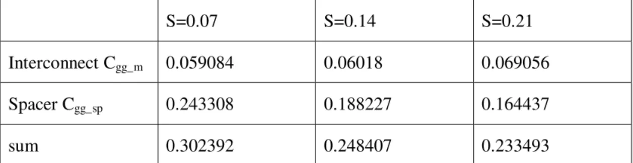
(26) (The materials of spacer are oxide, too). 2.4.2 Measurement and simulation analysis “S” in the Table 2-5 represents the distance from poly edge to active region edge. Because the region under Gate-poly is oxide, the equivalent circuit is quite simple. Therefore we can extract the capacitances from the formulas: Cgg. C gs. Cgd. Im( Y11 ). The extracted capacitances are showed in Table 2-5. S=0.07, NF=36. Cgg_sp=Cgs_sp+Cgd_sp 0.312986. S=0.14, NF=36. S=0.21, NF=36. 0.281111. 0.285417. Table 2 - 3: the extracted Cgg values of test-key (unit: fF/um). Besides, we build a device structure of test-key and import the source file to Raphael, and then simulating the sum of capacitance values which are coupled from Gate to Source and Gate to Drain.. Moreover, the extracted capacitances include interconnect capacitance because the open pad used for de-embedding just reserve the metals higher than M3. Therefore, the simulated interconnect capacitances should be added. Here I use the tool: Calibre-xRC to calculate the interconnect capacitance of the test-key. The simulated result is showed in Table.2-6.. 12.
(27) S=0.07. S=0.14. S=0.21. Interconnect Cgg_m. 0.059084. 0.06018. 0.069056. Spacer Cgg_sp. 0.243308. 0.188227. 0.164437. sum. 0.302392. 0.248407. 0.233493. Table 2 - 4: the simulated Cgg values of test-key (unit: fF/um). Comparing Table 2-5 and Table 2-6, we can find the simulated value and the measured values are close. This fact tells up that the simulation is believable and hence, the effects we analyze by the help of the tools such as interconnect capacitance and spacer capacitance are reliable.. 13.
(28)
(29) Chapter 3 RF Measurement and De-embedding 3.1 RF Measurement For the purpose of extracting MOS transistor parameters from measured data, on-chip RF measurement is adopted because of its accuracy. The data we get not only includes device’s performance but also the influence of the pad, coaxial cable and equipment. Before we put the die in the probe station, system calibration needs to be performed first to remove the influence of equipment, signal line and make the reference plane locates at the probe tips. (Fig.3-1). Figure 3 - 1: illustration of RF measurement for a two-port system. 15.
(30) 2-port system is adopted. (Please see Fig.3-2) It is because our measurement equipment (which will be mentioned in 3.1.2), system calibration technique and de-embedding method (which will be mentioned in 3.2) are mainly for 2-port measurement. We can still design a 4-port test patter to extract parameters, but the measurement system with special calibration techniques, and the de-embedding method are more complicated and not complete enough.. Figure 3 - 2: illustration of RF measurement for a two-port transistor. Typically speaking, the system calibration for on-wafer measurement is done by using a so-called impedance standard substrate (ISS) that can provide high-accuracy and. low-loss. standards. for. two-port. calibration. procedures. such. as. short-open-load-through (SOLT) and through-reflect-line (TRL). The SOLT calibration has been widely used because it is supported by virtually every VNA. [1]. 3.1.1 Two-Port Scattering Parameters. It is more suitable for two-port RF measurement to use scattering parameters 16.
(31) (s-parameters) to replace impedance and admittance parameters (z-, y-parameters). Because when device is operated at high frequency, it is quite difficult to provide adequate shorts or opens, particularly over a broad frequency range. Furthermore, active high-frequency circuits are frequently rather fussy about the impedance into which they operate, and may oscillate or even expire when terminated in open or short circuit. [2]. Please see the figure showed below, s-parameters defines input and output variables in terms of incident and reflected (scattered) voltage waves, rather than port voltage or current. Furthermore, the source and load termination are Z0.. b1 b2. s 11 s12 a1 s 21 s 22 a 2. where a1. E i1. Z0. a2. Ei 2. Z0. b1. E r1. Z0. b2. Er 2. Z0. and s11 s 21. b1 a1 b2 a1. s12. a2 0. E r1 Ei1. s 22. a2 0. Er 2 Ei1. b1 a2 b2 a2. a1 0. a1 0. Er 1 Ei 2 Er 2 Ei 2. The normalization by the square root of Z0 is a convenience that makes square of the magnitude of the various an and bn equal to the power of the corresponding 17.
(32) incident or reflected wave. s11 is simply the input reflection coefficient, s12 is the reverse transmission, s21 is a sort of gain and s22 is the output reflection coefficient. [2]. 3.1.2 RF Measurement Equipment. The figure showed below illustrates our setup of HF measurement system for on-wafer RF measurements. ICCAP is used to send the commands to instruments (Agilent E8364B PNA, and HP4142B) and the probing station is to perform the measurements for a specific DUT and to gather the measured data for extraction. [1]. 3.2 Two-Port de-embedding After system calibration is accomplished, the reference plane is located at the probe tips. However, the measured data still includes the pad effects which consist of capacitive, inductive and resistive effects. Our goal is to get the measured data of “pure” device. It is necessary to remove the parasitic effect of the pads including the metal line connecting signal pad and device. There are some techniques developed to remove these pad parasitic effect which is so-called de-embedding.. 18.
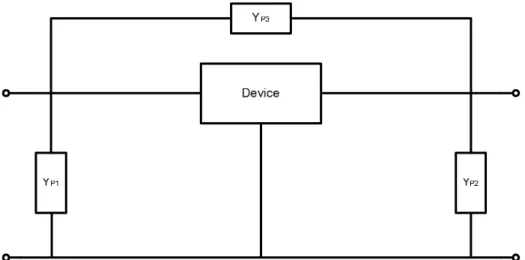
(33) 3.2.1 Open pad de-embedding. The most conventional and easiest method for obtaining the “pure” transistor’s measured data is to use an extra “open” pad.. When the transistor device is measured with the GSG pad, the layout is like Fig.3-3, the equivalent circuit is as Fig.3-4 and the open pad’s equivalent circuit is as Fig.3-5 and Fig.3-6.. Figure 3 - 3: the illustration of device with pad (S and B are connected). Figure 3 - 4: the equivalent circuit of device with pad. 19.
(34) Figure 3 - 5: the illustration of open pad layout. Figure 3 - 6: the equivalent circuit of open pad. After getting the measured s-parameters from device with pad and from open pad, we transform them to y-parameters and then we can get the transistor y-parameters by subtracting YP1, YP2 and YP3 from the measured data of transistor with pad. Theoretically, after this step, we get the pure measured data of transistor.. 20.
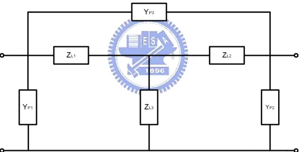
(35) We name the y-parameter of device with pad “Ymeas”, and the y-parameter of open dummy “Yopen”, and then. Yopen Ydut. YP1. YP 3 YP 3. Ymeas. YP 3 YP 2. YP 3. ( 3.1). Yopen. 3.2.2 Open, short pads de-embedding. The de-embedding method expounded in 3.2.1 has a defect that it neglects pad parasitic series effects of the connecting metal line. When device is very small, and operating frequency is very high, the resistive and inductive effect caused by the metal line should not be neglected. So it is necessary to use one more extra dummy pad such as “short” pad to remove the series parasitic components.. Under the considering of pad parasitic series effect, the equivalent circuit of device with GSG pad is as Fig.3-7. The short pad’s equivalent circuit is as Fig.3-8, Fig, 3-9.. Figure 3 - 7: the equivalent circuit of device with pad. 21.
(36) Figure 3 - 8: the illustration of short pad. Figure 3 - 9: the equivalent circuit of short pad. The first step is to get the YP1~YP3 value by measuring open pad and the method is mentioned in 3.2.1. After removing YP1~YP3, secondly, we have to remove ZL1~ZL3. We measure the s-parameters of short pad and transform it to y-parameter, and then use y-parameter matrix calculation to remove YP1, YP2 and YP3 in short pad. Finally, we transform all measured data to z-parameters and use z-parameter matrix 22.
(37) calculation to remove ZL1, ZL2 and ZL3 in the measured data of device with pad. Please see Fig.3-10 and the equations are showed below [3]. Yshort Y1 1 Ymeas Z dut. Yopen Z L1. Y1 Z L3. Z L3 Yopen Y2 1. Z L3 Z L2. Z L3. ( 3. 2). Y2 Y1 1. Figure 3 - 10: the illustration of de-embedding procedure. 3.2.3 Revised de-embedding method for our case. The de-embedding method mentioned in 3.2.1 and 3.2.2 is based on an important fact that the transistor is under 2-port GSG pad measurement. So, it is necessary to connect Source and Body together inter device and then connect to ground pad (Fig.3-3). However, 4-terminal (Gate, Drain, Source, and Body) MOS transistor is more practical to circuit designer because it is more flexible. They would 23.
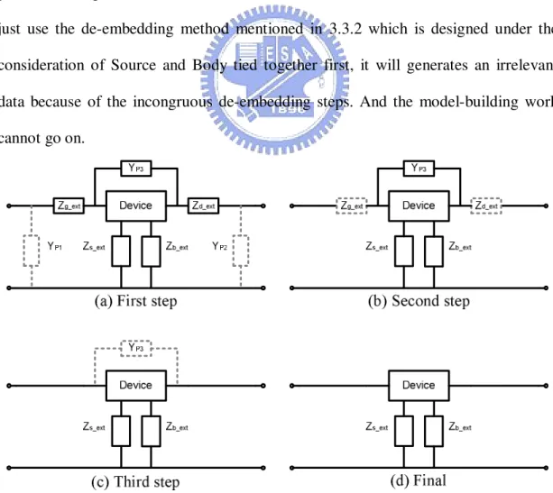
(38) like to connect Body terminals to ground line individually to make sure the pn-junction between p-substrate and n+ Drain in nMOS is under reverse-bias and prevent substrate affecting nMOS operation. And designer might bring into Body effect by connecting Body to other node except Source or ground to make his circuit fit specification.. Therefore, the latest sample layout which foundry provides to customers doesn’t connect Source and Body inter-device. We didn’t change the indigenous layout and connect the Gate, Drain to two individual signal pads and connect Source, Body to ground pads separately. (Fig.3-11). Figure 3 - 11: the illustration of device with pad (S and B are separated). Furthermore, 4-terminal transistor under 4-port RF measurement and corresponding system calibration, de-embedding methods are continuous developed, but not matured yet and will be very complicated expectedly.. Here I provide a revised de-embedding procedure which comes from my 24.
(39) practical measurement experience. And it is suitable for 4-terminal transistor but under 2-port GSG pad (Fig.3-11).. The equivalent circuit of measured device with pad is as Fig.3-12. I change the characters of the pad parasitic series components for later explanation. Zg_ext means the parasitic effect of the metal line connecting signal pad and Gate terminal of transistor and so do Zd_ext, Zb_ext, and Zs_ext. If the Source and Body are connected together first and then connect to ground pad, Zs_ext and Zb_ext are parallel and can be represented by ZL3 in Fig.3-7.. Figure 3 - 12: the equivalent circuit of device with pad (S and B are separated). First, I extract YP1, YP2, and YP3 from measured data of open pad (equation 3.1) and then subtract “just” YP1 and YP2 from measured data of device with pad (Fig.3-13 (a)).. Second, I extract Zg_ext and Zd_ext from measured data of short pad (equation 3.2) 25.
(40) and then subtract them from the data after first step (Fig.3-13(b)).. Third, subtract YP3 from the data after second step. The reason subtracting YP3 at last is the YP3 is almost capacitive and contributed by near metals which are located at the end of connecting metal line of port 1 and port 2. The original equivalent circuit shows that the nodes of YP3 are at the pad which contacts probe tip. It is not reasonable that they should be at the terminators of metal lines. So YP3 should be subtracted at last. (Fig.3-13). Although the metal lines connecting to Source and Body are retained, it is practicable to put external resistance or inductance to fit the measured curve. If we just use the de-embedding method mentioned in 3.3.2 which is designed under the consideration of Source and Body tied together first, it will generates an irrelevant data because of the incongruous de-embedding steps. And the model-building work cannot go on.. Figure 3 - 13: the revised de-embedding procedure. 26.
(41) 3.3 Extraction of PAD parasitic resistance and inductance The ZL1 and ZL2 in Fig.3-9 are regarded the same as Zg_ext and Zd_ext in Fig.3-12. However, each time you raise your probe and put down again to measure, the parasitic series resistances are different. The short pad de-embedding includes measured errors innately. But de-embedding procedure is still necessary because it at least decreases much pad effects from measured data of DUT. We can just observe the pad parasitic series resistance and inductance by the short pads.. The right above figure in Fig.3-10 shows that the short pad equivalent circuit subtracting YP1, YP2. And then ZL1 and ZL2 can be extracted from the formulas which are ZL1=Z11-Z12, ZL2=Z22-Z12. And then. Z L1. Z 11. Z 12. Z L2. Z 22. Z 12. R g _ ext. re(Z g _ ext ). re(Z L1 ), L g _ ext. R d _ ext. re(Z d _ ext ). re(Z L 2 ), L d _ ext. 27. im( Z g _ ext ). im( Z L1 ). im( Z d _ ext ). im( Z L 2 ). ( 3.3).
(42)
(43) Chapter 4 Model Parameters Extraction The extraction work is divided into two steps. First, extracting parameter values and second, using these values as initial values of each component in model equivalent circuit and fine-tuning them to make the simulated curves of equivalent circuit match the measured curves. In the first step, the substrate effect is neglected to simplify the equivalent circuit and make it easier to extract most parameters. I will extract intrinsic resistances and intrinsic capacitances in Vgs>Vth, Vds=0 or 1.2V and then extract substrate parameters in Vgs=Vds=0. Therefore, before second step, we will have many initial values of parameters including interconnect capacitances which are expounded in Chapter 2. There is one point noticeable: in first step, the path through junction capacitance Cjd is neglected because we ignore substrate effect, but the path through Cjs need to be handle carefully because the inductance Ls_ext makes the real part of the impedance see into node “ns” (Please see Fig.4-2) to ground is serious frequency-dependent [Appendix [a.3]].. 4.1 Intrinsic Resistance In Chapter 3, I explain the little revised de-embedding method I use. And I utilize short pad to extract the extrinsic resistances and inductances which result from the connecting metal line between Gate-port1 and Dran-port2. In this section, I will extract the resistances which belong to “intrinsic” transistor. These resistances are so-called intrinsic resistance. The extrinsic resistances have been removed after 29.
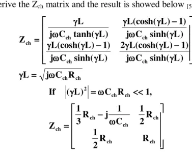
(44) de-embedding.. Basically, the intrinsic resistance is composed of two-parts: one is bias-independent which results from process materials such like Poly-silicon, salicide and the other is bias-dependent which results from channel characteristics.. 4.1.1 Gate, Drain resistances extraction 1. Vds=0, Vgs>Vth. Here I bring up a new method to extract the Gate and Drain bias-independent resistances. And then extract the channel resistance under Vds=0, Vgs>Vth. In BSIM model card, channel resistance is used to model non-quasi-static (NQS) effect which is a very important parameter when device is operated at high frequency. [4].. When a. MOS is operated at Vds=0 and Vgs>Vth, the channel is formed. If the operating frequency is very high, the region under the gate is like a distributed, uniform, resistance-capacitance (RC) transmission line.. Figure 4 - 1: channel RC transmission line. 30.
(45) In the Fig.4-1, Zch represents the two-port z-matrix of the channel which is a RC transmission line. The total capacitance under gate is Cch and the total resistance is Rch. We can derive the Zch matrix and the result is showed below [5]:. Z ch L. L j Cch tanh( L ) L(cosh( L ) 1) j C ch sinh( L ). L(cosh( L ) 1) j Cch sinh( L ) 2 L(cosh( L ) 1) j Cch sinh( L ). j C ch R ch. If Z ch. ( L)2. Cch R ch. 1 1 R ch j C ch 3 1 R ch 2. 1, 1 R ch 2 R ch. The assumption can be satisfied when the transistor length is very short and the channel opening is higher than 20% of the total channel height. It means that when Vgs is larger, the channel resistance will be smaller and this matrix is more appropriate [5].. Figure 4 - 2: the equivalent circuit of transistor with gsg pad. The Fig.4-2 represents the equivalent circuit of the device with the pad. The pad part is marked with orange color. On the one hand, the parasitic series resistances and inductances are named with suffix “ext”, on the other hand, the resistances belong to 31.
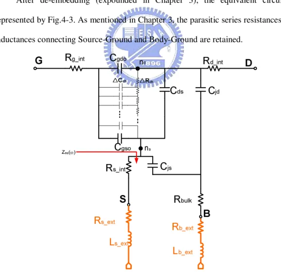
(46) device are named with suffix “int” such as Rg_int, Rd_int and Rs_int. Besides the channel transmission line, the capacitances coupled between Gate-Source, Gate-Drain, and Drain-Source are named “Cgso”, “Cgdo” and “Cds”. The suffix “o” means overlap. Because here we define channel capacitance Cch which is always categorized to Cgd and Cgs, the surplus Cgs and Cgd mainly come from overlap capacitances which are coupling through the overlap thin oxide. Therefore, for clear identification, I name the Gate-Drain and Gate-Source coupled capacitance “Cgdo” and “Cgso”. The junction capacitances between Drain-Substrate and Source-Substrate are represented by Cjd and Cjs. And the substrate is represented by a resistance “Rbulk”.. After de-embedding (expounded in Chapter 3), the equivalent circuit is represented by Fig.4-3. As mentioned in Chapter 3, the parasitic series resistances and inductances connecting Source-Ground and Body-Ground are retained.. Figure 4 - 3: the equivalent circuit after de-embedding. 32.
(47) Figure 4 - 4: the equivalent circuit of mos under Vgs>Vth and Vds=0. As previously mention, the path through Cjd is neglected temporarily but the impedance seen into “ns” to ground is not. This impedance is represented by Zns. According to the analysis [Appendix], the existence of Ls_ext will cause the real part of Zns serious frequency-dependent. The frequency-dependent components consist of Ls_ext, Rs_ext and Cjs. Besides, the imaginary part of Zns is approximate equal to. Ls.. Therefore, the equivalent circuit becomes as Fig.4-4 and the z-parameter is showed below which has been modified for our case: [5] R g _ int Z. 1 C ch 3C ds 3C gdo 1 1 Cch 2Cgdo R ch j Z ns ( ) R ch Z ns ( ) 3 C ch C gso C gdo (C ch C gso C gdo ) 2 C ch C gso C gdo 1 Cch 2C gdo R ch Z ns ( ) R d _ int R ch Z ns ( ) 2 C ch C gso C gdo. According to this matrix, I get an inspiration that we can eliminate the complex component Zns( )by Z11-Z12 and Z22-Z12. Because Vds=0, Cgso=Cgdo, the formulas become: 33.
(48) Re( Z 11. Z 12 ). R g _ int. 1 C ch 3. Re( Z 22. Z 12 ). R d _ int. R ch. 2C gdo. C gdo. C ch. 2C gdo. 3C ds. R ch. 1 C ch 2C gdo R ch 2 C ch C gso C gdo. 1 R ch 2 R d _ int. R g _ int. 1 R ch 6. 1 C gdo 3C ds R ch 3 C ch 2C gdo. 1 R ch 2. The two equations demonstrate a good thinking for us. Now taking Re(Z22-Z12) as example. According to the formulas, Re(Z22-Z12) can be divided into two parts: one is Drain resistance (Rd_int) which is gate-bias-independent and the other is half channel resistance which is gate-bias-dependent.. Re(Z11-Z12) is similar to Re(Z22-Z12) except another additional frequency dependent component. 1 C gdo 3Cds R ch . However, this component will be 3 Cch 2C gdo. explained in later Chapter 5 with measured data verification that this component is less than one-sixth Rch. Consequently, Re(Z11-Z12) is approximate equal to R g _ int. R ch . “ ” means a constant.. Following the thinking in last paragraph, when Vgs increases, the channel resistance decreases. The extracted Re(Z11-Z12) and Re(Z22-Z12) will approach to constant values, because the bias-dependent component (channel resistance) is reduced to minimum value even approaches to zero under high Vgs. Under this condition, the extracted Re(Z11-Z12) and Re(Z22-Z12) should only be Vgs-bias independent components which result from materials. Therefore, we can extract the bias-independent resistance under high Vgs. But we must be careful that do not give too high voltage in Gate otherwise the device will be damaged.. 2. Vds=1.2V, Vgs>Vth. 34.
(49) Figure 4 - 5: the equivalent circuit of mos under Vgs>Vth and Vds=1.2V. When the device is operated at saturation region (Vds=1.2V, Vgs>Vth), the equivalent circuit is Fig.4-5, and here we ignore the path through the junction capacitance Cjd temporarily. Zns( ) means the impedance seen into node “ns” to ground. Here the resistances are added suffix “sat” to distinguish from the resistance extracted under Vds=0 and Vgs<Vth (Fig.4-3), The components surrounded by dotted box are intrinsic components and can be represented by Yi parameters. Y11i Y12i. j (C gs. C gd ). j C gd. Y21i. gm. j C gd. Y22i. g ds. j (C ds. C gd ). And the z-parameters of the full equivalent circuit are [6]:. 35.
(50) ( Y22i ) * D ( Y11i ) * Z 22 R d _ sat Zns ( ) D i Y12 Z12 Z ns ( ) D i i i D Y11Y22 Y12Y21i Z11. R g _ sat. Z ns ( ). Here, the equivalent circuit and the z-parameters have been modified little for our case. And then the Gate and Drain resistance extraction equations can be derived: Ag. Re(Z 11. Z 12 ). R g _ sat. 2. Re(Z 22. Z 12 ). R d _ sat. 2. B. Ad B. If R g _ int. Re(Z 11. Z 12 ). R d _ int. Re(Z 22. Z 12 ). B Ag Ad. g m C gd C gs C ds. g ds (C gs C gs C gd. C ds g m C gd C gs C ds C gs C ds. C gd C ds. g ds (C gs. C gs C gd. C gs g m C gd. 2. C gd ). C gd C d s. g ds (C gs. C gs C gd. C gd ) 2. C gs C ds. g ds C gs C gd. C gd C ds. C gd ). C gd C ds. 2. 4.1.2 Source Resistance. Because of the existence of Ls_ext which causes some frequency dependent component in measured z-parameters, Source resistance is hard to be extracted from RF measured data. I extract source resistance from DC measurement.. Source resistance will cause gm degradation. According to fundamental electronics, we can derive this formula:. gm. g m0 1 R s gm0. (4.1). Because the Source and Body are not connected together first, the extracted 36.
(51) Source resistance includes the pad parasitic series resistance. (Rs=Rs_int+Rs_ext in Fig.4-2). 4.2 Intrinsic Capacitance. 4.2.1 Vds=0, Vgs>Vth. When Vds=0, Vgs>Vth, the equivalent circuit is like Fig.4-3. And the Z11-Z12 has been derived in section 4.1 which is: Z11 Z12. R g _ int. 1 Cch 2Cgdo R ch 2 Cch Cgso Cgdo. 1 Cch 3Cds 3Cgdo R ch 3 Cch Cgso Cgdo. According the equation, the imaginary part of Z11 is. j. (Cch. (Cch. 1 Cgso Cgdo ). 1 Cgso. Cgdo ). . So. we can extract the Cgg=Cch+Cgso+Cgdo value from Z11:. 1 Im( Z11. Cgg. (4.2). Z12 ). When Vds=0 and Vgs>Vth, the channel is formed. It is like a small conductor connecting Drain and Source. Therefore, Cch can be incorporated to Drain and Source. Here I define the Cgs and Cgd as:. Cgd. Cgdo. Cgs. Cgso. 1 1 Cgg Cch 2 2 1 1 Cch Cgg 2 2. 4.2.2 Vds=1.2V, Vgs>Vth. Under this bias situation, the transistor is operated at saturation region, and its equivalent circuit is showed in Fig.4-5. Cgg and Cgd are extracted from the formulas: C gd. Im( Y12 ). , C gg. Im( Y11 ). However, these extraction formulas are on a premise that after de-embedding, 37.
(52) the source resistance has been removed completely. In our case, there are two considerations. First: the Source parasitic series inductance is retained and make real part of Zns( ). increases with frequency. Second: although we can extract the. [appendix]. capacitance at lower frequency to reduce the frequency-dependent effect of real part of Zns( ), the real part of Zns( ), which is approximate to Source resistance at lower frequency, is not zero. When finger number of transistor increases, the gm value will increase and make the current flow through node “ns” increases. And then, the extracted Cgg and Cgd values are inaccurate.. So before extracting the capacitance value, I subtract the Source resistance first to make Vns closer to zero and extract at lower frequency for fear of the frequency-dependent effect of Re(Zns( )): Z. Rs. Rs. Rs. Rs. C gd. Z rev , Y rev. Im( Y12rev ). C gg. ( Z rev ) 1 , then. Im( Y11rev ). ( 4. 3 ). When transistor is operated at saturation region, Cgg is roughly equal to Cgs+Cgd, therefore, C gs. C gg. C gd. 4.3 Substrate Model Substrate model is very important for RF model. When the device is operated at high frequency, the impedance of the junction capacitance becomes very small. Therefore, substrate resistance will affect the small-signal output characteristics of the transistor because the small-signal in substrate will go through the junction capacitance to Drain. How to model the substrate effect accurately is an important issue. Here I adopt the model equivalent circuit showed in Fig.4-6. [7] 38.
(53) Figure 4 - 6: the equivalent circuit of mos under Vgs=Vds=0. When the transistor is operated at Vgs<Vth and Vds=0, the equivalent circuit is like Fig.4-6. The substrate is represented by Rbulk. Cjd, and Cjs. Cjd and Cjs are junction capacitances and Cgd0, Cgs0 represent gate-to-drain and gate-to-source capacitance. The suffix “0” means they are under zero Vgs bias. Cgb represents the sum of intrinsic and extrinsic gate-to-body capacitances. Because the device is operated at Vgs<Vth, most intrinsic components of the transistor are negligible. The Gate, Drain, and Source resistance are neglected here because the impedance of them is much smaller than the impedance of junction capacitance and substrate resistance [7].. After deriving the y-parameters of the equivalent circuit, we can get the extraction formulas: C gd 0 Im( Y11 ). (C gs 0. Im( Y12 ). Cgd 0. C gd 0. Re(Y22 ). 2. R bulk C 2jd. Im( Y22 ). (C gd 0 C jd ). Cgb ). C gb C jd R bulk. Im( Y12 ). C gs 0. Im( Y11 ) 2 Im( Y12 ) Im( Y22 ) Im( Y12 ). (4.4). Re( Y22 ) (Im( Y22 ) Im( Y12 )) 2. However, this extraction method doesn’t match our case because our test-key retains the pad parasitic series resistances and inductances in Source and Body 39.
(54) terminals. The existence of inductance will seriously affect the y-parameters. The extracted parameter curve is not stable with frequency. Nevertheless, this method still supports initial values of Cjd, Cjd and Rbulk for us. I extract the initial values under low frequency and then do some fine-tune work to make the simulated y-parameters curves of equivalent circuit fit the y-parameter curve of measured data.. According the NMOS layout, we can figure out the junction area between Drain or Source diffusion region and Substrate. And then we can derive one capacitance from another. According to the layout, the two-side diffusion regions are Source. Besides, the areas of the two-side diffusions are little larger than others. The Cjs can be calculated by the equation (0.73 and 0.42 are the edge length of the Drain region and two-side Source region. Please see the figure showed in the left side of next paragraph.):. C js. C jd. Source Area Drain Area. C jd. NF 1 2 ( NF 2. 0.73 0.42 NF 2. 2). ( 4. 5). There is one thing noticeable that the Cjs value should be smaller than the calculated result because one side of the diffusion region is oxide except substrate for the two-side diffusion region. Please see dotted circuit in left Figure. Therefore, this equation provides the initial value of Cjs from Cjd but we have to decrease little to fine-tune the curve.. Besides, the equivalent circuit in Fig.4-6 doesn’t include Cds which appears in other equivalent circuit. I think the Cds only comes from the interconnect capacitance. 40.
(55) Hence I use the value simulated by Calibre-xRC to represent Cds value. It has been demonstrated in Table 2-4 in Chapter 2.. During my fine-tune process, I find that if I add two additional components to the equivalent circuit of Fig.4-6, the simulated curves will fit measured curves better. These two components are one capacitance and one resistance in series. Moreover, this series resistance and capacitance are parallel with the substrate resistance (Rbulk of Fig.4-6).. I conjecture that these two components come from the Deep N-Well process which is for RF design to prevent noise going through substrate. When a circuit designer arranges his circuit layout, he can put N-well layer surrounding NMOS and then put a Deep N-well layer in rectangular shape which covers the inner edge of N-well “Ring”. And then, the N-well and deep N-well will be like a bowl and the p-substrate will be protected in it. The pick-up of the N-well is usually bias to the highest voltage to make the junction between p-substrate and n-well reverse-bias. This structure is designed to prevent outside noise into the p-substrate and affecting the performance of NMOS. The instruction of this structure is showed in Fig.4-7.. Figure 4 - 7: illustration of Deep N-well in sectional drawing. 41.
(56) Therefore, the additional capacitance results from the junction capacitance between N-well (including Deep N-well and sideward N-well) and p-substrate. I name it “Cdnw“. The additional resistance results from the impedance of the small-signal path in Deep N-well. I name it “Rdnw”. Please see Fig.4-8 as the more clear illustration.. Figure 4 - 8: the equivalent circuit which is added Cdnw and Rdnw. Although I do some fine-tune work, I am not aimless. There are two basic principles: first is getting the value under low frequency to minimum the retained inductive effect; second is following the simplified equivalent circuit for Y22 which is showed in Fig.4-10.. I explain my substrate model extraction steps for summarization: (1) Operating the transistor at Vgs=Vds=0 and the equivalent circuit is like Fig.4-9. (Rs_int and Rs_ext are summed up to Rs which extracted in section 4.1.2; Rb_ext, Ls_ext and Lb_ext results from our test-key situation which is mentioned in chapter 3; Moreover, Cdnw and Rdnw are added to the circuit.) (2) Extracting Cgs0 and Cgd0 and Cgb from the measured data according to equation 4.4. Because there is no current flowing into the node “ns”, the 42.
(57) results of revised extraction mentioned in section 4.2 is almost the same as un-revised. However we still extract capacitance from revised extraction method because the initial values of Rbulk and Cjd are extracted at low frequency too. (3) Rg_int and Rd_int are bias-independent because the channel doesn’t exist. Their values are extracted from Re(Z11-Z12) and Re(Z22-Z12) under Vds=0 and Vgs is large enough. (Please see the explanation in section 4.1.1.) (4) According to equation 4.4 and 4.5, and calculating the Rsub, Cjd and Cjs values. They will vary with frequency. Observing the curves, and take the values under lower frequency (about lower 3 GHz) as initial values for fine-tuning. (5) Extracting Ls_ext value according to equation 4.6. (This extraction will be explained in next 4.4.) Lb_ext is assumed equal to Ls_ext. (6) The Cds value comes from simulated interconnect Cds value which is discussed in chapter 2. (7) After steps (1) to (6), we now have all initial values of parameters in Fig.4-9 except Rdnw and Cdnw. Next, we build a circuit like Fig.4-9 in software: ADS and then simulating its y-parameters. After the calculating and fine-tuning parameters, we can get these parameters final. The calculating equation is showed in Fig.4-10. Basically, the parameters which don’t belong to substrate are not tuned.. 43.
(58) Figure 4 - 9: the equivalent circuit of NMOS under Vgs=Vds=0V. 1st : Y22. I2 V2. 2 nd : Y'22. V1 0. Y22. sC gd. 3 rd : Ysub ' (. 4th : Ysub 5th : Cdnw. Y'sub sCjs Im( Ysub ). 1 R bu lk , R dnw. 2. sC ds. 1 Y' 22. Cdn wR dnw j Cdnw 2 2 2 1 Cdn w R dnw (. 1 Im( Ysu b ). 1 ) Cdnw. 1/2. Cdnw. Figure 4 - 10: the Rdnw, Cdnw fine-tuning extraction process. 44. 1 ) sC jd. 1.
(59) 4.4 Source Extrinsic Inductance In Chapter 3, I expound the de-embedding procedure and mention that the pad parasitic series resistance and inductance are retained in the Source and Body terminals. In 3.3, I introduced that we can extract the pad parasitic series resistance and inductance of Gate and Drain terminals from Short and Open pads. To extract the pad parasitic inductance in Source terminal, we have to bias the device under Vgs>Vth and Vds=0 and the equivalent circuit is like Fig.4-3. To explain easier, here we can just use a small resistance Rch to replace the RC transmission line in Fig.4-3. And according to the analysis in Appendix [a.3], the real part of Zns( ) is serious frequency-dependent but the imaginary part of Zns( ) is approximate equal to Ls. If the finger number is larger, the Cjs value will be larger and it will make the approximation incredible. Therefore, I extract the Source extrinsic inductance from the measured data of NF=18 transistor and take the average of the imaginary part of Z12 at frequency=5GHz~40GHz.. The Z12 of Fig.4-3 which is mentioned in 4.1.1 is Z 12. Im( Z 12 ) Ls (1. 1 2C ch 2C gd R ch 2 C ch C gs C gd. Z ns ( ). Im( Z ns ( )) R s2C js 2. L s C js ) 2. 3. L2s C js 2. (R s. 3. 2 R bulk L s C 2js. R b ) 2 C 2js. 45. Ls. (4.6).
(60)
(61) Chapter 5 Experiment and Analysis 5.1 Pad parasitic series resistance and inductance Theoretically, after de-embedding, the pad parasitic effect can be removed. Actually, it is hard to achieve. However, it is still a very important procedure that de-embedding can remove some critical pad parasitic effect initially such as inductive and capacitive effects.. 5.1.1 Inductance. When operating frequency is very high, the thin metal line will behave as an inductance. We can extract the Gate, Drain parasitic series inductances from the short pad which subtracts the pad parasitic capacitive effect. It is mentioned in 3.3.. Besides, the source inductance extraction need to be extracted by the help of small channel resistance under Vgs>Vth and Vds=0. It is mentioned in 4.4.. The inductive effect becomes obvious when frequency is high enough. We take the average value of frequency=5GHz to 40GHz as the extracted parasitic inductance values. They are:. 47.
(62) Gate. Unit: pH. parasitic Drain. parasitic Source. inductance. inductance. inductance. 48.82. 47.39. 50.64. parasitic. Table 5 - 1: extracted parasitic inductance values. 5.1.2 Resistance. We take the average of the values at frequency=5GHz to 40GHz as the extracted parasitic resistance. They are:. Unit:. Gate parasitic resistance. Drain parasitic resistance. 1.14. 1.067. Table 5 - 2: extracted parasitic resistance values. 5.2 Intrinsic resistance According to the demonstration in section 4.1.1, the Gate and Drain resistance can be extracted from Re(Z11-Z12) and Re(Z22-Z12). They include two parts: bias-dependent and bias independent.. 5.2.1 Gate, Drain resistances 1. Vds=0, Vgs>Vth (average of 15GHz~30GHz). I name the extracted values of Re(Z11-Z12) and Re(Z22-Z12) “RG” and “RD”. First, we see the extraction curve of RG, (Fig.5-1). We can find that the curve is not 48.
(63) flat at lower frequency. It is because the extraction method expounded in 4.1.1 is under the situation that the channel is like a transmission line. If the frequency is not high enough, the RC delay in the channel is not obviously. Besides, although the channel resistance is small, and under this bias condition, we neglect the substrate effect, we have to sample the data carefully especially when extracting RD which will be influenced by Cjd easily. Therefore, I sample the data at 15GHz to 30GHz and take average as the extracted value. We can find the curves of Re(Z22-Z12) become unstable. RG. when the frequency is higher than 30GHz.. 70 65 60 55 50 45 40 35 30 25 20 15 10 5 0 -5. Vgs=0.5V. Vgs=1.2V. 0. 10G. 20G. Vgs=1.2. Vgs=0.5. 30G. 40G. Frequency. Figure 5 - 1: extracted RG of NF=18 NMOS under Vds=0, Vgs=0.5 and 1.2V. The extracted RG and RD values under Vgs>Vth and Vds=0 are showed in Table 5-3 and Table 5-4. Vgs. 0.5. 0.6. 0.7. 0.8. 0.9. 1.0. 1.1. 1.2. N18. -3.03. 0.448. 1.76. 2.37. 2.7. 2.92. 3.08. 3.21. N36. -0.978. 0.782. 1.38. 1.66. 1.81. 1.89. 1.98. 2.05. N72. -0.857. 0.244. 0.636. 0.744. 0.82. 0.866. 0.933. 1.07. Table 5 - 3: extracted RG values under Vds=0 (unit:. 49. ).
(64) Vgs. 0.5. 0.6. 0.7. 0.8. 0.9. 1.0. 1.1. 1.2. N18. 17.271. 9.771. 6.94. 5.603. 4.854. 4.39. 4.081. 3.866. N36. 8.4. 5.37. 4.07. 3.44. 3.12. 3.01. 2.88. 2.72. N72. 3.6. 1.86. 1.22. 0.907. 0.735. 0.628. 0.572. 0.574. Table 5 - 4: extracted RD values under Vds=0 (unit:. ). 4 NF=18 NF=36 NF=72. 3 2. RG. 1 0 -1 -2 -3 0.4. 0.5. 0.6. 0.7. 0.8. 0.9. 1.0. 1.1. 1.2. 1.3. Vgs. Figure 5 - 2: extracted RG vs Vgs under Vds=0. Now I plot the extracted RG figure according to Table 5-3 and show in above. Observing the curves, we can find the extracted values vary with Vgs. We take the equation mentioned in section 4.1.1: Re(Z11. Z12 ). R g _ int. 1 R ch 6. 1 Cgdo 3Cds R ch 3 Cch 2Cgdo. According to this equation, we can find the real part of Re(Z11-Z12) consists of two parts: a bias-independent resistance and a bias-dependent resistance associated with channel resistance. First we check the third component in the equation. Observing the extracted Cgg values under Vds=0, which are showed in later Table 5-8, 50.
(65) we can find when Vgs is higher than about 0.7V, the Cgg value approaches to a constant. In addition, the Cgdo value, which contributed by overlap and fringe capacitances, should be about one-third Cgd from experience, and under Vds=0, Cgd is equal to half Cgg, therefore, Cgdo is about one-sixth Cgg. Besides, Cds mainly results from interconnect capacitance and the simulated values have been showed in Table 2-4.. We take NF=72 NMOS as example. Its Cgg value under Vds=0, Vgs=1.2V is 431.1fF (later Table 5-9). The Cgdo value is about one-sixth Cgg and is 71.8fF. Cdsm of NF=72 NMOS is 18fF (former Table 2-4) Therefore, we can figure out that C gdo. 3Cds. Cch. 2Cgdo. is about 0.29. And then. 1 C gdo 3Cds R ch is less than one-sixth Rch 3 Cch 2C gdo. surely. It means that Re(Z11-Z12) is a constant “Rg_int” subtracting a value associated with channel resistance. When Vgs increases, channel resistance decreases. Therefore, the result of a constant subtracting a smaller value is larger than before. It explains the trend of the curves in Fig.5-2 reasonably.. Therefore we can utilize this phenomenon to extract the Poly-silicon resistance which is bias-independent component associated with the materials. We can bias Vgs carefully little higher than VDD and then the channel resistance reaches an extreme small value which can be neglected. And then Rg_int is equal to Re(Z11-Z12). 51.
(66) 18. NF=18 NF=36 NF=72. 16 14 12. RD. 10 8 6 4 2 0 0.4. 0.5. 0.6. 0.7. 0.8. 0.9. 1.0. 1.1. 1.2. 1.3. Vgs. Figure 5 - 3: extracted RD vs Vgs under Vds=0. The above Fig.5-3 is according to Table 5-4 which is the extracted RD plots varying with Vgs. First, the RD equation mentioned in section 4.1.1 is: Re(Z 22. Z 12 ). R d _ int. 1 R ch 2. According to this equation, we can explain the curves of Re(Z22-Z12) trend. When Vgs increases, channel resistance decreases. Therefore, the constant, Rd_int adds a smaller value and gets a smaller value than before. Base on the former discussion just elaborated, we can bias Vgs carefully little higher than VDD, and then get the intrinsic Drain resistance value which is just associated with the impedance in diffusion region.. This extraction brings two benefits. First, it can exclude the measured resistance error results from the contact between probe tip and pad. Because the contact condition of each time measurement is different, the extracted resistance is influenced by it each time. However, if we can extract the bias-independent component, it must 52.
(67) include the resistance results from the contact. And when we build a resistance model, we can subtract this component first. And then we can be sure the left resistance is associated with channel. Therefore, second, it makes the model more physical. Originally, we always get a large values need to be fit. Now we at least can build the resistance model as like “RG=Rg_int+R1(Vgs, )” and “RD=Rd_int+R2(Vgs, )” first. And then we start to model the channel performance as the parameter “R(Vgs, )”.. 2. Vds=1.2V, Vgs>Vth (average of 38.2GHz~40GHz). The RG extraction curves under Vds=0 and Vgs=0.5, 1.2V are showed in Fig.5-4. According to the extraction method expounded in 4.1.1, this method is reliable when the frequency is infinity. However, our measurement is limited by equipment and just up to 40GHz. But the curve is truly flatter when the frequency is higher. Here I sample the values at highest 10 frequency points which are 38.2 GHz to 40GHz.. 90. Vgs=0.5V. 80. Vgs=1.2V. 70 60. RG. 50 40 30. Vgs=0.5. 20 10. Vgs=1.2. 0. 10G. 20G. 30G. 40G. Frequency. Figure 5 - 4: extracted RG of NF=18 NMOS under Vds=1.2V, Vgs=0.5 and 1.2V. The extracted RG and RD values under Vgs>Vth and Vds=1.2V are showed in Table 5-6 and Table 5-7. 53.
(68) Vgs. 0.5. 0.6. 0.7. 0.8. 0.9. 1.0. 1.1. 1.2. N18. 16.498. 15.969. 15.353. 14.825. 14.337. 13.682. 13.38. 12.874. N36. 11.209. 11.156. 10.9. 10.615. 10.323. 10.017. 9.702. 9.366. N72. 5.511. 6.086. 5.94. 5.795. 5.648. 5.501. 5.312. 5.128. Table 5 - 5: extracted RG values under Vds=1.2V (unit:. ). Vgs. 0.5. 0.6. 0.7. 0.8. 0.9. 1.0. 1.1. 1.2. N18. 30.476. 28.296. 26.91. 26.092. 25.515. 25.021. 24.539. 24.024. N36. 14.935. 14.045. 13.547. 13.207. 12.947. 12.708. 12.455. 12.181. N72. 5.934. 5.487. 5.267. 5.117. 5. 4.891. 4.772. 4.652. Table 5 - 6: extracted RD values under Vds=1.2V (unit:. ). Although the curves really conform to the prediction mentioned in reference paper 4-3 and trend to constants, the substrate effect is still a latent problem. When Vds=0 and Vgs>Vth, the existence of channel resistance causes a small impedance path and then the path through Cjd is ignorable. However, when the transistor is operated at saturation region, the small channel resistance is replaced by a current source and an extreme large resistance. Under this situation, the impedance of the path through Cjd might not be ignorable.. 5.2.2 Source resistance. Following the extraction procedure mentioned in 4.1.2, the extracted Source resistances are showed in Table 5-8. Moreover, Fig.5-5 shows that Rs will causes Id and gm degradation. 54.
(69) Source resistance. NF=18. NF=36. NF=72. Unit:. 2.0798712. 2.079875. 2.30155. Table 5 - 7: extracted RS values from DC measurement (unit:. ). 60.0m w/o Rs Id w/i Rs Id w/o Rs gm w/i Rs gm. 50.0m. A or A/V. 40.0m 30.0m 20.0m 10.0m 0.0 0.0. 0.2. 0.4. 0.6. 0.8. 1.0. 1.2. Vgs. Figure 5 - 5: simulation of Id and gm vs Vgs w/i and w/o Rs. 5.3 Intrinsic capacitance. 5.3.1 Vds=0, Vgs>Vth (average of 5GHz~15GHz). The extracted Cgg curves under Vgs=1.0, 1.2V and Vds=0 of NF=72 transistors are showed in Fig.5-6. We observe that when the frequency increases, the curves become unstable. We have discussed in Chapter 4. In the first step of extraction work, we ignore substrate first which includes Cjd and Rbulk. (Because the Ls_ext exists, the Cjs is special to un-neglected. It is discussed in Appendix). Therefore, if the frequency is very high, the Cjd and Rbulk will start to affect the y-parameters or z-parameters.. 55.
(70) Besides, the Cgg will be extracted from the equation 4.2 in section 4.2.1. It. 1 Im( Z 11. is C gg. Z 12 ). Appendix [a.1] that is L. . This equation has to satisfy an assumption mentioned in. 2. R ch C ch. 1 . And when finger number is larger, Cch is. larger. Moreover, if the frequency is too high, the assumption is not established anymore and this equation cannot be used. Therefore, in Fig.5-6, the curve of NF=72 NMOS under high frequency becomes unstable.. 465.0f Vgs=1.0 V Vgs=1.2 V. 460.0f 455.0f. Cgg (F). 450.0f 445.0f 440.0f 435.0f 430.0f 425.0f. 0. 10G. 20G. 30G. 40G. Frequency. Figure 5 - 6: extracted Cgg of NF=72 NMOS under Vds=0 and Vgs=1.0V, 1.2V. Therefore, I take the average of. 1 Im( Z 11. Z 12 ). at frequency=5GHz~15GHz. as the Cgg values. The extracted Cgg values under different Vgs are showed in Table 5-8. Vgs. 0.5. 0.6. 0.7. 0.8. 0.9. 1.0. 1.1. 1.2. N18. 105.1. 109.6. 111.5. 112.2. 112.5. 112.4. 112.2. 111.9. N36. 206.6. 214.4. 217.9. 219.3. 219.7. 219.5. 219.1. 218.6. N72. 408.6. 423.8. 430.5. 433.4. 434.2. 434. 432.9. 431.1. Table 5 - 8: extracted Cgg values under Vds=0V (unit: fF). 56.
(71) The Cgs and Cgd are equal to half Cgg and the values are showed in Table 5-9.. Vgs. 0.5. 0.6. 0.7. 0.8. 0.9. 1.0. 1.1. 1.2. N18. 52.55. 54.8. 55.75. 56.1. 56.25. 56.2. 56.1. 55.95. N36. 103.3. 107.2. 108.95. 109.65. 109.85. 109.75. 109.55. 109.3. N72. 204.3. 211.9. 215.25. 216.7. 217.1. 217. 216.45. 215.55. Table 5 - 9: extracted Cgd values under Vds=0V (unit: fF). 5.3.2 Vds=1.2V, Vgs>Vth. There are two problems when extracting Cgg under Vds=1.2V and Vgs>Vth which has been mentioned in section 4.2.2 First, the imaginary part of Y11 is decreasing when frequency is increasing because the frequency-dependence of real part of Zns( ). Fig.5-7 is the extracted Cgg curves of NF=18, 72 transistors under Vgs=Vds=1.2V which are directly extracted from imaginary part of Y11 divided by . We can find that the curves are obviously decreasing when frequency is increasing. As mentioned in section 4.2.2, we can extract Cgg at lower frequency to make this bad effect minimum (Fig.5-8). Second, the imaginary part of Y11 is decreasing when the finger number of transistor is increasing because the more current flow into the node “ns” which is indicated in Fig.4-2, the node voltage is higher and causes the imaginary part of Y11 decreases. Therefore, even I extract Cgg under lower frequency as showed in Fig.5-8, the Cgg value of transistor whose finger number is 72 is not reasonable. It is not about 4 times of the Cgg value of transistor whose finger number is 18. Therefore, as mentioned in 4.2.2, I subtract Rs first from the measured z-parameters under low frequency and then transform it to y-parameters and use these y-parameters to extract 57.
(72) Cgg. Fig.5-9 is the result of revised extraction. We can find the Cgg values are reasonable. The Rs values are from the extraction result elaborated in Table 5-8 in section 5-2-2. The frequency range is 0.4GHz~2.2GHz, the first 10 frequency points except 0.2GHz. Cgd extraction has similar problem. Cgg and Cgd are extracted from equation 4.3 under 0.4GHz to 2.2GHz. The extracted Cgg, Cgd, and Cgs values under different Vgs bias are showed in Table 5-11, Table 5-12 and Table 5-13.. Vgs. 0.5. 0.6. 0.7. 0.8. 0.9. 1.0. 1.1. 1.2. N18. 94.82. 101.9. 106.1. 108.7. 110. 111.1. 111.7. 112.2. N36. 182.5. 194. 201.5. 205.8. 208.5. 210. 210.9. 211.4. N72. 366.4. 391.3. 409.6. 419.5. 424.2. 425.9. 425.9. 425.2. Table 5 - 10: extracted Cgg values under Vds=1.2V (unit: fF). Vgs. 0.5. 0.6. 0.7. 0.8. 0.9. 1.0. 1.1. 1.2. N18. 29.07. 29.15. 29.31. 29.55. 29.89. 30.23. 30.66. 31.13. N36. 57.06. 57.04. 57.38. 57.88. 58.52. 59.29. 60.2. 61.26. N72. 116. 116. 116.2. 117. 118.2. 119.7. 121.7. 124.1. Table 5 - 11: extracted Cgd values under Vds=1.2V (unit: fF). Vgs. 0.5. 0.6. 0.7. 0.8. 0.9. 1.0. 1.1. 1.2. N18. 65.75. 72.75. 76.79. 79.15. 80.11. 80.87. 81.04. 81.07. N36. 125.44. 136.96. 144.12. 147.92. 149.58. 150.71. 150.7. 150.14. N72. 250.4. 275.3. 293.4. 302.5. 306. 306.2. 304.2. 301.1. Table 5 - 12: extracted Cgs values under Vds=1.2V (unit: fF). 58.
(73) 350.0f NF=18 NF=72. 300.0f. Cgg (F). 250.0f 200.0f 150.0f 100.0f 50.0f. 0. 10G. 20G. 30G. 40G. Frequency. Figure 5 - 7: extracted Cgg of NF=18, 72 NMOS under Vds=1.2 and Vgs=1.2V. 350.0f 300.0f NF=18 NF=72. Cgg (F). 250.0f 200.0f 150.0f 100.0f 50.0f 0.0. 500.0M. 1.0G. 1.5G. 2.0G. 2.5G. Frequency. Figure 5 - 8: extract Cgg at lower frequency (continue Fig.5-27). 59.
(74) 450.0f 400.0f. NF=18 NF=72. Cgg (F). 350.0f 300.0f 250.0f 200.0f 150.0f 100.0f 50.0f 0.0. 500.0M. 1.0G. 1.5G. 2.0G. 2.5G. Frequency. Figure 5 - 9: subtracted Rs effect first and extract Cgg at lower frequency (continue Fig.5-28). 5.4 Substrate Model The equivalent circuit of NMOS under Vds=Vgs=0 has been showed in Fig.4-9. Cgg, Cgd0, and Cgb values of different finger number NMOS are extracted according to first two equations in equation 4.4. The curves are flat up to about 20GHz. If the frequency is higher, the y-parameter curve will behave the resonant effect especially when finger number is 72. I follow the former capacitance extraction sampling frequency range which is 0.4GHz to 2.2GHz. The extracted capacitance values are showed in Table 5-13. Cgg. Cgd0. Cgb. N18. 73.81. 31.05. 11.71. N36. 141.1. 61.26. 18.58. N72. 281.6. 125.2. 31.2. Table 5 - 13: extracted Cgg, Cgd0 and Cgb under Vds=Vgs=0. 60.
(75) Cjd and Rbulk initial values come from the last two equations in equation 4.4. Taking NF=36 NMOS as example. Please see Fig.5-10 and Fig.5-11. As I explained in section 4.3, because the retained Ls_ext and Rs, the Rbulk and Cjd extracted curves are not stable with frequency. However, when frequency is not very high, we can regard the impedance of inductance eliminated. Therefore, we can roughly sample the values in red dotted circuit as the initial values of Rbulk and Cjd. Moreover, Cjs is estimated from equation 4.4 but might be tuned smaller. 250 NF=36. initial case for Rbulk. 200. Sample Rbulk initial value 150 100 50 0 0. 10G. 20G. 30G. 40G. Frequency. Figure 5 - 10: extract Rbulk initial value under Vds=Vgs=0. 130.0f NF=36. initial case for Cjd fF. 120.0f. Sample the Cjd initial value. 110.0f 100.0f 90.0f 80.0f 70.0f. 0. 10G. 20G. 30G. 40G. Frequency. Figure 5 - 11: extract Cjd initial value under Vds=Vgs=0. 61.
(76) Besides, we refer to the values of Rs and Ls_ext, and estimate the values of pad extrinsic series resistance and inductance connecting to Body equal to 2ohm and 40pH, because the Body connecting metal is little wider then the Source connecting metal.. As I elaborated in section 4.3, the Rg_int, Rd_int, Rs, and Ls_ext are extracted from some methods. Here I omit the process. Now we get all parameters initial values except Cdnw and Rdnw. After fine-tune process which is showed in Fig.4-10, we can get the parameters showed in Table 5-14 and 5-15. Because the substrate effect influences the imaginary part of Y22 most, I fit im(Y22)/ im(Y22)/. first. Fig.5-12 to 5-14 are the. curves of measurement and simulation of the equivalent circuit model. showed in Fig.4-9 after adding the two new components “Rdnw” and “Cdnw”. The figures include NF=18, 36 and 72 NMOS.. Rg_int( ). Rd_int( ). Rs( ). Ls_ext(pH). Cgs(fF). Cgd(fF). Cgb(fF). Cds(fF). NF=18. 3.18. 5.04. 2.08. 55. 31.05. 31.05. 10.5. 4.53. NF=36. 2.08. 2.4. 2.08. 55. 61.26. 61.26. 18.58. 9.05. NF=72. 1.1. 1.2. 2.31. 55. 125.2. 125.2. 31.2. 18.07. Table 5 - 14: extracted parameters of Fig.4-9. Cjd(fF). Cjs(fF). Rbulk( ). Cdnw(fF). Rdnw( ). Rb_ext( ) Lb_ext(pH). NF=18. 52. 55. 230. 26. 240. 2.08. 40. NF=36. 105. 110. 120. 52. 120. 2.08. 40. NF=72. 200. 210. 70. 120. 50. 2.3. 40. Table 5 - 15: extracted parameters of Fig.4-9. 62.
(77) 90.0f measured simulation. 85.0f. Im(Y22)/. 80.0f 75.0f 70.0f 65.0f. 0. 10G. 20G. 30G. 40G. Frequency. Figure 5 - 12: measured and simulated Im(Y22)/ curves of NF=18 NMOS w/i Cdnw and Rdnw. 175.0f. measured simulation. 170.0f. Im(Y22)/. 165.0f 160.0f 155.0f 150.0f 145.0f 140.0f 135.0f. 0. 10G. 20G. 30G. 40G. Frequency. Figure 5 - 13: measured and simulated Im(Y22)/ curves of NF=36 NMOS w/i Cdnw and Rdnw. 350.0f measured simulation. 340.0f 330.0f. Im(Y22)/. 320.0f 310.0f 300.0f 290.0f 280.0f 270.0f. 0. 10G. 20G. 30G. 40G. Frequency. Figure 5 - 14: measured and simulated Im(Y22)/ curves of NF=72 NMOS w/i Cdnw and Rdnw. 63.
(78)
(79) Chapter 6 Conclusion and Future Work 6.1 RF De-embedding In Chapter 2, the interconnect capacitances are demonstrated by the help of software. In Chapter 3, the de-embedding methods to remove pad parasitic effects are discussed. The parasitic effect of pad “YP3” (Fig.3-12) is capacitive effect between two signal ports. The effect is mainly contributed by the interconnect capacitance. Moreover, when device is smaller, the capacitive effect between signal pad and ground pad which is contributed by interconnect capacitance will increase. Traditional open pad for de-embedding just retains metal layers higher than M3 (exclude M3) because the metals lower than M3 is categorized to “intrinsic” device.. To get the more “pure” intrinsic measured data of device, we can try to remove the interconnect capacitances after de-embedding. Nevertheless, although the de-embedding method can remove most pad parasitic effects to get more accurate pure device measured data, it will cost more dummy pads but not only open and short pads [9].. 6.2 Parameters Extraction After the extraction process elaborated in the thesis, we have two aspects of thinking. One is traditional 2-port RF measurement and the other is 4-port RF measurement. 65.
數據
+7
相關文件
Under the pressure of the modern era is often busy with work and financial resources, and sometimes not in fact do not want to clean up the environment, but in a full day of hard
Estimate the sufficient statistics of the complete data X given the observed data Y and current parameter values,. Maximize the X-likelihood associated
You are given the wavelength and total energy of a light pulse and asked to find the number of photons it
The learning and teaching in the Units of Work provides opportunities for students to work towards the development of the Level I, II and III Reading Skills.. The Units of Work also
Reading Task 6: Genre Structure and Language Features. • Now let’s look at how language features (e.g. sentence patterns) are connected to the structure
The research proposes a data oriented approach for choosing the type of clustering algorithms and a new cluster validity index for choosing their input parameters.. The
Wang, Solving pseudomonotone variational inequalities and pseudocon- vex optimization problems using the projection neural network, IEEE Transactions on Neural Networks 17
volume suppressed mass: (TeV) 2 /M P ∼ 10 −4 eV → mm range can be experimentally tested for any number of extra dimensions - Light U(1) gauge bosons: no derivative couplings. =>
