國 立 交 通 大 學
電信工程研究所
碩 士 論 文
新型低相位雜訊電流再利用四相位震盪器
之設計與研究
Design of the New Architecture for Low Phase Noise
Current-Reused Quadrature VCO
研究生:吳冠儀
指導教授:周復芳 博士
新型低相位雜訊電流再利用四相位震盪器
之設計與研究
Design of the New Architecture for Low Phase Noise
Current-Reused Quadrature VCO
研究生:吳冠儀 Student:Kuan-I Wu
指導教授:周復芳 博士 Advisor:Dr. Christina F. Jou
國 立 交 通 大 學
電 信 工 程 研 究 所
碩 士 論 文
A Thesis
Submitted to Institute of Communication Engineering
College of Electrical and Computer Engineering
National Chiao Tung University
in Partial Fulfillment of the Requirements
for the Degree of Master
in
Communication Engineering
June 2010
Hsinchu, Taiwan, Republic of China
新型低相位雜訊電流再利用四相位震盪器
之設計與研究
研究生:吳冠儀 指導教授:周復芳 博士 國立交通大學電信工程研究所碩士班 中 文 摘 要 本論文討論分為兩部分,其中各部分所提出電路之晶片製作皆由 TSMC 0.18μm mixed-signal/RF CMOS 1P6M 製程來實現。 第一部分為一個採用後閘極耦合 (Back-Gate Coupled)方式產生四相位輸出之電流 再利用震盪器。此四相位震盪器利用雙回授機制來達成改良型自發性轉移電導匹配 (Modified Spontaneous Transconductance Match, M-STM),可有效降低 NMOS 與 PMOS因製程變異對於轉移電導匹配上的影響,而可獲得更佳的輸出振幅平衡。根據量測結果 顯示:本 QVCO 震盪頻率為 4.84 - 5.17 GHz,在供應電壓為 1.3V 之條件下,功率損耗約 為 5.04mW,相位雜訊為 -117.4 dBc/Hz @ 1MHz,而 figure-of-merit (FOM)則為-184.07 dBc/Hz。 第二部分則提出一種新型的低雜訊電容耦合方式來完成注入鎖定,產生所需的四相 位 輸 出 訊 號 , 並 且 利 用 此 大 訊 號 弦 波 輸 出 來 達 成 尾 端 電 流 之 自 我 偏 壓 切 換 (Self-Switching Bias),這種新型態的電容耦合與尾端電流自我偏壓切換震盪器可以同時 達成低雜訊與低功率損耗的優點。根據量測結果顯示:本 QVCO 震盪頻率為 4.83-5.30 GHz,在供應電壓為 1.3V 之條件下,功率損耗約為 3.64mW,相位雜訊為 -125.8 dBc/Hz @ 1MHz,而 figure-of-merit (FOM)則為-193.87 dBc/Hz。
Design of the New Architecture for Low Phase Noise
Current-Reused Quadrature VCO
Student:Kuan-I Wu Advisor:Dr. Christina F. Jou
Department of Communication Engineering National Chiao Tung University
Abstract
This thesis consists of two parts. All the proposed circuits were implemented in TSMC 0.18μm mixed-signal/RF CMOS 1P6M technology.
Part I presents a back-gate coupled current-reused quadrature VCO (CR-QVCO) which use double feedback mechanism to accomplish modified spontaneous transconductance match
(M-STM) technique. This method is able to eliminate the transconductance difference
between NMOS and PMOS transistors so that high output amplitude balance can be achieved.
According to the measured results, the oscillation frequency is 4.84 - 5.17 GHz, and the
power consumption is about 5.04mW at the supply voltage of 1.3V. The phase noise at 1MHz
offset is -117.4dBc/Hz and the figure-of-merit (FOM) of the proposed QVCO is about
-184.07dBc/Hz.
Part II proposes a novel low noise capacitor-coupling method to perform injection locking, and therefore quadrature signals at the output can be obtained. Moreover, by using
these large signal sine-wave outputs to make the tail-current transistors self-switching, the
advantage of lower phase noise and lower power consumption can be simultaneously
achieved. According to the measured results, the oscillation frequency is 4.83 - 5.30 GHz, and
1MHz offset is -125.8 dBc/Hz and the figure-of-merit (FOM) of the proposed QVCO is about
Acknowledgement
本論文能夠順利的如期完成,首先要感謝我的指導教授周復芳博士,在這兩年多的 研究生涯中,周老師提供給我一個明確的研究方向,不厭其煩的給我鼓勵與細心的指導, 使我在研究領域上得到了不少寶貴的經驗,學會了用嚴謹的態度來做好每一件事情。同 時也要感謝交大電子所的陳巍仁教授與郭建男教授兩位口試委員撥空來參加口試,給予 我寶貴的意見,使得我的碩士論文能夠更加的完整。 在這裡我也要感謝所有實驗室的學長、同學、以及學弟妹們,兩年多以來的朝夕相 處,讓我從你們身上得到了很多寶貴的經驗與歡笑,首先是吳俊緯、林智鵬、吳匯儀、 沈宜星、江沛遠、蘇昭維、黃玠瑝、黃子哲、邱奕霖、林宗廷、黃哲揚、洪埜泰等諸位 學長的不吝指導,讓我獲益良多;另外也要感謝我的同窗好友柯漢宗、張傑翔、蘇國政 、李元袖、林子淵、陳佳聲、鄭漢維、吳卓諭、陳登政、李人維...等同學,在這兩年 多的研究生涯中與我一起奮鬥和努力。 最後要感謝我最愛的父親與母親,在求學的路上給予我最大的支持與呵護,讓我一 直擁有最好的學習環境。在此僅以小小的研究成果貢獻給我的家人,並與你們分享我的 喜悅。 吳冠儀 於 新竹交通大學 2010 年 夏Contents
Chinese Abstract ... I Abstract ... II Acknowledgement ... IV Contents... V List of Figures ... VII List of Tables ... XI
Chapter 1... 1
Introduction ... 1
-1.1 Background and Motivation ... 1
-1.2 Oscillator Fundamental ... 4
-1.3 Phase Noise ... 5
-1.4 Thesis Organization ... 18
Chapter 2... 19
CurrentReused Quadrature VCO with Modified Spontaneous Transconductance Match .... 19
-2.1 Introduction ... 19
-2.2 Circuit Design Consideration ... 28
-2.3 Chip Layout and Simulation Results ... 38
-2.4 Measurement Results and Discussion ... 41
Chapter 3... 49
CurrentReused Low Phase Noise Quadrature VCO with SelfSwitching Bias ... 49
-3.1 Introduction ... 49
-3.2 Circuit Design Consideration ... 55
-3.3 Chip Layout and Simulation Results ... 62
Conclusion and Future Work... 73
-4.1 Conclusion ... 73
-4.2 Future Work ... 74
Appendix A ... 75
Wideband CMOS DownConverting Mixer for WBand Receiver ... 75
-A.1 Introduction ... 75
-A.2 WideIFBandwidth Mixer Design ... 79
-A.3 Simulation and Measurement Results ... 87
-A.4 Conclusion and Future Work ... 93
-List of Figures
Fig. 1 - 1 Block diagram of PLL-based frequency synthesizer ... - 2 -
Fig. 1 - 2 DS-UWB spectrum allocation ... - 3 -
Fig. 1 - 3 Multi-band spectrum allocation ... - 3 -
Fig. 1 - 4 Block diagram of negative feedback systems ... - 4 -
Fig. 1 - 5 The phase noise per unit bandwidth ... - 5 -
Fig. 1 - 6 Limit-cycle due to amplitude restoring mechanism , [33] ... - 6 -
Fig. 1 - 7 A typical phase noise plot for a free running oscillator, [33] ... - 7 -
Fig. 1 - 8 Impulse response of an ideal LC oscillator, [33] ... - 7 -
Fig. 1 - 9 The equivalent system for ISF decomposition, [33] ... - 10 -
Fig. 1 - 10 Conversion of a low frequency sinusoidal current to phase, [33].... - 11 -
Fig. 1 - 11 Conversion of a tone in the vicinity of ωo, [33] ... - 11 -
Fig. 1 - 12 Conversion of circuit noise to excess phase, and then to phase-noise sideband ... - 13 -
Fig. 1 - 13 S( ) on a log-log axis, [33] ... - 15 -
Fig. 2 - 1 Examples of quadrature signal generation methods ... - 20 -
Fig. 2 - 2 Schematic of the conventional current-reused topology ... - 21 -
Fig. 2 - 3 Schematic of another conventional current-reused topology... - 22 -
Fig. 2 - 4 Schematic of the conventional parallel-coupled QVCO (P-QVCO) topology ... - 24 -
Fig. 2 - 5 Small signal equivalent circuit of the switching- and parallel-coupling transistor ... - 24 -
Fig. 2 - 6 Schematic of the conventional back-gate coupling QVCO ... - 26 -
Fig. 2 - 7 Small signal equivalent circuit of the back-gate-coupling transistor . - 26 - Fig. 2 - 8 Schematic of proposed current reused QVCO with modified STM .. - 28 -
Fig. 2 - 9 Proposed CR-QVCO operation during each half period ... - 29 -
Fig. 2 - 10 Concept of the proposed modified STM technique ... - 30 -
Fig. 2 - 11 Simulated output amplitude imbalance ratio of the proposed modified STM-QVCO ... - 32 -
Fig. 2 - 12 The M-STM mechanism to the ideal case of the proposed CR-QVCO . - 33 - Fig. 2 - 13 The M-STM mechanism to "Type 1 - Case 1" of the proposed CR-QVCO ... - 34 - Fig. 2 - 14 The M-STM mechanism to "Type 1 - Case 2" of the proposed
CR-QVCO ... - 35 -
Fig. 2 - 15 The M-STM mechanism to "Type 2 - Case 1" of the proposed CR-QVCO ... - 36 -
Fig. 2 - 16 The M-STM mechanism to "Type 2 - Case 2" of the proposed CR-QVCO ... - 37 -
Fig. 2 - 17 Chip layout of the proposed modified STM-QVCO... - 38 -
Fig. 2 - 18 Simulated phase noise of the proposed modified STM-QVCO... - 39 -
Fig. 2 - 19 Simulated tuning range of the proposed modified STM-QVCO ... - 39 -
Fig. 2 - 20 Bias-Tee Model ... - 41 -
Fig. 2 - 21 Signal Source Analyzer (Agilent E5052B) ... - 42 -
Fig. 2 - 22 Digital Signal Analyzer (Agilent DSA91204A) ... - 42 -
Fig. 2 - 23 Chip photo of the proposed modified STM-QVCO ... - 43 -
Fig. 2 - 24 Arrangement of DC and RF probes ... - 44 -
Fig. 2 - 25 Photograph of the probe station ... - 44 -
Fig. 2 - 26 Measured phase noise of the proposed modified STM-QVCO ... - 45 -
Fig. 2 - 27 Measured output spectrum of the proposed modified STM-QVCO - 45 - Fig. 2 - 28 Measured tuning range of the proposed modified STM-QVCO ... - 46 -
Fig. 2 - 29 Measured output waveform of the proposed modified STM-QVCO - 46 - Fig. 2 - 30 Measured output amplitude imbalance ratio of the proposed modified STM-QVCO ... - 47 -
Fig. 3 - 1 Schematic of the conventional parallel-coupled QVCO (P-QVCO) . - 50 - Fig. 3 - 2 Schematic of the conventional top series-coupled QVCO (TS-QVCO) .. - 51 - Fig. 3 - 3 Schematic of the conventional bottom series-coupled QVCO (BS-QVCO) ... - 51 -
Fig. 3 - 4 Schematic of the conventional middle series-coupled QVCO (MS-QVCO) ... - 52 -
Fig. 3 - 5 Varying VGS cycles a MOS transistor between "on" and "off" ... - 53 -
Fig. 3 - 6 Schematic of the conventional self-switching biased QVCO ... - 54 -
Fig. 3 - 7 Schematic of the proposed self-switching biased QVCO ... - 55 -
Fig. 3 - 8 Novel injection method of the proposed self-switching biased QVCO .... - 56 - Fig. 3 - 9 State-1 of the proposed self-switching biased QVCO ... - 58 -
Fig. 3 - 10 State-2 of the proposed self-switching biased QVCO ... - 58 -
Fig. 3 - 11 State-3 of the proposed self-switching biased QVCO ... - 59 -
Fig. 3 - 13 Simulated currents in the current-limited regime ... - 60 -
Fig. 3 - 14 Simulated currents in the voltage-limited regime ... - 60 -
Fig. 3 - 15 The definitions of current-flow used in Fig. 3 - 13 and Fig. 3 - 14 . - 61 - Fig. 3 - 16 Chip layout of the proposed self-switching biased QVCO ... - 62 -
Fig. 3 - 17 Simulated phase noise of the proposed self-switching biased QVCO .... - 63 - Fig. 3 - 18 Simulated tuning range of the proposed self-switching biased QVCO .. - 63 - Fig. 3 - 19 Bias-Tee Model ... - 65 -
Fig. 3 - 20 Signal Source Analyzer (Agilent E5052B) ... - 66 -
Fig. 3 - 21 Digital Signal Analyzer (Agilent DSA91204A) ... - 66 -
Fig. 3 - 22 Chip photo of the proposed self-switching biased CR-QVCO ... - 67 -
Fig. 3 - 23 Arrangement of DC and RF probes ... - 68 -
Fig. 3 - 24 Photograph of the probe station ... - 68 -
Fig. 3 - 25 Measured phase noise of the proposed self-switching biased QVCO at f o= 4.83GHz ... - 69 -
Fig. 3 - 26 Measured phase noise of the proposed self-switching biased QVCO at f o= 5.29GHz ... - 69 -
Fig. 3 - 27 Measured output spectrum of the proposed self-switching biased QVCO ... - 70 -
Fig. 3 - 28 Measured tuning range of the proposed self-switching biased QVCO... - 70 - Fig. 3 - 29 Measured output waveform of the proposed self-switching biased QVCO ... - 71 -
Fig. A - 1 Conventional double balanced mixer ... - 75 -
Fig. A - 2 Conventional double balanced mixer with gain-enhancement ... - 76 -
Fig. A - 3 Schematic of the wideband receiver ... - 77 -
Fig. A - 4 Schematic of the wide-IF-bandwidth mixer ... - 79 -
Fig. A - 5 Schematic of the input RF circuit ... - 80 -
Fig. A - 6 Vertical view of the Marchand balun [37], [38] ... - 81 -
Fig. A - 7 Lateral view of the Marchand balun [37], [38] ... - 81 -
Fig. A - 8 Simulated magnitude error of the Marchand balun ... - 82 -
Fig. A - 9 Simulated phase error of the Marchand balun ... - 82 -
Fig. A - 10 Simulated insertion loss of the Marchand balun ... - 83 -
Fig. A - 11 Simulated return loss of the Marchand balun ... - 83 -
Fig. A - 12 Schematic of the mixer core ... - 84 -
Fig. A - 14 CMRR of the output IF circuit ... - 86 -
Fig. A - 15 Chip layout of the proposed wide-IF band mixer ... - 87 -
Fig. A - 16 Chip photo of the proposed wide-IF band mixer ... - 88 -
Fig. A - 17 Arrangement of DC and RF probes ... - 89 -
Fig. A - 18 Photograph of the probe station ... - 89 -
Fig. A - 19 Photograph of the measurement environment in Chip Implementation Center ... - 90 -
Fig. A - 20 RF port return loss for RF signal from 8.7-17.4 GHz ... - 91 -
Fig. A - 21 IF port return loss for IF equals to DC-8.7 GHz ... - 91 -
Fig. A - 22 Conversion gain versus RF frequency with LO fixed at 17.4 GHz - 92 - Fig. A - 23 Schematic of the frequency doubler ... - 93 -
Fig. A - 24 Schematic of the constant-gm bias circuit ... - 94 -
Fig. A - 25 Chip Layout of the proposed wide-IF band mixer with LO frequency doubler ... - 94 -
List of Tables
Table 1 - 1 Wireless communication system characteristic ... - 2 -
Table 2 - 1 Simulated results of the proposed modified STM-QVCO ... - 40 -
Table 2 - 2 Comparison of QVCO Performance ... - 48 -
Table 3 - 1 Simulated results of the proposed modified STM-QVCO ... - 64 -
Table 3 - 2 Comparison of QVCO Performance ... - 72 -
Chapter 1
Introduction
1.1
Background and Motivation
As increasing demand for personal wireless communications, the requirements of
low-cost and low-power for wireless system have dramatically increased. Compact circuits,
with minimum area, are required to reduce the equipment size and cost. Thus, we need a very
high degree of integration, if possible a transceiver on a chip, either without or with a reduced
number of external component. In addition to area and cost, it is very important to reduce the
voltage supply and the power consumption. Wireless transceivers for many standards,
including GSM, Bluetooth, WLAN, and Wireless Personal Area Network (WPAN) require
low-power design techniques to enhance their battery lifetime and to improve their portability.
At the same time, the development of advanced CMOS technology with the shrunk channel
length is achieving higher cut-off frequency. Instead of bipolar and GaAs (Gallium Arsenide),
CMOS is very attractive for RFIC due to the ability of system-on-chip (SOC) implementation.
In addition to this benefit, scaling CMOS technology also satisfies the requirement of reduced
cost and smaller size.
In the wireless transceiver blocks, phase-locked loops (PLL) are widely utilized such as
frequency synthesizers, as shown in Fig. 1 - 1. Since the voltage-controlled oscillators (VCO)
play a key role in the PLL circuits and the phase noise of the VCO directly affect the
Table 1 - 1 Wireless communication system characteristic
Fig. 1 - 1 Block diagram of PLL-based frequency synthesizer
Due to the requirements of quadrature local oscillator (LO) generation for up-conversions and
down-conversions with image-reject mixing in wireless transceiver blocks, a quadrature VCO
(QVCO) with quadra-phase outputs is a general design.
In 2002, the Federal Communications Commission (FCC) has allocated 7500 MHz of
spectrum for ultra-wideband (UWB) system in 3.1~10.6 GHz frequency range [1]. According
when center frequency is over than 2.5GHz, or has a fractional bandwidth is equal to or greater
than 20% of the center frequency when the center frequency is less than 2.5GHz. There are two
proposals for UWB system: DS-CDMA (Direct-Sequence Code Division Multiplexing Access)
and MB-OFDM (Multi-Band Orthogonal Frequency Division Multiplexing).
DS-CDMA uses a sequence of Gaussian monocycle pulses which their spectrum is spread
as in Fig. 1 - 2. The lower band occupies the spectrum from 3.1 to 4.85 GHz and the upper band
occupies the spectrum from 6.2 to 9.7 GHz [2]. The 5-6 GHz band is dedicated to WLAN
802.11a systems.
In MB-OFDM UWB, see Fig. 1 - 3, frequency span is grouped into five major band groups
which are in turn sub-divided into 14 bands in total, each band is 528 MHz bandwidth [3] .
Fig. 1 - 2 DS-UWB spectrum allocation
1.2
Oscillator Fundamental
Fig. 1 - 4 Block diagram of negative feedback systems
In spite of oscillators are nonlinear in nature, they are usually viewed as a linear
time-invariant feedback system as shown in Fig. 1 - 4. Although we can easily write the two
block diagram, which are a gain block and a feedback block, to describe the negative
feedback system, the main design issues are in the details of how these two circuits interact
and how this interaction cause oscillation to occur. In the s-domain, the transfer function of this
negative feedback system is given by
( ) ( ) 1 ( ) ( ) out in V A s s V A s F s (1. 1)
The denominator of the transfer function goes to zero when the loop gain A(s)F(s) is
equal to –1 at a specific frequency ωo, implying that there is an output without a driving input
signal, just what is needed for an oscillator. This is the well-known "Barkhausen criteria" and
they allow the circuit designer to look at the amplifier and feedback blocks to determine the
1.3
Phase Noise
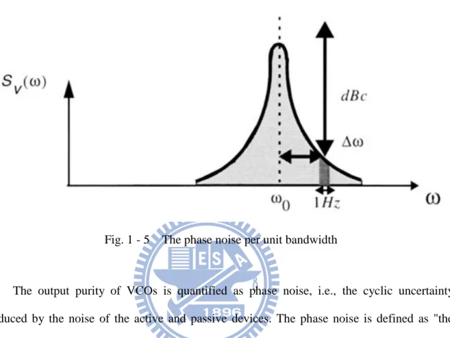
Fig. 1 - 5 The phase noise per unit bandwidth
The output purity of VCOs is quantified as phase noise, i.e., the cyclic uncertainty
induced by the noise of the active and passive devices. The phase noise is defined as "the
relative noise power per unit bandwidth at certain offset with respect to the carrier power".
That is,
( , 1 ) 1 0 l o gs i d e b a n d o t o t a l c a r r i e r P H z L P (1. 2)where Psideband(o ,1Hz) represents the single sideband power at a frequency offset,
, from the carrier in a measurement bandwidth of 1Hz, as shown in Fig. 1 - 5, and Pcarrier
is the total power under the power spectrum.
Phase noise is the most critical parameter in the design of a high performance voltage
controlled oscillator (VCO). Any practical oscillator has fluctuations in both the amplitude and
active devices and the external interference coupled from the power supply or substrate. The
amplitude noise is usually less important in comparison with the phase noise for oscillators,
since it is suppressed by the intrinsic nonlinear nature of oscillators. Hence, the amplitude
fluctuations will fall away after a period of time in oscillators. The concept of amplitude
restoration can be visualized in the state-space portrait of the oscillator shown in Fig. 1 - 6,
[33]. The effect of this restoring mechanism is pictured as a closed trajectory in state-space.
The state of the system finally approaches this trajectory, called a limit cycle, irrespective of
its starting point. On the other hand, the phase noise will be accumulated, resulting in the severe
performance degradation of the system where the oscillator is used. Therefore, wireless
communication systems usually impose strict specifications on the phase noise performance. If
one plots Ltotal
for a free-running oscillator as a function of on logarithmic scales, regions with different slopes may be observed as shown in Fig. 1 - 7, [33]. At large offsetfrequencies, there is a flat noise floor. At small offsets, one may identify regions with a slope
of 1/ f and 2 1/ f , where the corner between 3 1/ f and 2 1/ f regions is called 3 1/ f3.
Finally the spectrum becomes flat again at very small offset frequencies.
Fig. 1 - 7 A typical phase noise plot for a free running oscillator, [33]
The phase-noise model proposed by Hajimiri and Lee in [33] is based on the impulse
sensitivity function (ISF), which is a measure of the sensitivity of the oscillator to an
impulsive input. It is a dimensionless periodic function in 2π that is independent of the output
frequency and amplitude, describing phase shift result from applying a unit impulse at any
point in time. Fig. 1 - 8 illustrates this sensitivity for an LC resonator with the impulse applied
at the zero crossing and the peak of its output waveform [33]. If one injects an impulse of
current at the voltage maximum, only the voltage across the capacitor changes; there is no
effect on the current through the inductor. Therefore, the tank voltage changes instantaneously,
as shown in Fig. 1 - 8 (a). On the other hand, if this impulse is applied at the zero crossing, it
has the maximum effect on the excess phase,
t , and the minimum effect on the amplitude, as depicted in Fig. 1 - 8 (b).For a small injected charge q, the resulting phase shift is proportional to the voltage change, V, and hence to the injected charge, q. Therefore can be written as
m a x m a x O O V q V q q qmax (1. 3)where Vmax is the voltage swing across the capacitor and qmax is the maximum charge swing. The function,
O
, is the so-called impulse sensitivity function (ISF). As long as the injected charge is small, the equivalent systems for amplitude and phase can be fullycharacterized using their linear time-variant unit impulse response, h t
, and h tA
, . Note that the introduced phase shift persists indefinitely, the unity phase impulse response canbe easily calculated from above equation to be
m a x , O h t u t q (1. 4)Therefore, the output excess phase can be calculated using the superposition integral as
m a x , O t h t i d i d q
(1. 5)where i
represents the input noise current injected into the node of interest. Since the ISF is periodic, it can be expanded in a Fourier series as
1 c o s ( ) O O n O n n c c n
(1. 6)where the coefficients cn are real-valued, and n is the phase of the nth harmonic. Using
equation (1.6) for
O
in the superposition integral and exchanging the order of summation and integration, the following is obtained
1 m a x 1 c o s t t O n O n t c i d c i n d q
(1. 7)Equation (1.7) identifies individual contribution to the total
t for an arbitrary input current i(t) injected into any circuit node, in terms of various Fourier coefficients of the ISF.The decomposition implicit in equation (1.7) can be better understood with the equivalent
Fig. 1 - 9 The equivalent system for ISF decomposition, [33]
To investigate the effect of low frequency perturbations on the oscillator phase, a low
frequency sinusoidal perturbation current, i t( )I0cos(t), is injected into the oscillator at a frequency of O. The arguments of all the integrals associated with cn, n=1,... in equation (1.7) are at frequency higher than and are significantly attenuated by the averaging nature of the integration, except the term arising from the first integral (the first
branch in the equivalent block diagram of Fig. 1 - 9), which involves c0. Therefore, the resulting excess phase can be approximated as
0 01
max max
sin( ) sin(( ) ) sin(( ) )
2 n O O n O O I t I c n t n t t q q n n
0 0 max sin( ) I c t t q (1. 8)As a result, there will be two impulses at in the power spectral density of
t , denoted as S( ) as shown in Fig. 1 - 10, [33].Fig. 1 - 10 Conversion of a low frequency sinusoidal current to phase, [33]
As another important special case, consider a current at a frequency close to the
oscillation frequency given by i t( )I0cos
O
t. A process similar to that of the previous case occurs except that the spectrum of i(t) consists of two impulses at
O
, as shown in Fig. 1 - 11, [33]. This time the dominate term will be the second integralcorresponding to n=1. Therefore,
t is given by
1 1 max sin( ) I c t t q (1. 9)which again results in two equal sidebands at in S( ) .
The amount of phase error due to a given sinusoidal current can thus be calculated using
equation (1.8) and equation (1.9). Computing the power spectral density (PSD) of the
oscillator output voltage, Sv( ) , requires knowledge of how the output voltage relates to the
excess phase variations. The phase-to-voltage conversion process for a single tone is now
considered. For small value of
t , cosOt
t can be approximate as
cosOt t cos(Ot) cos[ t ] sin( Ot) sin[ t ]
c o sOt
t c o s (Ot )
t s i n (O t )(1. 10)
max
cos cos( ) cos(( ) ) cos(( ) )
4 n n O O O O I c t t t t t q (1. 11)
where it is assumed that cos[
t ] 1 and sin[
t ]
t for small values of
t . The excess phase is then converted to a pair of equal sidebands at O . The sideband power relative to the carrier can be calculated as2 2 2 2 0 0 1 2 2 max 2 ( ) 10 log 8 n n n I c I c L q
(1. 12)Consider a random noise current source i tn( ),whose power spectral density has both a
flat region and a 1/ f region, as shown in Fig. 1 - 12, [33]. Equation (1.7) shows that noise components located near integer multiples of the oscillation frequency are weighted by
Fourier coefficients of the ISF and integrated to form the low noise frequency noise sidebands
for S( ) . These sidebands in turn become close-in phase noise in the spectrum of Sv( )
through phase modulation (PM), as shown in Fig. 1 - 12. The definition of the ISF can be expanded to take into account the presence of cyclostationary noise sources such as the
channel noise of a MOS transistor. Its statistical properties vary with time in a periodic
manner because the noise power is modulated by the gate-source overdrive voltage.
Now consider with a white input noise current with power spectral density 2 /
n
i f . Note that In in equation (1.12) represents the peak and not the rms amplitude, hence,
2 2
/ 2 /
n n
I i f for f 1Hz. Noise power around the frequency nO causes two equal sidebands at O , as shown in Fig. 1 - 11. However, it is important to recognize that noise power at nO also has a similar effect. Therefore, twice the power of noise at
O
n should be taken into account, and hence equation (1.12) becomes
2 2 2 0 1 2 2 max 2 ( ) 10 log 8 n n n i c c f L q
(1. 13)According to Parseval's relation,
2 2 2 2 0 2 1 0 1 2 ( ) 2 rms n n c x dx c
(1. 14)where rmsis the rms value of ( )x . As a result equation (1.13) becomes
2 2 2 2 max ( ) 10 log 2 n rms i f L q (1. 15)
This equation gives the phase noise spectrum of an arbitrary oscillator in the 1/ f2 region of
the phase noise spectrum.
Many active and passive devices exhibits low frequency noise with a power spectrum
that is approximately inversely proportional to the frequency. It is for this reason that noise
region can be described by 2 2 1/ ,1/ f n f n i i 1/ f (1. 16)
where 1/ f is the corner frequency of device 1/ f noise. Hence, the sideband power relative to the carrier in the 1/ f3 portion of the phase noise spectrum can be expressed as
2 1/ 2 0 2 2 max ( ) 10 log 8 f n i c f L q (1. 17)
The phase noise 3
1/ f corner, 1/ f3, is the frequency where the sideband power due to the
white noise given by equation (1.15) is equal to the sideband power arising from the 1/ f
noise given by equation (1.17), as shown in Fig. 1 - 13.
Solving for 1/ f3 resulting in the following expression for the 3
1/ f corner in the phase
noise spectrum: 3 2 0 1/ 1/f f rms c (1. 18)
As can be seen, the 1/ f3 phase noise corner is not equal to the 1/ f device noise corner
but smaller by a factor equal to
2 0 rms c
, where c0 is the dc value of ISF, 2 0 0 1 ( ) 2 c x dx
(1. 19) Therefore, if the circuit can be designed such that the ISF corresponding to each transistornoise source has no DC component, the flicker noise will not have any effect on the phase
noise of the VCO.
A white cyclostationary noise current can always be decomposed as
in( )t in0 ( )t (O t ) (1. 20)
where in0( )t is a white stationary process and ( Ot) is a deterministic periodic function describing the noise amplitude modulation and therefore is referred to as the noise modulating
function (NMF). The NMF is normalized to a maximal value of one and can be easily derived
from the device noise characteristics and noiseless steady-state waveform. Therefore, the
expression for the excess phase resulting from a cyclostationary noise source can be written as
0
m a x ( ) t O O n t t i d q
(1. 21) ( ) n i tAs can be seen, cyclostationary noise can be treated as a stationary noise applied to a system
with a new ISF given byNMF( )x ( )x ( )x where ( Ot) can be derived easily from device noise characteristics and the noiseless steady-state waveform.
In summary, the linear time-variant phase-noise model proposed by Hajimiri and Lee can
accurately predict phase noise of most practical oscillators by taking into account the
cyclostationary properties of the random noise sources. The introduced ISF accurately
describes the contribution to phase perturbation by each individual noise source, allowing
1.4
Thesis Organization
In this thesis, two current-reused quadrature VCO (CR-QVCO) and a wideband CMOS
down-converting mixer for W-band receiver are realized in TSMC 0.18μm mixed-signal/RF
CMOS 1P6M technology, another mixer with the integrated LO frequency doubler has also
been proposed.
Chapter 1 discusses the motivation and challenges in low-phase-noise CMOS QVCO
design, and gives a brief introduction to the oscillator and phase noise.
Chapter 2 presents a back-gate coupled current-reused quadrature VCO (CR-QVCO)
which use feedback mechanism to accomplish modified spontaneous transconductance match
(M-STM) technique. This method is able to eliminate the transconductance difference
between NMOS and PMOS transistors so that high output amplitude balance can be achieved.
Chapter 3 will propose a novel low noise capacitor-coupling method to perform injection
locking, and therefore quadrature signals at the output can be obtained. Moreover, by using
these large signal sine-wave outputs to make the tail-current transistors self-switching, the
advantage of lower phase noise and lower power consumption can be simultaneously
achieved.
Chapter 4 gives the conclusions, summary of contributions, and future work plan.
Finally, Appendix focuses on a wideband CMOS down-converting mixer for W-band
receiver application. This mixer has the RF frequency chosen to be 8.7-17.4GHz, LO
frequency fix at 17.5GHz, and IF frequency close to DC~8.8GHz. In order to reduce the
difficulty in designing the corresponding LO module, another mixer with the integrated LO
Chapter 2
Current-Reused Quadrature VCO with Modified
Spontaneous Transconductance Match
2.1
Introduction
Modern RF receivers and transmitters require oscillators with accurate quadrature and
low phase noise. Since most of the current wireless communication systems are employing
quadrature modulation, there have been various research results to obtain accurate quadrature
local oscillator (LO) signals with low phase noise. For quadrature signals, in-phase and
quadrature-phase (I/Q) match is an important requirement while meeting the requirements of
low-phase noise and low power for integrated VCOs. The quadrature characteristics can be
evaluated in terms of phase error and amplitude imbalance. Quadrature LO signals can be
obtained in various ways:
I. A poly-phase filter (PFF) following a VCO running at the required LO frequency [4].
Usually, the PFF for quadrature phase shift is implemented with a passive RC network,
which introduces power loss and additional phase noise. If a wide frequency range is
required, high order PFF has to be used and the power loss and phase noise become
much large. Additional power might have to be dissipated in the LO buffer compensating
the power loss in the passive PFF[5].
frequency, as shown in Fig. 2 - 1 (a). This method has the drawback of very large power
consumption due to the high operating frequency of VCO and frequency divider.
III. By means of Quadrature coupling the differential VCOs[6]-[9], as shown in Fig. 2 - 1
(b). The quadrature coupling method is widely used because of its better phase noise
performance. Therefore, in this chapter we use the quadrature coupling method to
generate the quadrature LO signals.
In order to achieve low power consumption, current-reused VCO (CR-VCO) configuration is one of the most widely used solutions. Fig. 2 - 2 shows the schematic of the
conventional NMOS-based current-reused VCO (CR-VCO) by stacking switching transistors
in series like a cascode [10].
Fig. 2 - 1 Examples of quadrature signal generation methods (a)frequency division (b)quadrature coupling
Fig. 2 - 2 Schematic of the conventional current-reused topology
Unfortunately, There are three drawbacks of this type CR-VCO. First, As compared to
the generic VCO, the frequency tuning range of this type CR-VCO is narrower. Because the
DC levels at the two sides of the varactors are different, the capacitors Cblk must be added for
dc block and ac short to have the identical voltage drop across the varactors. Besides, the
capacitors Ccpl and resistors Rbias should be added to biasing the transistors properly.
Therefore, the capacitance tuning range Cmax / Cmin will be smaller due to the addition of extra
capacitors. Involving too large number of capacitors and hence higher capacitive load at the
output node also restrict the oscillation frequency. Second, A large capacitor Cgnd, even an
external one, should be added at the node X. Since the node X is pulled up when each one of the
differential NMOS turns on, the frequency at the node X is twice as the frequency at the VCO
output. A large capacitor Cgnd should be used to have a tight ground effect, symmetric
imbalance of the output signals is relatively larger than the conventional cross-coupled VCO
due to the unsymmetric circuit structure.
Fig. 2 - 3 Schematic of another conventional current-reused topology
Another type of CR-QVCO has been reported in [11], as shown in Fig. 2 - 3. It replaces
one of the NMOS transistors of a conventional differential LC-VCO with a PMOS transistor.
The biasing of this complementary current-reused VCO (CR-VCO) topology is much easier
than the NMOS-based cascode current-reused VCO (CR-VCO) topology. That is, the DC
levels at the two sides of the varactors are the same and no extra capacitors are needed.
Therefore, the problem of involving too large number of capacitors and hence higher
capacitive load at the output node can be solved.
Although the CR-QVCO using the configuration shown in Fig. 2 - 3 has excellent low
is relatively larger than the conventional cross-coupled VCO due to the asymmetric circuit
structure. To solve this problem, a passive degenerative resistor is added at the source node of
the NMOS transistor to balance the transconductance difference between PMOS and NMOS
transistors. Unfortunately, this method requires an accurate resistance value to have good
imbalance suppression and the inserted resistor dissipated an extra amount of power. The
VCO reported in [18] used MOS transistors biased in the triode region as a variable resistor to
replace the degenerative resistor. By connecting the gate terminals to the center-tapped
inductor, which was called spontaneous transconductance match (STM) technique, the VCO
is able to automatically eliminate the signal imbalance such that high amplitude balance and
low power consumption can be simultaneously achieved without using any accurate resistors.
The circuit we proposed in this chapter has slightly modified the so-called STM-
technique by connecting the gate terminals to the another side of the output. Because of
feedback mechanism, much better performance of transconductance matching than original
one can be achieved. We give it a name modified spontaneous transconductance match
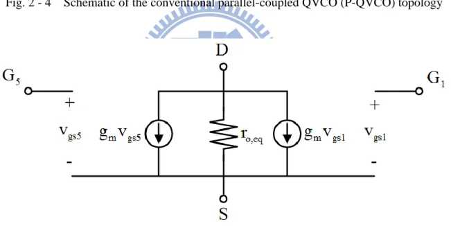
Fig. 2 - 4 Schematic of the conventional parallel-coupled QVCO (P-QVCO) topology
Fig. 2 - 5 Small signal equivalent circuit of the switching- and parallel-coupling transistor
Fig. 2 - 4 shows the conventional parallel QVCO (P-QVCO) where I and Q signals are
generated by coupling two differential VCOs through coupling transistors M5 - M8 in parallel
with switching transistors M1 - M4. Fig. 2 - 5 shows the small signal equivalent circuit of the
switching and corresponding coupling transistors [6]. From Fig. 2 - 5, the coupling strength α
m,couple m5 5
m,switching m1 1
g g W
α= = =
g g W
where gm,couple and gm,switching are the transconductance of coupling transistor and switching
transistor, respectively. In P-QVCO, the coupling strength α has a strong effect on phase noise
and phase error which defines the phase difference from 90。between I and Q signals. For
example, the increase in α degrades the phase noise significantly while the phase error is
reduced, or vice versa. The phase noise degradation is induced by the increase in
transconductance of the coupling transistors. In addition, the increase in α leads to a higher
amount of power dissipation.
Another method to generate quadrature signals has been reported in [17], as shown in
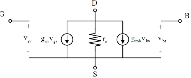
Fig. 2 - 6. In Fig. 2 - 6, the back-gate (body terminal) of the PMOS transistor in one pair of
the VCO is used as the quadrature phase coupling element to the other pair. Consequently the
four quadrature-coupling transistors in the conventional P-QVCO are not needed and their
noise contribution to the oscillator vanishes. As mention above, the P-QVCO has trade-off
between phase noise and phase error. However, in the back-gate-coupling QVCO, phase error
can be reduced without sacrificing phase noise as the coupling involves no additional
transistors. From Fig. 2 - 7, the coupling strength αB through the back-gate can given by
mb m F BS g γ α = = g 2 2Φ -V B
where γ, ΦF, and VBS are the body-effect coefficient, work function, and back-gate (body) to
source bias voltage, respectively. It can be seen that the coupling strength αB is a function of
VBS. Therefore, in order to increase αB, which leads to phase error reduction, the
coupling transistors and therefore additional noise contributions compared to the conventional
coupling transistor based topology.
Fig. 2 - 6 Schematic of the conventional back-gate coupling QVCO
The close-in phase noise spectrum of the circuit shown in Fig. 2 - 6 results from the
flicker noise up-conversion of the NMOS and back-gate modulation PMOS transistor, which
is expressed as [33] 2 2 , , 2 1/ , 1/ , 0 2 2 2 max ( ) 10 log 2 2 n N n Pb f N f Pb i i c f f L q
where c0 is the first Fourier coefficient of the impulse sensitivity function, representation the
wave form symmetry of oscillating signal. The term
2 ,
n N i
f
denotes the summed noise current spectral density from NMOS transistors with angular flicker-noise corner frequency 1/f N, , while 2 , n Pb i f
denotes the one from back-gate modulated PMOS transistors with the angular corner frequency 1/f Pb, . The insertion of the resistor RS at the NMOS source node reduces the transconductance by a factor of 1/(1+gm,NRs), which in turn reduces 1/f N, by the same
factor due to the proportionality of 1/f N, to gm,N for a short-channel MOS transistor [34]. The resistor RS also linearizes the degenerated transconductance variation over an oscillating
swing period. Nevertheless, this method requires an accurate resistor RS which must be
properly designed because large RS may cease the oscillation start-up, introduce extra thermal
noise and introduce an extra amount of power. As mention above, we propose the modified
spontaneous transconductance match (M-STM) technique to conquer this problem.
The circuit we proposed in this chapter can achieve lower phase noise, lower amplitude
imbalance ratio and lower power dissipation by combining the back-gate coupling principle,
current-reused QVCO structure and modified spontaneous transconductance match (M-STM)
2.2
Circuit Design Consideration
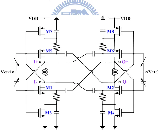
The schematic of the proposed modified spontaneous transconductance match (M-STM)
current reused quadrature VCO (CR-QVCO) is shown in Fig. 2 - 8. The CR-QVCO is mainly
composed of two current reused differential VCO cores, which replaces one of the NMOS
transistors of a conventional differential LC-VCO with a PMOS transistor[11]. The negative
conductances are provided by the cross-connected pairs of transistors M1, M2, and M5, M6,
to compensate the losses in the LC-tank. The series stacking of NMOS transistors and PMOS
transistors allows the supply current to be reduced by half compared to that of the
conventional LC-VCO while providing the same negative conductance.
Fig. 2 - 9 Proposed CR-QVCO operation during each half period
To explain the operation of the proposed CR-QVCO, Fig. 2 - 9 shows the schematic and
corresponding large-signal equivalent circuits during each half period of operation, that is,
when the voltage at node I+ is high and low. As shown in Fig. 2 - 9, during the first
half-period, the transistor M1, M3, M5, and M7 are on and the current flows from VDD to
ground through the inductor. During the second half-period, the transistor, the transistors are
off and the current flows in the opposite direction through the capacitors. Note that in the
conventional differential QVCO, the cross-connected transistors switch alternatively, while in
the proposed QVCO, the PMOS transistors and NMOS transistors switch at the same time.
Unlike a conventional VCO where the transistors switch alternatively, this QVCO does
not have a common-source node because the transistors switch on and off at the same time.
Therefore, the proposed QVCO is inherently immune to phase noise degradation caused by
PMOS-based differential QVCO, the phase noise can be degraded significantly by the noise
near the second harmonic[15]. Utilization of PMOS transistors in the cross-connected pair can
additionally help to reduce the phase noise due to lower flicker noise and hot carrier
effects[16].
Fig. 2 - 10 shows the concept of the proposed modified spontaneous match (M-STM)
technique. During the first half-period, the transistor M3, M4, M7, and M8 are biased in the
triode region as a variable resistor to control the gate-source voltage of M1, M2, M5, and
M6,respectively, which in turn determines the transconductances of M1, M2, M5, and M6. By
connecting the gate terminals to the another side of the outputs, the equivalent resistance of
the variable resistor can be expressed as
ds3 OV3 n ox GS3 t n ox I+ t 3 3 1 1 1 r = = W W V μ C V -V μ C V -V L L
ds4 OV4 n ox GS3 t n ox Q+ t 4 4 1 1 1 r = = W W V μ C V -V μ C V -V L L
ds7 OV7 p ox SG7 t p ox I- t 7 7 1 1 1 r = = W W V μ C V -V μ C VDD-V -V L L
ds8 OV8 p ox SG7 t p ox Q- t 8 8 1 1 1 r = = W W V μ C V -V μ C VDD-V -V L L where μnCox and μpCox are the MOS device parameters, W and L are the gate width and length
of the transistor. The effective transconductances of M1, M2, M5, and M6 in Fig. 2 - 10 can be
expressed, respectively, as
DL m1 n ox OV1 1 n ox I+ t 3 I W g =μ C V -W L μ C V -V L
DR m2 n ox OV2 2 n ox Q+ t 4 I W g =μ C V -W L μ C V -V L
DL m5 p ox OV5 5 p ox I- t 7 I W g =μ C VDD-V -W L μ C VDD-V -V L
DR m6 p ox OV6 6 p ox Q- t 8 I W g =μ C VDD-V -W L μ C VDD-V -V L where μnCox and μpCox are the MOS device parameters, W and L are the gate width and length
and right-half VCO, respectively.
The size of M1 - M8 are selected to satisfy the symmetric oscillation waveform
condition gm1ZI- = gm5ZI+ and gm2ZQ- = gm6ZQ+ where ZI-, ZI+, ZQ-, and ZQ+ denote the
impedance at node I-, I+, Q-, and Q+, respectively. When the output amplitude at node I- and
I+ are different, the feedback mechanism will change the gate voltage of M1 and M5 in an
opposite amount. Therefore, the gm1 and gm5 are complementary changed by feedback
mechanism to equalize the output amplitudes. By the same token, the gm2 and gm6 are also
complementary changed by feedback mechanism to equalize the output amplitudes. The
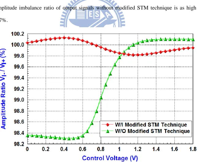
comparison of amplitude ratio V3 / V1 with modified STM technique and without modified
STM technique is shown in Fig. 2 - 11. Over the entire frequency tuning range, the amplitude
imbalance ratio of output signals with modified STM technique is less than 0.2%, while the
amplitude imbalance ratio of output signals without modified STM technique is as high as
1.7%.
Fig. 2 - 11 Simulated output amplitude imbalance ratio of the proposed modified STM-QVCO
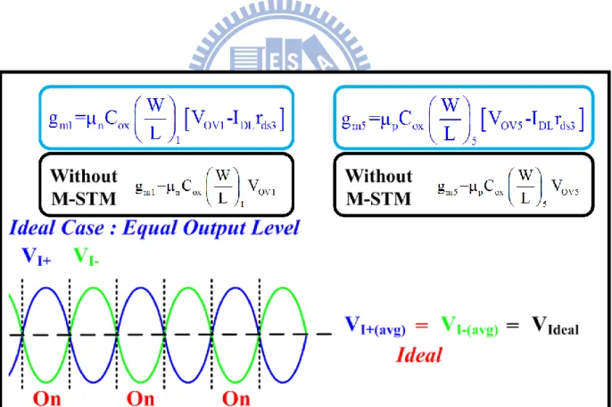
The mechanism of the proposed modified spontaneous transconductance match (M-STM)
technique can be divided into five state, as shown from Fig. 2 - 12 to Fig. 2 - 16 :
I. Ideal Case - Equal Output Level : VI+(avg) = VI-(avg) = VIdeal
As shown in Fig. 2 - 12, when the gmn and gmp has been properly designed, two
outputs of the CR-QVCO will exhibit perfectly equal output level, i.e., VI+(avg) = VI-(avg).
We give this ideal value a name VIdeal and will be used later.
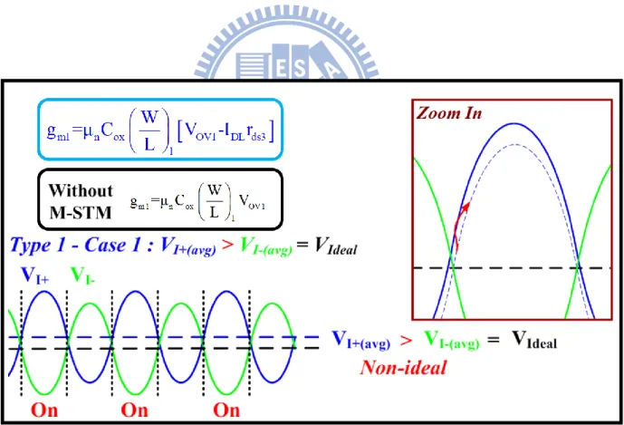
II. Type 1 - Case 1 : VI+(avg) > VI-(avg) = VIdeal
As shown in Fig. 2 - 13, when the NMOS process transconductance coefficient “kn” has slightly become smaller due to process variation :
1. VI+(avg) will become larger than ideal value correspondingly.
2. The larger VI+(avg) will lead to smaller rds3, and , in turn, increase VI+(avg) toward
the ideal value, which is the dashed line in the zoom in window.
Consequently, VI+(avg) will have less variation thanks to the M-STM feedback
compensation.
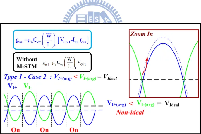
III. Type 1 - Case 2 : VI+(avg) < VI-(avg) = VIdeal
As shown in Fig. 2 - 14, when the NMOS process transconductance coefficient “kn” has slightly become larger due to process variation :
1. VI+(avg) will become smaller than ideal value correspondingly.
2. The smaller VI+(avg) will lead to larger rds3, and , in turn, increase VI+(avg) toward
the ideal value.
Consequently, VI+(avg) will have less variation thanks to the M-STM feedback
compensation.
IV. Type 2 - Case 1 : VI-(avg) > VI+(avg) = VIdeal
As shown in Fig. 2 - 15, when the PMOS process transconductance coefficient “kp” has slightly become smaller due to process variation :
1. VI-(avg) will become smaller (but larger negative-half amplitude) than ideal
value correspondingly.
2. The smaller VI-(avg) will lead to smaller rds7, and , in turn, increase VI-(avg)
toward the ideal value.
Consequently, VI-(avg) will have less variation thanks to the M-STM feedback
compensation.
V. Type 2 - Case 2 : VI-(avg) < VI+(avg) = VIdeal
As shown in Fig. 2 - 16, when the PMOS process transconductance coefficient “kp” has slightly become larger due to process variation :
1. VI-(avg) will become larger (but smaller negative-half amplitude) than ideal
value correspondingly.
2. The larger VI-(avg) will lead to larger rds7, and , in turn, decrease VI-(avg) toward
the ideal value.
Consequently, VI-(avg) will have less variation thanks to the M-STM feedback
compensation.
2.3
Chip Layout and Simulation Results
The circuit was simulated and optimized using Agilent ADS. The design procedure can
be divided in two steps. First, a small signal analysis was used to optimize the feedback and
the resonator elements to find the oscillation condition at the target frequency. This condition
was simulated breaking the feedback path. In the second step, a large signal analysis was
performed with the harmonic balance simulator to predict the exact oscillation frequency and
output power of the fundamental signal as well as the harmonic signals.
Fig. 2 - 17 shows the chip layout photograph of the proposed modified STM current
reused QVCO, which is designed and implemented in TSMC 0.18μm mixed-signal/RF
CMOS 1P6M technology. The chip size is 1.100 × 0.841 mm2 including all pads and bypass
capacitances. Each buffer of the QVCO outputs were designed as a common-source amplifier.
Fig. 2 - 18 Simulated phase noise of the proposed modified STM-QVCO
The simulated phase noise and tuning range of the proposed modified STM QVCO are
shown in Fig. 2 - 18 and Fig. 2 - 19,respectively. Table 2 - 1 summarizes the simulated results
of the proposed modified STM QVCO in each corner. The figure of merits (FOM) for
oscillators summarizes the important performance parameters, i.e., phase noise and power
consumption P, to make a fair comparison is defined in [40] as
20 log 10 log( ) 1 O P FOM L mW where the second term is to neutralize the effect of offset in L(Δω) while taking the center
frequency into account. The power consumption is calculated as dBm such that the unit of
FOM remains the same as that of L(Δω).
Table 2 - 1 Simulated results of the proposed modified STM-QVCO
Corner SS TT FF SF FS Tuning Range 4.78-5.12 4.82-5.13 4.91-5.22 4.84-5.16 4.86-5.16 Phase Noise -118.645 -118.322 -118.102 -118.571 -118.313 Supply Voltage 1.5 1.35 1.2 1.35 1.35 ID 3.6 3.41 3.53 3.49 3.38 Core Power 4.68 4.60 4.24 4.71 4.56 FOM -185.53 -185.35 -185.64 -185.53 -184.90
2.4
Measurement Results and Discussion
2.4.1 Measurement Consideration
The proposed QVCO are designed for on-wafer testing, and the DC voltage are supplied
by two sets of six-pin probe, so that the distance between each DC pad must more than 50μm
to satisfy the probe testing rules. The output buffer of each quadrature output is designed
using common-source amplifier, and the drain end of each buffer is connected to the RF pad.
For measurement, we connect four bias-tee terminals to the corresponding RF pads as shown
in Fig. 2 - 20.
Fig. 2 - 20 Bias-Tee Model
The phase noise, tuning range, output spectrum and output waveform are measured using
signal source analyzer (Agilent E5052B) and digital signal analyzer (Agilent DSA91204A)
Fig. 2 - 21 Signal Source Analyzer (Agilent E5052B)
Fig. 2 - 23 Chip photo of the proposed modified STM-QVCO
The Chip photo of the proposed modified STM-QVCO is shown in Fig. 2 - 23. Fig. 2 - 24
and Fig. 2 - 25 shows the arrangement of DC and RF probes. The measured phase noise at
4.84GHz, output spectrum, tuning range, output waveform, and amplitude imbalance ratio
was shown in Fig. 2 - 26 to Fig. 2 - 30, respectively. Table 2 - 2 summarizes the measured
Fig. 2 - 24 Arrangement of DC and RF probes
Fig. 2 - 26 Measured phase noise of the proposed modified STM-QVCO
Fig. 2 - 30 Measured output amplitude imbalance ratio of the proposed modified STM-QVCO
Table 2 - 2 Comparison of QVCO Performance Technolog y Tuning Range Phase Noise Supply Voltage Core Power FOM This work (Chapter 2) 0.18μm CMOS 4.84-5.17 GHz -117.4 dBc/Hz@ 1MHz 1.3V 5.04mW -184.07 This work (Chapter 3) 0.18μm CMOS 4.83-5.30 GHz -125.8 dBc/Hz@ 1MHz 1.3V 3.64mW -193.87 [7] MWCL, 2009 0.18μm CMOS 4.39-5.26 GHz -113.65 dBc/Hz@ 1MHz 1.8V 6.3mW -180.0 [8] MWCL, 2005 0.18μm CMOS 5.50-6.10 GHz -115 dBc/Hz@ 1MHz 1.8V 1.84mW -182.2 [42] MWCL, 2009 0.18μm CMOS 2.05-2.47 GHz -117 dBc/Hz@ 1MHz 1.8V 2.84mW -184 [43] MWCL, 2009 0.18μm CMOS 4.38-4.71 GHz -120.8 dBc/Hz@ 1MHz 1.1V 2.55mW -189.61 [9] MWCL, 2007 0.18μm CMOS 1.83-2.02 GHz -124 dBc/Hz@ 1MHz 1.25V 2.2mW -186.7 [17] MWCL, 2009 0.18μm CMOS 3.01-3.49 GHz -133 dBc/Hz@ 1MHz 1.5V 8.1mW -193.5
Chapter 3
Current-Reused Low Phase Noise Quadrature VCO
with Self-Switching Bias
3.1
Introduction
Quadrature signals finds application in many communication systems. For high speed
clock and data recovery systems, quadrature signals are required for frequency detection,
half-rate phase noise detection, and phase interpolation [19] - [21]. For RF front-ends,
quadrature signals are necessary in the implementation of image rejection and direct
conversion transceivers, where they are used for modulation or demodulation requirements.
As we mentioned in chapter 2, there are several methods to generate quadrature signal.
In fact, a widely-used approach for generation the quadrature signals at high operation
frequencies is to cross couple two identical LC oscillator so as to take advantage of the
superior performance achievable with LC resonators. In this case two oscillators can be
connected in such a way that a signal from one oscillator is injected into the second oscillator
and a signal from the second oscillator is injected into the first. The result is that the two
oscillators become locked in frequency with quadrature outputs. LC-VCOs have good phase
noise performance due to their inherent frequency selectivity that can suppress side-band
noise.
Fig. 3 - 1 shows the well-known implementation of Quadrature negative Gm Oscillator
coupling transistor (M5-M8) in parallel with the core negative-resistance transistor (M1-M4).
This technique, however, suffers from the trade-off between phase noise and accuracy. The
coupling transistors connected in parallel further degrades the phase noise and the power
consumption significantly. To improve the performance, the coupling transistor (M5-M8) can
be connected in series with the negative-resistance transistors (M1-M4), such that the phase
noise contribution from the coupling device can be reduced as a result of degeneration in
cascode configuration. The trade-off between phase noise and phase accuracy can be relaxed.
Fig. 3 - 1 Schematic of the conventional parallel-coupled QVCO (P-QVCO)
As shown in Fig. 3 - 2, one of the methods of series coupling is referred as the Top-Series
(TS) QVCO [22], [23]. Since the coupling transistor does not require an additional biasing
current, power consumption is reduced in this topology. The phase error is almost independent
of coupling strength αB . In fact, phase error of the TS-QVCO acts like a design constant
dependent on the actual amount of mismatch between ideally identical components. When
both TS-QVCO and P-QVCO are designed to have the same coupling strength, center
Fig. 3 - 2 Schematic of the conventional top series-coupled QVCO (TS-QVCO)
The major problem with this architecture is that the coupling transistors have to be about five
times larger than the negative resistance transistors [24], thus loading the oscillator with large
parasitic capacitances that reduce the tuning range, making this solution unsuitable for high
frequency and wideband application.
There is an alternative way to achieve series coupling, as shown in Fig. 3 - 3, known as
the Bottom Series (BS) QVCO [25]. In this configuration the coupling transistor is placed at
the bottom of the switching transistor. As for the TS-QVCO, the phase error is almost
independent of coupling strength αB. When both BS-QVCO and P-QVCO display the same
phase-error and have the same center frequency and power consumption, BS-QVCO has a
higher figure of merit (FOM). However, to compare with TS-QVCO, BS-QVCO has a higher
FOM but also a higher phase error than TS-QVCO.
![Fig. 1 - 7 A typical phase noise plot for a free running oscillator, [33]](https://thumb-ap.123doks.com/thumbv2/9libinfo/8508681.185703/20.892.143.794.148.1051/fig-typical-phase-noise-plot-free-running-oscillator.webp)
![Fig. 1 - 10 Conversion of a low frequency sinusoidal current to phase, [33]](https://thumb-ap.123doks.com/thumbv2/9libinfo/8508681.185703/24.892.135.797.139.1075/fig-conversion-low-frequency-sinusoidal-current-phase.webp)