Resistive switching characteristics of ytterbium oxide thin
film for nonvolatile
memory application
Hsueh-Chih Tseng
a, Ting-Chang Chang
a,b,⁎
, Jheng-Jie Huang
a, Yu-Ting Chen
c, Po-Chun Yang
c,
Hui-Chun Huang
d, Der-Shin Gan
d, New-Jin Ho
d, Simon M. Sze
e, Ming-Jinn Tsai
fa
Department of Physics, National Sun Yat-Sen University, Kaohsiung, 804, Taiwan, ROC
b
Center for Nanoscience & Nanotechnology, National Sun Yat-Sen University, Kaohsiung, 804, Taiwan, ROC
c
Department of Electro-Optical Engineering, National Sun Yat-Sen University, Kaohsiung, 804, Taiwan, ROC
d
Department of Materials Science and Engineering, National Sun Yat-Sen University, Kaohsiung, 804, Taiwan, ROC
eInstitute of Electronics, National Chiao Tung University, Hsin-Chu, 300, Taiwan, ROC f
Electronics and Opto-electronics Research Laboratories, Industrial Technology Research Institute, Hsinchu, Taiwan, ROC
a b s t r a c t
a r t i c l e i n f o
Available online 23 July 2011 Keywords:
Nonvolatile resistance switching memory RRAM
Yb2O3
Forming
This paper studies the effects of both the positive and negative forming processes on the resistive switching characteristics of a Pt/Yb2O3/TiN RRAM device. The polarity of the forming process can determine the transition mechanism, either bipolar or unipolar. Bipolar behavior exists after the positive forming process, while unipolar behavior exists after the negative forming process. Furthermore, the bipolar switching characteristics of the Pt/Yb2O3/TiN device can be affected by using a reverse polarity forming treatment, which not only reduces the set and reset voltage, but also improves the on/off ratio.
Crown Copyright © 2011 Published by Elsevier B.V. All rights reserved.
1. Introduction
Resistive random access memory (RRAM) has attracted considerable interest for the next generation of nonvolatile memory devices due to its simple structure, low operation voltage and process compatibility with
the present CMOS industry[1]. Many materials have been demonstrated
to achieve resistive switching characteristics, such as perovskite oxides
Pr0.7Ca0.3MnO3and SrZrO3[2,3]and binary metal oxides such as Al2O3,
ZrO2, MnO2, CuO, NiO and TiO2 [4–9]. Two dominant resistance
switching mechanisms have been proposed. One is oxygen vacancy
nucleation at a metal/oxide interface[10,11]. The other mechanism is
the conductivefilament model, which describes the formation/rupture
of a metallicfilament using a metal such as Cu or Ag acting as mobile ions
in the oxide[12]. Recently, rare earth (RE) metal oxides, which are used
as a high-k gate insulator for advanced complementary
metal-oxide-semiconductor (CMOS) technology[13,14], have been demonstrated to
exhibit resistance switching phenomena[15,16]. One of the RE metal
oxides, ytterbium oxide (Yb2O3), is attractive as a gate dielectric in CMOS devices because of its dielectric constant of 15, larger energy band
gap (N5 eV), and predicted chemical and thermal stability with Si.
Therefore, it also has been explored for semiconductor applications including memory devices, logical devices and optoelectronic devices
[17]. Up to now, the application of Yb2O3 in the resistive switchingfield
has not been researched.
This work investigates resistance switching characteristics in a Pt//
Yb2O3/TiN structure by using both the positive forming (PF) and
negative forming (NF) processes. In addition, after the PF process, a reverse polarity forming (RPF) treatment is also studied. A mechanism is
proposed to explain the influence on resistive switching characteristics
of the Yb2O3-based RRAM of the device after a PF process both with and
without an additional RPF treatment.
2. Experiment
Yb2O3 thin film of 20 nm thickness was deposited on a TiN/Si
substrate by reactive magnetron RF sputtering an Yb2O3target in Ar
(30 sccm) ambient at room temperature. The RF sputtering power and pressure of the sputter system were set to 150 W and 4 mTorr. Next, the Pt top electrode (TE) was deposited and patterned by the liftoff process. High-resolution transmission electron microscopy (HRTEM)
was used to observe lattice images of the Yb2O3thinfilm, and X-ray
photoelectron spectroscopy (XPS) was employed to determine the
chemical bonding state of the Yb2O3thinfilms. The standard sample
was PF treated, whereas the control sample used as reference was a standard sample with additional RPF treatment, and will be referred to as standard and control samples hereafter. Additionally, another sample activated by the NF process was used to clarify the effects of the RPF treatment. The temperature dependence of resistance in the low resistance state (LRS) of these three samples was observed. All
electrical characteristics were measured over an 8μm×8 μm cell size
with an Agilent B1500 semiconductor parameter analyzer. During
Thin Solid Films 520 (2011) 1656–1659
⁎ Corresponding author at: Department of Physics, National Sun Yat-Sen University, 70 Lien-Hai Road, Kaosiung, Taiwan 80424, ROC. Tel.: + 886 7 5252000 3708; fax: + 886 7 5253709.
E-mail address:[email protected](T.-C. Chang).
0040-6090/$– see front matter. Crown Copyright © 2011 Published by Elsevier B.V. All rights reserved. doi:10.1016/j.tsf.2011.07.026
Contents lists available atScienceDirect
Thin Solid Films
these measurements, bias was applied to the TiN bottom electrode (BE) while the Pt top electrode (TE) was grounded.
3. Results and discussion
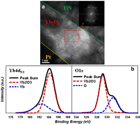
In order to ascertain the switching mechanism, HRTEM was performed to analyze this structure. Many studies have indicated that the grain boundary can induce multiple conductive paths. As shown in
Fig. 1(a), many grain boundaries are observed in the as-deposited
Yb2O3thinfilm. Therefore, multiple conductive paths can be formed,
such as Yb or semiconducting YbOx.Fig. 1(b) shows the XPS analysis
which investigates the chemical states of ytterbium and oxygen. The
Yb 4d5/2spectrum indicates a coexistence of Yb+ 3and metallic Yb in
Yb2O3, with Yb+ 3(Yb+ 3at 184.1 eV) making up the majority and
metallic Yb (Yb0+ at 182 eV) the minority. Furthermore, the O1s
spectrum indicates a similar coexistence of lattice oxygen ions, with a
majority of O−2(O−2at 529.1 eV) and a smaller amount of nonlattice
oxygen ions (O0+at 531 V). Kang et al.[18]ascribes the forming free
behavior in ZnO-based devices to the abundant oxygen vacancies and
the pre-existing nonlattice oxygen ions in the ZnOfilms. These results
imply that the forming process is mandatory for this device before use as a memory device.
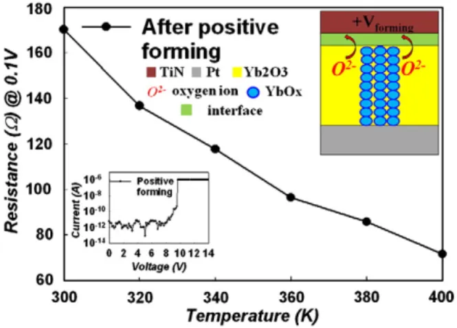
As mentioned above, the forming process is necessary to activate
the RRAM device. During the PF process, as shown in the inset ofFig. 2,
a positive DC bias of about 14 V was applied to the BE with a current
compliance of 1μA. Then, many conductive paths occurred as a result
of dielectric breakdown, with the resistance state (RS) then
transforming from initial high resistance state (HRSinitial) to initial
LRS (LRSinitial). This can be attributed to a dynamic process of breaking
the chemical bonds to generate oxygen vacancies and nonlattice oxygen ions. Hence, the nonlattice oxygen ions can drift towards the
anode and form TiOxat the TiN/oxide interface due to the electrical
field[19,20], resulting in many defects or oxygen vacancies along the
leakage paths[21], as shown in the inset schematic diagram ofFig. 2.
In addition,Fig. 2shows the temperature dependence of resistance
after activating the device, where the LRSinitialdecreases when the
ambient temperature increases, as is typical of semiconductor
behavior[22]. Because of the interface formation, the voltage across
the device can be divided between the bulk and interface region, which prevents the bulk region from continually generating more oxygen ions. From this result, it can be inferred that the conductive paths consist of semiconducting oxide or oxygen vacancies.
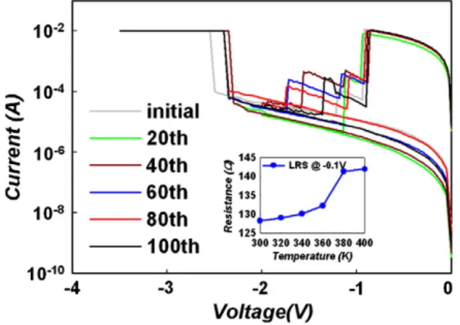
Fig. 3shows the typical bipolar switching behavior of the Pt/Yb2O3/
TiN device. The transition between LRS and HRS is observed for 100 cycles by using dc voltage sweeping mode. First, during the set process, a predetermined sweeping voltage of about 2 V with 10 mA current compliance was applied, after which there is a sudden increase
in current observed at about 1.5 V, which is defined as Vset. In a
subsequent sweep, the LRS was achieved during backward sweeping from 2 V to 0 V. In a similar fashion during the reset process, the RS can
be restored to HRS by using a negative sweeping voltage of about−2 V,
with the current starting to decrease at about−1.4 V, which is defined
as Vreset. In a subsequent sweep, the HRS was achieved during the
backward sweeping from−2 V to 0 V. Recent studies have indicated
that the bipolar resistance switching is related to the redox reaction near
the anode-electrode/oxide interface[19], as shown in the inset ofFig. 3.
However, during RPF treatment, as shown in the inset ofFig. 4, a
higher and reverse polarity dc bias with a 10 mA current compliance was applied to the standard device. The anode-electrode interface layer decomposed and the adjacent conductive path(s) rupture and
reform, as shown in the inset schematic diagram ofFig. 4. First, when
the bias increases to about−3 V, there is a noticeable transformation
in RS, which suddenly transforms from LRS to the new HRSinitial. This
violent RS transformation of RPF reveals that the multiple and redundant conducting paths are eliminated by the Joule Heating effect
[23]. Some research has indicated that the reset behavior is due to the
annihilation of oxygen vacancies or oxidation of the conductive paths
[20,21,24]. Subsequently, when the bias continues to increase, at
about−5 V the RS transforms again from the new HRSinitialto new
LRSinitial, which is similar to the forming process. Then, the oxygen
Fig. 1. (a) High-resolution transmission electron microscopy (HRTEM) image. (b) XPS spectra of Yb 4 d5/2 and O 1 s.
1657 H.-C. Tseng et al. / Thin Solid Films 520 (2011) 1656–1659
vacancies and oxygen ions can be generated again; moreover, these oxygen ions drift to Pt and can be chemisorbed at the grain boundary
or penetrate through the Pt layer [21,24]. Fig. 4 shows that the
temperature dependence of resistance in the new LRSinitialincreases
when the ambient temperature increases. The interface of TiN has decomposed; indeed, Pt cannot be thoroughly oxidized. The cross voltage can act completely on the bulk region, so there is a metallic
behavior of the conductive paths[22]. Furthermore, a few cycles of
unipolar switching phenomena appear momentarily after the RPF treatment.
The transition between the LRS and HRS of the control sample was observed for 100 cycles by using the same dc voltage sweeping mode
as the standard sample, as shown in Fig. 5. Compared with the
standard samples, the Vsetand Vresetof the control samples are lower.
The inset ofFig. 5shows that, after the bipolar switching mode, the
temperature dependence of resistance, including LRS and HRS, decreases when ambient temperature increases, again typical of
semiconducting behavior[22]. The oxygen ions drift towards TiN and
reconstruct the interface layer during the set process. Thus, a different transition of RS induces change from metallic behavior to semicon-ducting behavior because the TiN interface is still the redox reaction region. The force required to break the chemical bonds of the set process is weaker than the forming process, resulting in a thinner interface layer.
The negative differential (NDF) region of on current, which is located in the negative bias region, affects the growth rate of HRS.
Fig. 5indicates that the lower Vresetinduces the longer NDF region,
and the larger HRS of the control sample can be achieved by applying
the same stopping voltage, as shown inFig. 6. In addition, because
many studies have indicated that reconstruction of the conductive
path(s) occurs in only a single path [25], this larger HRS can be
attributed to a decrease of conductive paths. Thus, the redox reaction is more concentrated at residual conductive paths, as shown in the
inset ofFig. 6. Generally speaking, the set process is a soft breakdown
phenomenon, and is related to metal/oxide interfacial quality and thickness. For this reason, the thinner interface layer can not only
cause a reduced Vset, but can also cause lower LRS.
The RPF treatment in Yb2O3thinfilm causes the decomposition of
the anode-electrode interface layer and the rupture/reformation of the conductive path(s). For comparison with the RPF treatment device, the negative forming (NF) process device is shown in the inset ofFig. 7. The RS changes from HRSinitialto LRSinitialby applying a
negative voltage of about−14 V to the BE. According to this polarity,
the oxygen ions migrate towards TE. Many studies have indicated that
the oxidation of Pt is difficult to achieve[20,21,24]. Hence, as shown in
the inset schematic diagram ofFig. 2, the conductive paths may
consist of Yb metal atoms, such as the NiO-based system[25,26].
Additionally, Fig. 7 shows that this LRSinitialincreases as ambient
temperature rises, which is similar to typical metallic behavior. A
comparison of the temperature dependence of LRSinitialfor PF and NF
shows opposite tendencies.
Finally, after the NF process, the RS switching behaviors have a
clear transformation from a bipolar to a unipolar mechanism.Fig. 8
shows the typical unipolar switching behaviors of the Pt/Yb2O3/TiN
Fig. 2. Temperature dependence resistance in LRSinitialfor the standard sample, with a
0.1 V reading voltage. The inset shows the positive forming I–V curve and schematic diagram of the measurement system.
Fig. 3. Typical bipolar resistive switching I–V curves for the standard sample. The inset shows a schematic diagram of the switching mechanism.
Fig. 4. Temperature dependence resistance in LRSinitialfor the control sample, with a−0.1 V
reading voltage. The inset shows the RPF treatment I–V curve and the schematic diagram of the measurement system.
Fig. 5. Typical bipolar resistive switching I–V curves for the control sample. The inset shows temperature dependence resistance in LRS and HRS.
device. The transition between LRS and HRS was observed for 100 cycles by using dc voltage sweeping mode. First, starting at 0 V
and sweeping to−3.5 V with a 10 mA current compliance, a sudden
increase of leakage current is observed at a voltage of about−2.3 V,
defined as the Vuni-set, with the RS able to be stored in LRS. Then,
starting again at 0 V and sweeping to−2 V a sudden drop of current
around−1 V was observed, defined as Vuni-reset, with a restoration of
the RS to the HRS. Therefore, as shown in the inset ofFig. 8, the
temperature dependence of LRS indicates that the resistance increases as ambient temperature rises. This temperature dependence phe-nomenon in the conductive path is similar to RPF treatment, which is typically metallic in behavior.
4. Conclusion
In conclusion, the effect of a PF and a NF on resistive switching
characteristics of a Pt/Yb2O3/TiN RRAM device has been investigated.
Results indicate that the switching mechanism is dependent on the polarity of the forming process, and also affects the metal/oxide interface layer decomposition and formation. Therefore, applying the reverse polarity forming treatment for the standard sample which has been activated by the PF process can obtain better bipolar switching characteristics such as lower set and reset voltages, and a larger on/off ratio. This work demonstrates the improvement of switching characteristics by using the reverse polarity forming treatment.
Acknowledgment
This work was performed at National Science Council Core Facilities Laboratory for Nano-Science and Nano-Technology in Kaohsiung-Pingtung area and was supported by the National Science Council of the Republic of China under contract nos. NSC-99-2120-M-110-001 and NSC-97-2112-M-110-009-MY3.
References
[1] K. Szot, W. Speier, G. Bihlmayer, R. Waser, Nat. Mater. 5 (4) (2006) 312. [2] A. Sawa, T. Fujii, M. Kawasaki, Y. Tokura, Appl. Phys. Lett. 85 (2004) 4073. [3] C.Y. Liu, P.H. Wu, A. Wang, W.Y. Jang, J.C. Young, K.Y. Chiu, T.Y. Tseng, IEEE Electron
Device Lett. 26 (6) (2005) 351.
[4] C.Y. Lin, C.Y. Wu, C.Y. Wu, C. Hu, T.Y. Tseng, J. Electrochem. Soc. 154 (9) (2007) G189. [5] C.Y. Lin, C.Y. Wu, C.Y. Wu, T.C. Lee, F.L. Yang, C. Hu, T.Y. Tseng, IEEE Electron Device
Lett. 28 (5) (2007) 366.
[6] M.K.Y.J.W. Park, T.K. Ko, L.K. Lee, Appl. Phys. Lett. 95 (2009) 042105.
[7] R. Dong, D.S. Lee, W.F. Xiang, S.J. Oh, D.J. Seong, S.H. Heo, H.J. Choi, M.J. Kwon, S.N. Seo, M.B. Pyun, M. Hasan, H. Hwang, Appl. Phys. Lett. 90 (2007) 42107. [8] G.S. Park, X.S. Li, D.C. Kim, R.J. Jung, M.J. Lee, S. Seo, Appl. Phys. Lett. 92 (2007)
222103.
[9] B.J. Choi, D.S. Jeong, S.K. Kim, C. Rohde, S. Choi, J.H. Oh, H.J. Kim, C.S. Hwang, K. Szot, R. Waser, B. Reichenberg, S. Tiedke, J. of Phys. Lett. 98 (2005) 33715. [10] J.J. Yang, F. Miao, M.D. Pickett, D.A.A. Ohlberg, D.R. Stewart, C.N. Lau, R.S. Williams,
Nanotechnology 20 (2009) 215201.
[11] C. Yoshida, K. Kinoshita, T. Yamasaki, Y. Sugiyama, Appl. Phys. Lett. 93 (2008) 042106.
[12] C. Schindler, G. Staikov, R. Waser, Appl. Phys. Lett. 94 (2009) 072109. [13] A. Fissel, M. Czernohorsky, H.J. Osten, Superlattices Microstruct. 40 (2006) 551. [14] L. Marsella, V. Fiorentini, Phys. Rev. B 69 (2004) 172103.
[15] X. Cao, X. Li, X. Gao, W. Yu, X. Liu, Y. Zhang, L. Chen, X. Cheng, J. Phys. Lett. 106 (2009) 073723.
[16] K.C. Liu, W.H. Tzeng, K.M. Chang, Y.C. Chan, C.C. Kuo, C.W. Cheng, Microelectron. Reliab. 50 (2010) 670.
[17] T.M. Pan, W.S. Huang, Appl. Surf. Sci. 255 (2009) 4979.
[18] N. Xu, L. Liu, X. Sun, X. Liu, D. Han, Y. Wang, R. Han, J. Kang, B. Yu, Appl. Phys. Lett. 92 (2008) 232112.
[19] S.Y. Wang, D.Y. Lee, T.Y. Tseng, C.Y. Lin, Appl. Phys. Lett. 95 (2009) 112904. [20] S. Yu, H.-S. Philip Wong, IEEE Electron Device Lett. 31 (12) (2010) 1455. [21] L. Goux, P. Czarnecki, Y.Y. Chen, L. Pantisano, X.P. Wang, R. Degraeve, B.
Govoreanu, M. Jurczak, D.J. Wouters, L. Altimime, Appl. Phys. Lett. 97 (2010) 243509.
[22] C. Chen, Y.C. Yang, F. Zeng, F. Pan, Appl. Phys. Lett. 97 (2010) 083502. [23] S.H. Chang, J.S. Lee, S.C. Chae, S.B. Lee, C. Liu, B. Kahng, D.-W. Kim, T.W. Noh, Phys.
Rev. Lett. 102 (2009) 026801.
[24] L. Goux, z.X.P. Wang, Y.Y. Chen, L. Pantisano, N. Jossart, B. Govoreanu, J.A. Kittl*, M. Jurczak, L. Altimime, D.J. Wouters, Electrochem. Solid-State Lett. 14 (6) (2011) H244.
[25] U. Russo, D. Ielmini, C. Cagli, A.L. Lacaita, IEEE Trans. Electron Devices 56 (2) (2009) 193.
[26] H. Shima, F. Takano, H. Akinaga, Tamai Yukio, I.H. Inoue, H. Takagi, Appl. Phys. Lett. 91 (2007) 012901.
Fig. 6. LRS and HRS statistics for standard and control samples for 100 cycles in dc sweeping mode, with a 0.1 V reading voltage. The inset shows a schematic diagram of the switching mechanism.
Fig. 7. Temperature dependence resistance in LRSinitialfor the sample activated by
negative forming process, with a−0.1 V reading voltage. The inset shows the negative forming I–V curve and the schematic diagram of the measurement system.
Fig. 8. Typical unipolar resistive switching I–V curves for the sample activated by negative forming process. The inset shows temperature dependence resistance in LRS, with a−0.1 V reading voltage.
1659 H.-C. Tseng et al. / Thin Solid Films 520 (2011) 1656–1659