國 立 交 通 大 學
電 機 與 控 制 工 程 學 系
碩 士 論 文
以FPGA實現VRM多相交錯式數位控制器
Design and Implementation of an FPGA-Based Digital
Multiphase-Interleaved VRM Controller
研 究 生:王翊仲
指導教授:鄒應嶼 博士
以 FPGA實 現 VRM多 相 交 錯 式 數 位 控 制 器
研究生:王翊仲 指導教授:鄒應嶼 博士
國立交通大學電機與控制工程學研究所 中文摘要
本文提出以單晶片場可規劃邏輯陣列(field programmable gateway array, FPGA) 來實現電壓調節模組(voltage regulator modules, VRM)的多相交錯式數位控器,包含 交錯式電流取樣以及負載電流前饋補償。在降壓轉換器中,開關切換時電感電流 的取樣訊號將會與脈寬調變(pulse width modulation, PWM)訊號同步。文中提出的 取樣方法能有效避免開關切換所造成的雜訊,在取樣週期中,電流將會正確地被 感測。藉由數位的介面將微處理器與負載做連結,用前饋補償的方式依照時脈、 負載、以及運算時間來做輸出電壓的調整。數位控制器以及脈寬調變產生器的時 脈在同一個取樣頻率下延遲,而達到互相交錯的效果。整個 VRM 的數位控制架構 將會在文中被提及,同時針對微處理器快速動態響應的部份做模擬分析以及電路 實驗驗證。 關鍵詞:數位 VRM 控制器,單晶片 FPGA 實現,交錯式取樣控制架構,同步電流取 樣技術
Design and Implementation of an FPGA-Based Digital
Multiphase-Interleaved VRM Controller
Student: Yi-Chung Wang Advisor: Dr. Ying-Yu Tzou
Department of Electrical and Control Engineering National Chiao Tung University
Abstract
This thesis presents the design and implementation of a singe-chip FPGA based digital VRM controller for multi-phase synchronous buck converters with interlaced current sampling and load current feed-forward compensation techniques. The sampling of the inductor current is synchronized with the PWM signal in synchronous buck converter for both turn-on and turn-off. The proposed sampling scheme has immunity to the switching noise. A true average current signal with minimum response time can be measured with accuracy within a switching period. The timing clocks for the digital controller and the digital PWM generator are interleaved with each other to achieve a minimum delay at a same sampling and switching frequency. A digital interface is designed for the connected microprocessor load to adjust the output voltage and provide feed-forward load current compensation according to its clock rate, loading factor, and pipeline scheduling. The realization scheme for the proposed digital VRM controller has been described. Simulation analysis and experimental verifications are given to illustrate the fast dynamic response control of VRM for advanced microprocessors.
Keywords : digital VRM controller, single-chip FPGA implementation, interleaved sampling and control scheme, synchronous current sampling technique
誌 謝
首先特別感謝我的老師鄒應嶼教授這兩年多來的指導。老師讓我理解了研 究生主要的本質是在解決問題,而並不是單純的汲取知識,這點對我影響甚鉅。 對問題和結果同樣看重的指導理念,也令我在思索發問的過程中有所得。這兩年 來對於研究的方法以及觀念之能夠有所進步,實在相當感謝老師。 感謝博班育宗學長,常常解決我在研究上的困惑,並在思考問題以及論文 寫做上面給予幫助。也感謝啟揚、哲韋、建強三位碩班的學長,無論是在生活或 是研究上,總是把自己所知無私地分享。 從大學部同窗至今六年的好友晏銓、韋吉、少軍、智達,這兩年的生活因 為你們而格外顯得有意義,我想我永遠不會忘記這段共同熬夜拼截稿、成群去覓 食、以及一同出遊的日子。謝謝學弟哲維、宗磬,讓實驗室氣氛活絡了起來,使 我的研究生活更多彩多姿。謝謝助理月貴的關照,幫忙處理實驗室的事情。 我很慶幸能進入本實驗室這個大家庭,和大家一起奮鬥。我會永遠珍惜這 段日子,這份同甘共苦革命般的情感。 最後,我要特別感謝父母與家人,雖然我的研究生涯中回花蓮的日子並不 長。他們總是在我低潮時支持我並給我鼓勵。我相當高興能將將此榮耀和喜悅與 他們一起分享。 王翊仲 2007 仲夏 新竹TABLE OF CONTENTS
Abstract (Chinese) ...i
Abstract (English) ... ii
Table of Contents...iv
List of Tables ...vi
List of Figures... vii
Chapter 1 Introduction ...1
1.1 Research Background and Recent Development ...1
1.2 Research Motivation and Objectives ...3
1.3 Research Method and System Description ...4
1.4 Thesis Organizations...6
Chapter 2 Review and Analysis of VRM ...7
2.1 Mathematical Modeling of Voltage Regulator Module...7
2.2 Basic Operational Principles for Voltage Regulator Module ...9
2.2.1 Inductor Current Ripple ...10
2.2.2 Output Voltage Ripple ...11
2.2.3 Load Changing Issue...12
Chapter 3 Digital VRM Controller Design...13
3.1 Digital Control Structure...13
3.2 Current Loop Control...15
3.2.1 Current Loop Analysis ...15
3.2.2 Current Loop Controller Design ...16
3.3 Voltage Loop Control ...18
3.3.1 Voltage Loop Analysis...18
3.3.2 Voltage Loop Controller Design...19
3.4 Pulse Width Modulation Control ...19
Chapter 4 Implementation and Setup of the Digital VRM Controller...22
4.2 Implementation of Digital Compensator ...23
4.2.1 Fixed-point Computation ...23
4.2.2 Implementation of Proportional-Integral Controller...24
4.2.3 Implementation of Phase Lead Controller ...30
4.3 Implementation of Digital Pulse Width Modulation Generator ...32
4.3.1 Implementation of Carrier Generator...34
4.3.2 Implementation of Phase Shifter...35
4.3.3 Implementation of Dead-Time Generator...36
4.4 Implementation of Synchronous Sampling Signal Generator ...37
Chapter 5 Experimental Verification and Simulation Result ...42
5.1 Verification of Block for Digital Control ...42
5.2 Simulation Result...45
Chapter 6 Conclusion ...51
References...52
LIST OF TABLES
3.1 Converter Design Parameters. ... 14
4.1 Pin Definition of the Deadbeat Controller... 29
4.2 Pin Definition of the PWM Generator...33
LIST OF FIGURES
1.1 Multiphase buck converter topology. ...2
1.2 Block diagram of a four-phase interleaved VRM buck converter with close loop control...5
1.3 System level diagram of a power management system for asynchronous datapath of an advanced microprocessor. ...5
2.1 (a) Conventional buck converter (b) Synchronous rectifier buck converter. ...8
2.2 Phase current and total current of four phases VRM...10
2.3 Load switching with (a) resistance (b) independent current source. ...12
3.1 Four phases VRM model. ...14
3.2 VRM frequency response of output voltage versus duty ratio. ...15
3.3 Current loop control scheme...16
3.4 Voltage loop control scheme. ...18
3.5 Dual-edge PWM scheme. ...20
4.1 Functional block diagram of digital VRM controller. ...23
4.2 Multiplier results with saturation and Q format...25
4.3 Realization diagram of digital voltage controller. ...26
4.4 Hardware circuit schematic chart of compensator...27
4.5 FSM flow chart of the deadbeat control. ...28
4.6 Implementation of (a) Direct Form I (b) Direct Form II. ...30
4.7 FSM flow chart of the first order IIR filter. ...31
4.8 Block diagram of PWM Generator. ...32
4.9 Phase shifter circuit...36
4.10 Two-phase synchronized sampling scheme...38
4.11 Hardware circuit of the interlaced synchronize sampling scheme...39
4.12 Hardware circuit of the interlaced synchronize sampling scheme...40
5.1 Co-simulation of Simulink and Modelsim...42
5.2 Verification of PI controller with (a) step response (b) sinusoid response ...43
5.4 Experimental result of interlaced PWM generator. ...44
5.5 Simulation result of VRM with (a) open loop (b) close loop. ...45
5.6 Synchronous sampling timing diagram. ...45
5.7 Synchronous sampling of inductor current. ...46
5.8 Simulation results for the feed-forward control under deadbeat control. ...46
5.9 NIOS II system level diagram. ...47
5.10 Experimental user interface. ...48
5.11 Feedback output voltage. ...49
Chapter 1
Introduction
1.1
R
ESEARCHB
ACKGROUND ANDR
ECENTD
EVELOPMENTModern microprocessors are designed with low voltage implementation, so that the data processing is more efficient and faster. Because of the low operating voltages and highly requirement of the new generation microprocessors, the tightly regulated power supply is needed. The micro chip contains many devices and it works under high switching frequency, and the demand of load current is huge.
In order to perform the dynamics well with low voltage and high current, the Voltage Regulator Modules (VRMs) are used for these microprocessor [1]. With the complexity of the microprocessors and the works they do, the increasing of current obviously becomes the issue. When microprocessor suddenly turns on, it needs plenty of current in short time. Low operating voltages and highly dynamic nature of the modern microprocessors require tightly regulated supply voltage. The requirement of dynamic and steady state become stricter and design process of power supply become harder.
The current generation of advanced microprocessor is consuming a rated power of 60-80 watts with a possible peak power of 100-130 watts [2]-[3]. If the power requirements roadmap for advanced microprocessors can not be slow down, the increase of power density of the CPU core will hinder the progress of information technology. Therefore, the system needs aggressive power management to handle with [4]. In order to reduce the power consumption of advanced microprocessors various technologies are being developed to solve this
challenging power design issues, these include low power VLSI design technique, asynchronous digital circuit design technique, dynamic power management, adaptive voltage scaling, and parallel processing technique.
Multiphase buck converters are widely used to solve the demand of high power high current and offer better efficiency. To reduce the output current ripple with lower switching frequency, multiphase-interleaved Pulse Width Modulation (PWM) control is proposed [5]-[6]. Phase-shift interleaved PWM scheme can effectively reduce the output ripple with lower switching frequency. The mismatch of device in each phase causes the phase current mismatch [7], and the cost of VRM will be increased. As a result, some control schemes are proposed to control the current sharing problem [8]-[9].
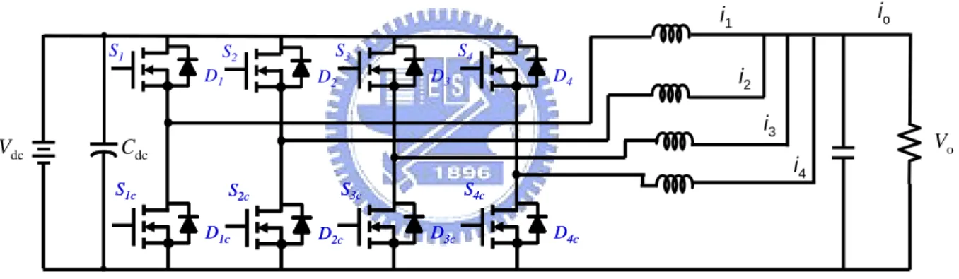
Cdc Vdc i1 i2 i3 io i4 Vo S1c D1c S1c D1c S2c D2c S2c D2c S3c D3c S3c D3c S4c D4c S4c D4c S1 D1 S2 D2 S3 D3 S4 D4
Fig. 1.1. Multiphase buck converter topology.
Fig. 1.1 is the four phases buck converter topology. Although increasing the number of phases lower the per phase current, it also results other problems such as circuit complexity, current sharing during transient response, and enlargement of PCB board area. A proper selection of the number of phases needs an engineering compromise between current per phase, switching frequency, circuitry complexity, size, and efficiency. The integration of the PWM controller with integrated MOSFET gate drivers poses another design issue in the design of high frequency high power density VRM controller. This solution benefits with a compact solution and lowers component counts. However, because there are four wires
needed for each phases, it also presents layout problem due to longer gate traces and limits its maximum switching frequency. Another disadvantage is that it also prevents the selection of other MOSFET for gate driver.
The evolution began since the high frequency processors were developed. The driven power comes down from less-than-5-volts to 1.2volts even 0.5 volts. The supplying current of 100 amperes for a 1.0 volts regulation within 10 millisecond settling time with a load current slew rate of 100 amps per microsecond requires the design of high power density VRM with fast dynamic responses [10].
1.2
R
ESEARCHM
OTIVATION ANDO
BJECTIVESThe more flexible solution is to provide a programmable and configurable digital VRM controller with design simplicity, application scalability, and optimized control architecture for a target design [11]-[13]. The design a digital VRM controller for multi-phase synchronous buck converter by using a novel interlaced sampling and control techniques is mentioned.
The multiphase interleaved PWM technology was applied on DC-DC power converter for a period of time [14]-[15], and it improved the output of the converter a lot. Using the modulation, the n times switching frequency with n phases interleaved DC-DC converter. That means we can raise the effective output frequency without raising on-off frequency of each phase switch [16] is obtained. Deadbeat control in digital system makes the transient be done in several clock cycles. In this paper, adopted deadbeat control is used to achieve better dynamic response.
Single chip is low cost these days, and it makes the digital control realization to be popular [17]-[18]. In some ways, the modern digital control technique is going to replace the traditional analog technique. The main purpose of digital control scheme is implementing the
digital close loop control by software, so that the single-chip is used to finish the work which may be done by complex analog devices. Field Programmable Gate Array (FPGA) contains the logic gates which are assembled by users to generate certain function circuit. Not only flexible, it gets high speed system clock so that the data computation is faster. The complex control theory can be implemented in FPGA with very high speed integrated circuit hardware description language (VHDL). The accuracy can be checked by simulation and the function can be modified the as hoped. As the result, there are many benefits if realizing the VRM controller with programmable digital system.
1.3
R
ESEARCHM
ETHOD ANDS
YSTEMD
ESCRIPTIONThe thesis presents the realization of digital VRM controller with multiphase-interleaved PWM technique by using FPGA. Fig. 1.2 shows the system architecture of the proposed single-chip FPGA solution for the digital control of a multi-phase synchronous buck converter. The supplying current to the microprocessor is equally shared by the multi-phase synchronous buck converters. Each phase of the DC/DC converter is fairly shifted with an equal shifted degree to reduce the current ripples feeding into the output capacitors bank. The power consumption of a target microprocessor is mainly determined by the activity factor when running a specific program.
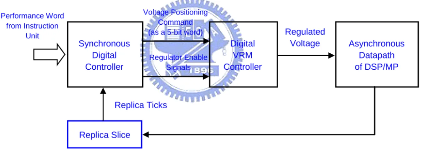
The current demanding depends on the execution of pipelined instructions which can be synchronized by a replica tick generated by a replica slice of the target microprocessor. Fig. 1.3 shows the system level diagram of a power management system for asynchronous data path of an advanced microprocessor. A synchronous digital controller is used to generate the voltage positioning command for a voltage regulation module (VRM) during dynamic power management process to maintain the microprocessor operating in an optimal condition. The current loading profile is used by the pipeline operation of a microprocessor. It is observed
i1 i2 i3 io i4 Vo Digital Command
Digital Control Block
Sensing & A/D Circuit Synchronous Sampling Signal Generator PWM Generator Cdc Vdc S1c D1c S2c D2c S3c D3c S4c D4c S1 D1 S2 D2 S3 D3 S4 D4
Fig. 1.2. Block diagram of a four-phase interleaved VRM buck converter with closed loop control. Synchronous Digital Controller Digital VRM Controller Asynchronous Datapath of DSP/MP Regulated Voltage Voltage Positioning Command (as a 5-bit word) Regulator Enable Signals Performance Word from Instruction Unit Replica Slice Replica Ticks
Fig. 1.3. System level diagram of a power management system for asynchronous datapath of an advanced microprocessor.
that the slew rate of the load current depends on the activity factor of each execution phase for a series of pipelined instructions. In order to provide a smooth power flow to the target microprocessor with fast dynamic response, a feed-forward control scheme is used to improve the dynamic response of a VRM regulator. The proposed digital VRM controller provides a feed-forward controller to speedup its dynamic response under large load current transients.
1.4
T
HESISO
RGANIZATIONSThis thesis presents the design a single-chip FPGA implementation of a digital VRM controller for multi-phase synchronous buck converters by using a novel interlaced sampling and control techniques. The dissertation is organized as follows. The fundamentals of multiphase interleaved buck converter are introduced in Chapter 2. The operation method, steady state analysis, and multiphase effect are reviewed.
In Chapter 3, the controller design way is presented. The voltage loop, current loop compensator and PWM controller are analyzed.
In Chapter 4, implementation of the digital VRM controller by using FPGA is described. It illustrates the digital controller implement method, including a mainly phase-shift PWM generator, a digital compensator, and an ADC synchronous sampling.
In Chapter 5, simulation and experimental results are given. Some conclusion and suggested future works related to this research are summarized and discussed in Chapter 6.
Chapter 2
Review and Analysis of VRM
2.1
M
ATHEMATICALM
ODELING OFV
OLTAGER
EGULATORM
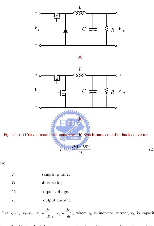
ODULEVRMs are considered as multiphase buck converter. The main function of buck converter is reducing the dc voltage. It can be treated as combination of ideal switches and low pass filter which was formed by inductors, capacitors and resistance. However, it’s impossible to find the ideal switches. By different architecture of practical realization, the buck converter can be separate into conventional one and synchronous rectifier one.
Fig 2.1(a) shows the conventional buck converter, it comes with a MOSFET and a diode. Fig 2.1(b) shows the synchronous rectifier buck converter, the other MOSFET is used instead of diode. The forward voltage of the diode is usually larger than MOSFET switching. VRMs work offer low voltage, and forward voltage of the diode will hinder the working of converter. So the rectifier synchronous is chosen one in the thesis. However, those 2 kinds of realization form just need one control signal source which determines the duty ratio of switches. Dead-time is required to prevent these two MOSFET from short-loop if the synchronous rectifier model is used.
The buck converter model can be derived with power plant small signal model. While the system operates under the continuous conduction mode (CCM), the inductor should be chosen as follows:
v
iv
oL
C
+ − + −R
(a)v
iv
oL
C
+ − + −R
(b)Fig. 2.1. (a) Conventional buck converter. (b) Synchronous rectifier buck converter.
o i s I V D D T 2 ) 1 ( − L≥ (2-1) where Ts sampling time; Dc duty ratio; Vi input voltage; Io output current. Let x1=iL, x2=vC, dt dx x dt dx L 2 2 1 ' , =
x1'= , where iL is inductor current, vC is capacitor
voltage. Considering the inductance equivalent series resistance rL and capacitor equivalent series resistance rC, we may get the flowing two equations:
) ( dt dv C i R C L − + r i dt di L v L L L i = + (2-2) C C C r dt dv C v + = ) C L dt dv C i R( − (2-3)
The equivalent series resistance is discussed because the current of VRMs are large enough to produce obvious voltage drop even on small resistance. The power loss from inductance ESR also causes the output voltage lower. After inducing the effect of switching duty ratio, the equation of system is derived with state space form:
i v L x x ⎥ ⎥ ⎦ ⎤ ⎢ ⎢ ⎣ ⎡ + ⎥ ⎦ ⎤ ⎢ ⎣ ⎡ ⎥ ⎥ ⎥ ⎥ ⎦ ⎤ 0 1 ) ) 2 1 C C C C L C L C r R C r R R R r R L R r R L r r Rr Rr x x ⎢ ⎢ ⎢ ⎢ ⎣ ⎡ + − + + − + + + − = ⎥ ⎦ ⎤ ⎢ ⎣ ⎡ ( 1 ) ( ( ) ( ' ' 2 1 (2-4)
from the state space equation. For duty ratio versus output voltage, the transfer function is shown as: 1 )] ( + + [ 1 ) ( ~( ) ~ 2 + + + ≅ R L LCs V s d s v i o s r r C C sr L C C (2-5)
The steady state gain of the buck converter is as follow:
L i o r R R D V V + ⋅ = (2-6)
2.2
B
ASICO
PERATIONALP
RINCIPLES FORV
OLTAGER
EGULATORM
ODULEVRMs are set to achieve the high power high current and better efficiency requirement of new generation microprocessors. The switches and inductors of buck converter are connected in parallel to form the multiphase topology. In ideal condition, each of the phases carries the 1/n of the total current of system, where n denotes the phase numbers.
can be reduced. The faster transient response can be achieved with increasing of the equivalent switching frequency.
2.2.1 Inductor Current Ripple
Assume the system works in CCM, for single-phase buck converter, the current ripple which is mean to peak value of total current could be express as:
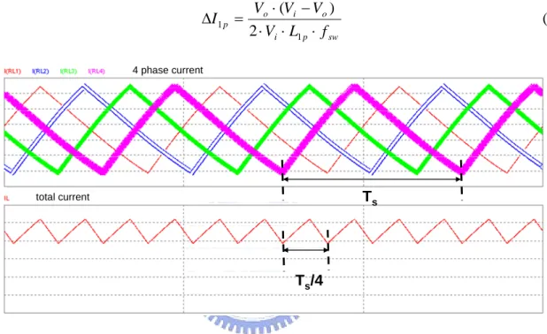
sw p i o i o f L V V V V ⋅ ⋅ ⋅ ⋅ − p I = 1 2 ) ( Δ 1 (2-7) 4 phase current total current Ts Ts/4
Fig. 2.2. Phase current and total current of four phases VRM.
where Vo is the output DC voltage, Vin is the input DC voltage, fsw is the PWM switching frequency, and L1p is the inductor of single-phase buck converter. Fig 2.3 shows the steady state current of four phases VRM. Four phases current which delay 90 degrees each other generate the total current with one 1/4 sampling time. The current ripple of n-phase interleaved VRM is as follows: n I f n V p sw p o i ) 1 L V V V I i o np 1 2 ( Δ = ⋅ ⋅ − ⋅ ⋅ ⋅ = Δ (2-8)
The output ripple current is much smaller than inductor current ripple than single phase. From (2-6) and (2-7), we know that the total inductor current of n-phase interleaved VRM can be
reduced by n.
The current ripple percentage is determined by the inductor value. Increasing the inductance value, the current ripple gets lowered. In opposition, lower the inductance will cause the more ripple current, more conduction loss, and lower efficiency. However, we may reduce the current ripple with smaller value inductor by using multiphase topology, so that we may use small inductor in parallel instead large inductor.
2.2.2 Output Voltage Ripples
In steady state, the output voltage is considered as a dc voltage with ripple. While the switching frequency is much larger than system natural frequency, the charging and discharging slope of capacitor voltage is0 approximated as constant.
The voltage ripple is caused by the current ripple, the relationship between charge, voltage, and capacitor value maybe written as:
C Q Vo p = Δ
Δ 1 (2-9)
And we may caculate the change of charge by integral the current ripple:
2 2 1 s L T i Q = ⋅Δ ⋅ Δ (2-10)
By (2-8) and (2-9) we may know output voltage ripple which is mean to peak value in single-phase buck converter could be express as:
2 1 ) ( sw p i o i o f C L V V V ⋅ ⋅ ⋅ 1 8 p o V V ⋅ ⋅ − = Δ (2-11)
while the output ripple of n-phase interleaved VRM is as follows:
2 1 2 ) ) n V f p o sw o 1 ( 8 ( n C L V V V V V p i i o onp Δ = ⋅ ⋅ ⋅ ⋅ ⋅ − ⋅ = Δ (2-12)
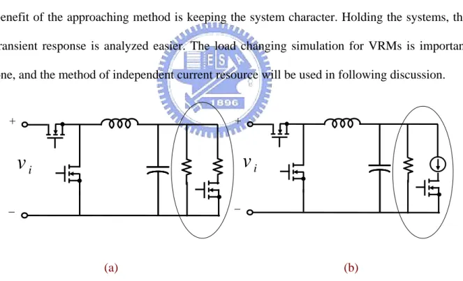
2.2.3 Load Changing Issue
There are several ways to approach the load changing condition, and two of them are the most popularly used. The first one is placing the resistance parallel with the load, and there is a switch to determine increasing of decreasing the load. Because of the output resistance influence the system transfer function, it’s hard for us to analyze the system. Fig 2.3(a) shows the parallel resistance load switching. A step load transient can be achieved by controlling the MOSFET. The change of resonant peak, quality factor…etc. makes the transient response can’t be predict simply by the transfer function.
The other way is placing another independent current source which is parallel with the load. Fig 2.3(b) shows the parallel independent current resource for load switching. The benefit of the approaching method is keeping the system character. Holding the systems, the transient response is analyzed easier. The load changing simulation for VRMs is important one, and the method of independent current resource will be used in following discussion.
v
i + −v
i + − (a) (b)Chapter 3
Digital VRM Controller Design
3.1
D
IGITALC
ONTROLS
TRUCTUREIn this chapter, the thesis describes the digital controller design of the VRMs. By using the compensator on current and voltage feedback loop, the desired out voltage is controlled well not only for steady state but also for transient. The multiple control loops is applied on the system to solve the problem. The inner loop is current feedback while the outer one is voltage feedback.
Besides feedback control, the thesis presents the feed-forward control scheme to improve the transient response. The current demand of processors depends on the working load which processors do. When the processor is going to execute the programs which need huge current, the power supply have to offer such current to processors in short period of time without changing output voltage a lot. However, the current demand for microprocessor becomes predictable because the execution of program is known. For the high frequency clock of digital system, it’s pretty enough to compensate the transient by the current demand feed-forward.
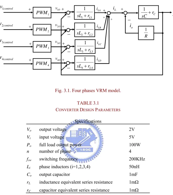
Fig 3.1 shows the four phases VRM closed loop control associated with output voltage feedback. The output voltage is sensed to compare with the voltage control reference. The inductor current of each phase will be placed after the voltage loop to solve the current sharing problem.
+ 1 1 1 L r sL + +rC sC 1 L i LA i + o
v
−
+ 2 2 1 L r sL + LB i−
+ 3 3 1 L r sL + LC i−
+ + 4 4 1 L r sL + LD i−
+ controlv
1 + + + + 1 PWM 2 PWM 4 PWM 3 PWM + O v1 O v2 O v3 O v4 controlv
2 controlv
3 controlv
4 oi
−
R 1Fig. 3.1. Four phases VRM model.
TABLE3.1
CONVERTER DESIGN PARAMETERS
Specifications
Vo output voltage 2V
Vi input voltage 5V
Po full load output power 100W
n number of phase 4
fsw switching frequency 200KHz
Li phase inductors (i=1,2,3,4) 50nH
Co output capacitor 1mF
rL inductance equivalent series resistance 1mΩ
rC capacitor equivalent series resistance 1mΩ
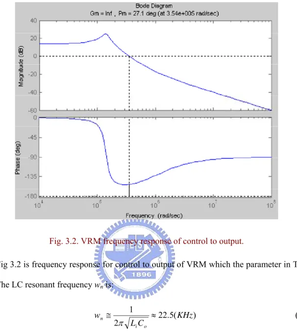
The design parameters of the constructed VRM are listed in Table 3.1. The equivalent switching frequency is raised to 800KHz by applying multiphase interleaved control method. By (2-5), the transfer function for control to out voltage can be written as:
1 10 2 5 10 10 5 5 ) ( ~( ) ~ 6 2 6 + × + + × − − s s s 11 × ≅ − s d s vo (3-1)
Fig. 3.2. VRM frequency response of control to output.
Fig 3.2 is frequency response for control to output of VRM which the parameter in Table 3.1. The LC resonant frequency wn is:
) ( 5 . 22 KHz Co ≈ 2 1 L w i n ≅ π (3-2)
which is sufficiently smaller than the equivalent switching frequency.
3.2
C
URRENTL
OOPC
ONTROL3.2.1 Current Loop Analysis
The current loop is the inner loop of the controller structure, and it is set to improve the dynamics transient response. In VRMs, the current loop plays an important role of whole compensator. Current demand of microprocessors change a lot in short time, so the current loop has to be designed well for transient. Otherwise, the current loop also resolves the part of current sharing problem and decreases the loss in the VRMs.
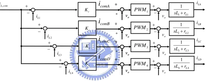
The current demand can be treated as feed-forward signal. Signal which comes from voltage controller is added with the feed-forward current demand, and the sum of the two signals is current command for each phase. Due to the prediction of current demand signal, we may make the transient shorter. Four current commands are sent to each phase to subtract to the inductor feedback current from ADC. The current error is compensated by the current loop gain KC, and then added with voltage feed-forward signal. The current loop can decouple the output voltage signal, and that makes the effect of load changing decreasing for output voltage. c K 1 L i − + c K 2 L i − + c K 3 L i − + c K 4 L i − + comC
i
comBi
comAi
comDi
1 1 1 L r sL + 2 2 1 L r sL + 3 3 1 L r sL + LA i LB i LC i LD i 4 4 1 L r sL + o v + + o v + + o v + + o v + + o v + + o v + + o v + + o v + + 1 PWM 2 PWM 4 PWM 3 PWM o v com L i , − + o v − + o v − + o v − +Fig. 3.3. Current loop control scheme.
Fig 3.3 shows the current loop control scheme where vcom is voltage compensation output and idem is the current demand signal from processors. Inductor feedback current of each phase is iLA, iLB, iLC, and iLD. The icom is the current loop compensation output.
3.2.2 Current Loop Controller Design
Deadbeat control method is used to achieve fastest step response. The deadbeat response only exists in digital control system. The concept of deadbeat response is driving all nonzero poles into zero in some n sampling periods, where n denotes the system order. Although the control signal will be large impulse if the sampling period is short, we can get the nice dynamic response by applying this method.
The ADC which converts the analog phase current into digital can be considered as a zero order hold (ZOH). The transfer function of ZOH is written as:
s e s G Ts h − − =1 ) ( (3-3)
where T denotes the sampling time. With the transfer function of inductor and ESR, the discrete time transfer function which derived by z transformation is:
) ( 1 Ts L r L Ts L r L L e z r e − − − − = 0 ) ( 1 )} 1 ( ) 1 {( ) ( L Ts sc r Ls s e Z z G − + ⋅ − = (3-4)
The closed loop pole can be placed to zero if the chracteristic function is equal to zero. That means: = s G Kc sc (3-5) +
From (3-3) the value of Kc which is designed in order to achieve deadbeat reponse can be calculated as: T L r T L r L c L L e e r K − − − = 1 (3-6)
Taylor series expansion is used to expand LT rL
e− term, and the value of T L rL
is small enough to ignore in high order terms. As the result, Kc can be approximatly caculated as:
T L
Kc ≈ (3-7)
With the current demand feed-forward and inductor current feedback, the current loop is mainly constructed. The gain of current is designed by the theory of deadbeat response. The next step is design of voltage loop which generates the signal and offers it to the current loop control.
3.3
V
OLTAGEL
OOPC
ONTROL3.3.1 Voltage Loop Analysis
The voltage loop is the outer loop which generates the compensation signal to inner control loop. It mainly improves the steady state response. The voltage loop may neglect the dynamics of inner current loop and treat it as constant while designing the voltage loop controller. The output voltage is used to not only feedback but also for feed-forward. The feedback signal is subtract by the voltage command, and the feed-forward is sent to compensator output of current loop.
1 1− − + z K vi vp K * o v + − o v current loop icom3 4 com i 2 com i 1 com i + C r sC+ 1 + + + + + + current demand feed-forward signal o i − R 1
Fig. 3.4. Voltage loop control scheme.
Fig 3.4 shows the voltage loop control scheme where vo* is voltage command given to determine the output voltage. Inductor feedback current of each phase is iLA, iLB, iLC, and iLD. The icom is the current loop compensation output. The controller on voltage loop is selected to be proportional-integral (PI) controller. In order to improve the transient response and reduce the steady-state error, the integral term is added into the voltage loop compensator. The value of Kvp is the result loop gain of the deadbeat response, and Kvi is the integral gain of voltage loop.
3.3.2 Voltage Loop Controller Design
Since the current loop may be consider as constant once the deadbeat control is applied, the controller of voltage loop could be easier designed. For the output voltage feedback and ADC, we may write the transfer function as:
) 1 ( − + = ⎟⎟ ⎠ ⎞ z C T rC 0 ) ( 1 ) 1 ( ) 1 ( ) ( ⎜⎜ ⎝ ⎛ + ⋅ − = − sC r s e Z z G C Ts sv (3-8)
The transfer function contrains output capacitor, capacitro ESR, and ZOH. Let the characteristic quation be zero:
=
s G
Kvp sv (3-9)
+
From (3-4) we may caculate the value of Kvp which is designed in order to achieve deadbeat reponse: C v r C T C K ⋅ − = (3-10)
The compensated signal goes through the current loop, and the feed-forward voltage is added beyond the current loop. The summation of feed-forward voltage and compensated current signal will enter the PWM generation block.
3.4
P
ULSEW
IDTHM
ODULATIONC
ONTROLThere are some ways to achieve pulse width modulation. There are trailing edge, leading edge, and dual-edge PWM by different carrier. Most PWM scheme contains sawtooth or triangular wave with comparator. No matter analog PWM generator or digital one, they transfer the signal into certain frequency rectangular wave with duty ratio.
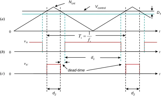
However, we have to choose the proper peak-to-peak amplitude, so that the reference signal could be modulated precisely. Fig 3.5 shows the dual-edge PWM and the dead-time setting.
0 0 vA vA ( )a ( )a ( )b ( )b t t 0 vA’ vA’ t ( )c ( )c d1 d2 d2 dead-time DT Ncnt Vcontrol s s f T = 1
Fig. 3.5. (a) Modulation Carrier. (b) Upper switch PWM waveform. (c) Lower switch PWM waveform.
Assume switching frequency is much higher than signal operation frequency, the reference may be considered as constant. Signals which go to two switches are generated by comparing the carrier wave and the reference signal. The equation for carrier and reference will be obtained as: cnt control s on N V T T D = = (3-11)
where D is the duty ratio of the PWM wave, Ton is the turn-on time of the upper switch without dead-time, Vcontrol is reference signal, Ncnt is the height of carrier wave, and Ts is the period of triangular wave. The signals of the two switches are complement. However, the dead-time is needed to prevent the two switches from conducting at the same time. Considering the dead-time, the modified duty ratio d1 is written as:
cnt control N DT V d1 = − (3-12)
digital number to determine the length of dead-time: time dead s cnt s T N DT T d D ⋅ = ⋅ − ) ( 1 (3-13) = −
Chapter 4
Implementation and Setup of the Digital VRM
Controller
4.1
A
RCHITECTURE OFD
IGITALVRM
C
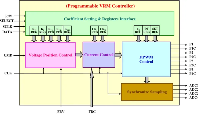
ONTROLLERThe design of the proposed VRM control scheme is based on FPGA. First, the overall system specifications should be defined to determine the design parameters, such as the system operating frequency, digital sampling frequencies, and the computational format of each control parameters. The realization for each control block of the proposed VRM controller is detailed described in this chapter. Fig. 4.1 shows the functional block diagram for the realization of the proposed digital multiphase interleaved PWM controller.
In order to avoid the switching noises and get the accurate averaged value of the inductor current, the sampling of the phase inductor current is triggered by its PWM signal on both leading and trailing edge to get the mid-point value on rising and falling slopes. The VRM control system consists of two major parts: current loop and voltage loop. The FPGA chip is used to realize the digital controller part which includes ADC sampling controller, the digital phase-locked loop, the digital loop compensator, the current sharing control structure and the digital PWM generator.
The compensator parts contain PI controller and lead controller for voltage loop. The programmable gain is place into current loop. Sampling of the PWM could be adjusted by the ratio of switching frequency and system clock. The phase shifter generates the interleaved signal which comes from PWM generator. Dead-time is designed to be settable to prevent the two switches conducting at the same time.
Coefficient Setting & Registers Interface
Voltage Position Control Current Control
SCLK DATA SELECT CLK P1 P1C P2 P2C P3 P3C FS REG (Programmable VRM Controller) KP REG KI REG KLK REG CKI REG CKD REG W R/ CMD KLA REG DT REG SET REG KLB REG P4 P4C FBC FBV ADC1 ADC2 ADC3 ADC4 Synchronize Sampling DPWM Control
Fig. 4.1. Functional block diagram of digital VRM controller.
4.2
I
MPLEMENTATION OFD
IGITALC
ONTROLLER4.2.1 Fixed-point Computation
The floating point computation is used to solve the mathematic problem in the computer. However, it cost more if the higher accuracy is desired. In computing, a fixed-point number representation is a real data type for a number which has a fixed number of digits before and after the radix point. Fixed-point number representation stands in contrast to the more flexible than floating point number representation.
Fixed-point numbers are useful for representing fractional values which are in native two's complement format if the executing processor has no floating-point unit or if fixed-point provides improved performance or accuracy for the application. Therefore, many low-cost embedded microprocessors and microcontrollers do not support floating point computation.
Based on the concept of fixed point computation, Q format comes to remarked the movement of the radix point and it is often used in hardware that does not have a
floating-point unit and in applications that require constant resolution. Q format is a fixed floating-point number format where the number of fractional bits is specified. For example, a Q10 number has 10 fractional bits. It can be treated as 10 bits movement of radix point.
In terms of binary numbers, each magnitude bit represents a power of two, while each fractional bit represents an inverse power of two. Thus the first fractional bit is , the second is , the n 2 / 1 4 /
1 th is , and so on. For unsigned m bits number which is defined Qn format, the maximum which it can present is 2
n
2 / 1
m-n-1, and the minimum non-zero number
which it can present is . If the signed bit is induced into computation, the positive bound range will be half, and the other half parts of number will be used to present the negative number with two’s complement. For example: a 12 bits signed number which is defined Q10 format, that means the radix point is between the second and third most significant bit (MSB), then the following number 011100000000 can be decomposed
n
2 / 1
0 1 . 1100000000 signed bit integer part fraction part
The number showed above is 1.75 with Q10 format. However, it looks the same as 1792 if the Q format is unknown. So the Q format definition is important during the fixed-point computation process.
4.2.2 Implementation of Proportional-Integral Controller
The adders and multipliers are basis of the compensator. With difference equation, the digital compensators are realized by combination of adders and multipliers. However, the bits length restricts the computation results of the adders and multiplier. The most common case is overflow of the multiplier result. In order to avoid this kind of problem, the maximum of the computation element is set. Considering of Q format definition, there is the problem of radix point to be shifted.
1
9
1
9
1
13
sign bit sign bit
sign bit
9
1
1
1
sign bit9
10 bits (Q0)4
2
22
saturation fraction (delete)
9
14bits(Q0) 10 bits(Q9)
Fig. 4.2. Multiplier results with saturation and Q format.
Fig 4.2 shows the multiplication of two sign bit number. One is 10 bits length number with Q9 format and the other is 14 bits length number without Q format. The output of the multiplication is restricted as 10 bits length sign number. With sign bit, there are 23 bits to show the result of multiplication. Due to the limit of bit length and Q format, the original output is changed into 9 bits number with sign bit instead. The fraction part of the 22 bits number is 9 bits, so they are deleted to make the final value into Q0 format. The left 13 bits have to be shorten to 9 bits, so the saturation is determined as the maximum and minimum number which can be presented with 9 bits.
The PI controller output is sum of a proportional gain term, P, and integration gain term, I. Each transfer function for each component is determined by its coefficient. The gain of P is set by the Kp coefficient. The range of Kp is 000000000000b to 111111111111b which provides a gain adjustment range of 0 (i.e., P component disabled) to 4. That means the Kp coefficient it set with Q10 format. This term applies a proportional gain to the error d(n). As the gain term is increased, the power supply responds faster to changes in d(n), but decreases system damping and stability. Step response overshoot and ringing could be caused by too
large a value of the gain term. The integral gain of I is set by the Ki coefficient. The range of Ki is 000000000000b to 111111111111b which is set into Q10 format. It provides an integrator gain adjustment range of 0 to 4. Unlike and main contribution of proportional gain (which reduces instantaneous error), integral gain reduces steady state error to zero. The integrator has infinite dc gain, and consequently adjusts the mean supply output voltage to drive its input to zero. The amount of time power supply takes to reach its steady state is inversely proportional to the integral gain Ki. If the value of the integral term is too large, it will cause oscillation and instability. On the other hand, too small of an integral gain can result in limit cycle oscillation.
In summary, while Kp is increased, stability is decrease, but the response time and steady-state error get improved. Increasing Ki decreases stability, improves response time, but worsens settling time.
vi
K
+ _ 12 12 12 vpK
1 −z
+ + 12 12 Compensator*
v
v
com ov
viv
Coefficient Registers
FSM_Based PI_Controller
Limiter CoefficientRegisters
idle
S1
S2
S3
S5
S4
Output Register Register Register CMD FB Delay Register Delay Register MUX MUX MUX ADDER MULTI If cs=‘1’If cs=‘0’ MUXMUX MUXMUX
Fig. 4.4. Hardware circuit schematic chart of compensator.
The digital PI controller can be derived from transformation of analog PI controller. There are some ways to digitalize the continuous transfer function. The forward method and backward method takes just one register to realize, while the bilinear method need two registers because of the numerator and denominator term need each to realize. The method mentioned in this paper is backward one. Discrete time transfer function of PI controller could be written as following: 1 1 ) ( − − + = z K K z G vi vp (4-1)
The differential equation of voltage PI controller with backward which is shown in Fig. 4.1 is: ) 1 ( ) ( * ) ( ) (n = K +K ⋅v n +v n− vcom vp vi vi (4-2)
where vvi(n−1) means data the at last sampling time spot.
Fig. 4.3 shows implementation structure of the PI controller. It takes register, adder, and multiplier to implement the PI controller block. To minimize circuit realization of the adder and multiplier, a scheduling strategy for realizing the compensator by using
finite-state-machine (FSM) is presented. The computing process of both control loops takes one adder, one unit delay register, and one multiplier. Furthermore, the control parameters can be tuned. The hardware circuit schematic chart of compensator is shown in Fig 4.4.
The limiter of the digital integral is designed larger with the decreasing order of integral constant. In order to keep accuracy of integral register, the boundary of limiter can be set to (2n/Kvi). However, the increasing of the limit boundary will raise the bit number to calculate during integral process. The limiter behind the adder of proportional gain and integral gain is the bit length limit of the size we designed. It’s set to be the same long as input so that we may series the control with others which offer certain function like phase lead compensation. The basic structure of voltage and current loop is by combination of PI controller, adder, multiplier and limiter. Fig 4.5 shows the state diagram of the deadbeat compensator. Pin definition is listed on Table 4.1.
×× ++ ×× LL ++ ×× ++ LL ++ S0 S1 S2 S3 S4 S5 S6 S7 S8 S9 S10 S11 Voref Vo Kvp IL_Lmt IL Kc PWMGInv Dlmt Io Vireg ×× Kvi ++ ++
TABLE4.1
PIN DEFINITION OF THE DEADBEAT CONTROLLER
Symbol Status Range Description
CLK W 1 / 0 eternal clock, max =
200MHz
RST W 1 / 0 controller reset
0:disable 1:enable
D_lmt[11..0] W 0~4095 duty limiter
Kc[11..0] W 0~4095 current loop gain
Kvp[11..0] W 0~4095 voltage loop
proportional gain Kvi[11..0] W 0~4095 voltage loop integral
gain
IL[11..0] W 0~4095 inductor loop
IL_lmt[11..0] W 0~4095 inductor current limiter
Vo[11..0] W 0~4095 output voltage
feedback
Voref[11..0] W 0~4095 voltage reference
Io[11..0] W 0~4095 output current
feedback
So[11..0] R 0~4095 controller output
The pin detail description is shown below:
CLK – system clock, which affect the computation delay of the process. It’s also the basic timing unit of finite state machine.
RST – reset of the controller register.
D_lmt – in order to avoid the power being overload, the duty has limit to be set if needed. Kc – gain of current loop.
Kvp / Kvi – voltage loop proportional / integral gain IL – inductor current feedback signal from ADC IL_lmt – limiter of feedback inductor current
Vo – output voltage feedback signal from ADC Voref – voltage command, reference of voltage loop Io – output current feedback signal from ADC So – controller output
4.2.3 Implementation of Lead Controller
The digital lead controller is designed as first order digital infinite impulse response (IIR) filter with programmable pole, zero, and DC gain. The transfer function of lead controller could be written as:
B z A z K z x z y z G − + = = ) ( ) ( ) ( (4-3)
There are two forms which are most frequently used to realize: Direct Form I and Direct Form II. Fig 4.6 shows the difference between them. Direct Form II implementation takes less delay unit than the Direct Form I. In order to realize the transfer function with adder, multiplier, and delay unit, we retrieve the difference equation from (4-3):
) 1 ( ) 1 ( ) ( ) (n =K⋅x n +A⋅x n− +B⋅y n− y (4-4)
B
y(n-1)
x(n-1)
A
S0
y(n)
x(n)
S1
S2
S3
K
Fig. 4.7. FSM flow chart of the first order IIR filter.
The first order IIR filter offers three coefficient to be adjusted, which are K, A, and B. It is a one-pole filter with pole coefficients of B and zero coefficient of A and a proportional gain term with coefficient of K. The transfer function is presented in (4-3). The range of A is 100000000000b to 011111111111b (in 2s complement). The coefficient A is set into Q10 format with sign bit, so it presented a pole which the range is from –2 to 2. The range of B is 100000000000b to 011111111111b (in 2s complement) and provides a pole adjustment range of –2 to 2. The range of K is 000000000000b to 111111111111b which is set into Q10 format. It provides a filter gain adjustment range of 0 to 4. This filter may be used as lead compensator, lag compensator, low pass filter, or high pass filter. The coefficient B controls the cutoff frequency of the pole. The coefficient A determined the replacement of the zero. Gain term K adjusts the dc gain of the compensator.
Finite state machine is used here again to implement the controller with less adder and multiplier. Fig 4.6 shows the state diagram of realizing the lead controller. The computing two registers to save the data of x(n-1) and y(n-1) if the Direct From II is used. Direct Form I needs two registers to hold the value of w(n) and w(n-1), too. The Fig 4.7 is implemented
with Direct Form II. The digital lead controller may be determined by bilinear transform from analog lead controller.
4.3
I
MPLEMENTATION OFD
IGITALP
ULSEW
IDTHM
ODULATIONG
ENERATORThe digital pulse width modulation (DPWM) module is a segment of digital hardware that provides the diverse gate control options necessary to drive the switching power supply device. The module can generate up to four pairs of signals (phases) accommodating pulse width and phase modulation schemes that can be modulated by hardware.
There are some practical methods from the literature (like counter-comparator, delay-line, and hybrid one, etc…) that can be used to generate digital PWM. The first method is used to realize the block in the thesis. The increasing of PWM frequency and resolution will require a very high clock frequency and imposes a design constraint both for high-frequency digital circuit design and cost.
Symmetric Reference Carrier (Triangular) VCMD SYMS Mux Comparator RST Dead-Time Generator PWM signal Frequency Divider DT FSW PHN Asymmetric Reference Carrier (sawtooth) Carrier Generator PHSH CLK Phase shifter
Higher switching frequency also companies with higher switching losses and electromagnetic interference. Therefore, it becomes a design trade-off between the required PWM switching frequency, control resolution, control scheme, and circuit topology. Interleaved PWM technique with phase-shift control has been developed for high-density DC-DC converter to enhance its current output capability in VRM applications. Phase-shift interleaved PWM scheme can effectively reduce the output ripple and distortion with lower switching frequency.
Shown in Fig. 4.8 is the proposed DPWM block diagram. The DPWM is designed to apply flexibility to different power applications. The interleaved phases, dead-time setting, symmetric or asymmetric reference carrier alternating, and PWM switching frequency, is designed as programmable. The maximum speed of DPWM can be clocked to 200MHz. The pin definition is listed in Table 4.2.
TABLE4.2
PIN DEFINITION OF THE PWMGENERATOR
Status Range Description
Clk W 0 / 1 Eternal clock, max = 200MHz
RST W 0 / 1 Reset ouput
0:disable output 1:enable output SYMS W 0 / 1 Symmetric selection
0:symmetric wave 1:asymmetric wave PHSH W 0 / 1 Phase shift
0:disable 1:enable
PHN[2..0] W 0~7 out put phase number = PHN+1 FSW[11..0] W 0~4095 Switch frequency = FSW/CLK DT[6..0] W 0~127 Dead-time = DT/CLK Vcmd[11..0] W 0~4095 PWM input signal PH1-PH4 R 0 / 1 PWM output signal
The pin detail description is shown below:
CLK – system clock, affects the counter period and switching frequency. RST – reset of the DPWM generator
SYMS – symmetric of the carrier type PHSH – enable of the phase shifter or not
FSW – counting number of the carrier, affects the switching frequency DT – dead-time which is programmable the length
Vcmd – comparison reference signal, which comes from controller output
PHn(C) – up to four pairs PWM waveform, PHn and PHnC are complement each other with dead-time
4.3.1 Implementation of Carrier Generator
The compensated duty cycle modulation variable is applied to the input of the DPWM through the DPWM input MUX. This MUX selects the mode which output will be or determine system management as the DPWM modulation source. The MUX input is connected to a pair of programmable symmetry selection circuits that can be used to latch the value of u(n) at a specified time. Selection of the symmetric type determines the basic form of the modulation. Once the symmetric one is chosen, it needs double time to count the carrier than asymmetric one. The DPWM generator offer leading-edge modulation, trailing-edge modulation, and dual-edge modulation. Leading-edge modulation and trailing-edge modulation belong to asymmetric reference carrier, while dual-edge modulation belongs to symmetric reference carrier.
From leading-edge modulation scheme, the better transient during load-adding event can be obtained, but not always responsive to load-releasing event. In the other hand, trailing-edge
modulation scheme is good for releasing transient while it can’t guarantee the load-adding transient event.
The leading-edge modulation and trailing-edge modulation needs different side sawtooth wave to implement. The increasing counter is used to implement the leading-edge modulation while the decreasing one is used for trailing-edge one. Dual-edge needs both increasing and decreasing counter and performs the carrier as triangular wave.
4.3.2 Implementation of Dead-Time Generator
Dead-time is designed to solve the problem of switch conduction at the same time. To prevent the turn on time and turn off time of the switches stacking, the PWM result duty is reduced a little.
Since the switch signal for the synchronous rectifier is complement each other, we may adjust the reference to generate dead-time. The signal of lower switch comes from comparison of reference and carrier wave. In order to generate the dead-time, we can’t complement the signal directly. The comparison result which reference equals to carrier should be modified.
The PWM signal comes from comparison between carrier wave and reference signal. If the carrier is made lower, the shorter of duty will be got. The loss of duty will become the dead-time. The reason of choosing shorten duty instead of lengthen the lower PWM is just preventing the lower MOS earlier off when the duty is near one. That way the upper MOS will keep switching while the lower one is off. Dead-time in this block is set to be the raising level of the carrier. The length of dead-time is set as:
M T N DT time dead s cnt ⋅ ⋅ = − (4-6)
Where Ncnt denotes the counting number of the carrier generator, Ts is the sampling time. The maximum of Ncnt is 4095 while the bit length is 12. M depends on the modulation type which
is chosen by carrier generator, M=1 while leading-edge or trailing edge, M=1/2 while dual-edge for two part of dead-time during one period.
4.3.3 Implementation of Phase Shifter
The switching frequency is programmed by the carrier counter and can be expressed as
cnt sw N clk f ⋅ = 1 (4-6)
where fsw denotes system output effective switching frequency, clk is digital system clock , and Ncnt means the number of the counting number.
PHN DPWM Divider FSW Delay Circuit PH1(C) PH2(C) PH3(C) PH4(C)
Fig. 4.9. Phase shifter circuit.
In order to shifter the phase in one period, the divider is used to calculate the degree to shift. However, four phase shifter doesn’t need the divider. Actually, four phase shifter may be realized with bit shifting and multiplier. When the least significant bit (LSB) is shifted out, the value will be roughly divided into 2 under fixed point calculation. Shifting the bit twice can get the quarter of the original value, and the three-forth value can be obtained with multiplier. For the three-phase one, we do need divider to count the value of shifting, and the multiplier is not required.
The DPWM timing generator provides up to four pairs flexible PWM or phase-shift which is modulated timing phases referred to as PH1(C) through PH4(C). Positive, negative, or system management processor-controlled dead times can be implemented. Each PHn output has its own pattern generator that can follow the computation result of the divider. The divider which determines the timing of shifting generates up to three values. Those values are the starting of the shifting while the first phase reaches it.
Fig 4.9 shows the circuit of the phase shifter, the shifting timing comes from the counting number and the phase number. The divider sends up to three values to the delay circuit. Once the value is reached, the output PHn(C) will be triggered to work, so that the shifted PWM waveform is obtained.
4.4
I
MPLEMENTATION OFS
YNCHRONOUSS
AMPLINGS
IGNALG
ENERATORThe synchronous sampling for inductor current of a switching converter plays an important role for the robust control of the current dynamics on a scale of its switching period. Peak current mode control scheme has been employed for the current loop regulation, however, it need a negative slope compensation to ensure stability when operating in high duty range and it also suffers from large discontinuity across the DCM boundary.
Fig. 4.10 shows the proposed interlaced sampling and control scheme. The sampling of the inductor current is synchronized with the leading edge of PWM signals for both turn-on and turn-off. The proposed sampling scheme have a high noise immunity to the common-mode switching noises induced by the switching of the MOSFET and its parasitic junction capacitances resulted by the heat sink. A true average current signal thus can be measured with accuracy within a switching period. The timing clocks for the digital controller and the digital PWM generator are interlaced with each other to achieve a minimum delay for a same
(a) (b) (c) (d) (e) (f) (g) (h) System Clock Control Clock Phase A PWM Phase B PWM Phase A Current
Phase A Sampling Signal
Phase B Current
Phase B Sampling Signal
Fig. 4.10. Two-phase synchronized sampling scheme.
sampling and switching frequency.
Fig. 4.11 shows an illustrative timing diagram of the synchronous sampling process. The rising and falling edge of the PWM switching signal is used to trigger a timer with a preset value of half of its switching intervals during both on and off periods. The average value of two samples are used as the instantaneous averaged value of the current sampling period and is used for the current regulation and current sharing control of the digital current controller. The fsw in Fig. 4.11 denotes system effective switching frequency. Rising / Falling sampling mode sample one each period, so that the sensed current looks like the digital signal with the frequency fsw. On the other hand, if we sample while both rising and falling the sensed current will be the signal with frequency 2 fsw. Table 4.3 is the pin assignment description of the interlaced synchronous sampling scheme. The active mode, phase number, symmetric type, and the sampling method could be chosen.
tt tt Signal PWM iL 0 Rising sampling Falling sampling
Rising & Falling sampling sw f 2 T Triangular waveform 0 sw f
Fig. 4.11. Hardware circuit of the interlaced synchronize sampling scheme.
TABLE4.3
PIN DEFINITION OF THE INTERLACED SYNCHRONOUS SAMPLING SCHEME
Status Range Description
CLK W 1 / 0 Eternal clock, max =
200MHz
RST W 1 / 0 PWM reset 0:disable 1:enable
ACT W 1 / 0 selection of "active high / active low" 0:Active low 1:Active high
PHAN[1..0] W 0~3 number of phase for output 00:1 phase 01:2 phase 10:3 phase 11:4 phase
SYMS W 1 / 0 selection of symmetry
for PWM 0:asymmetric 1:symmetric
FSW[11..0] W 0~4095 switching frequency REF1-REF4 W 0~4095 reference for each
SAMP[1..0] W 0~2 sampling method 01:rising sampling 10:down sampling 11:rising & down sampling
ADCI1-ADCI4
R 1 / 0 sampling trigger signal to ADC 1 1 11 11 1 1 CLK ADCI Mux 0 1 PHAN 0 Sync Register Q D DFF Q D DEF Q D DEF 1 0 1 0 1 0 SAMP Sync_sample controller A B A B FSW REF ACT Ref<Fsw=1
Ref<Fsw=1 StateState FSM S0 S1 3 2 12 12 12 12 1 0 1 0 A B A B A B A B A B A B 0.5 1 0 1 0 00 01 10 11
Fig. 4.12. Hardware circuit of the interlaced synchronize sampling scheme.
Fig. 4.12 shows the hardware circuit of the interlaced synchronous sampling scheme. The signal will be compared first, and then the ADC sampling signal will be generated at the middle of the trailing edge PWM. After selecting the sampling type, there are sampling signal for ADC which correspond the phase number.
The pin detail description is shown below:
CLK – system clock, the same as the DPWM generator, so that the same timing has been guaranteed.
RST – reset of the sampling signal generator
signal, so the output is designed into active high or low.
PHAN – phase number, the output will look upon the phase number to determine the shifting of sampling signal.
SYMS – asymmetric / symmetric, comes from DPWM carrier type. REFn – reference which goes to each phase
SAMP – sampling type, rising / falling sampling once each period, rising and falling type sampling twice, the changing timing of sampling signal is half of the carrier.
ADCn – sampling signal which goes to ADC
The relation between phase switching frequency and effective output ripple frequency can be written as:
swp
swt n f
f = ⋅ (4-7)
where fswt denotes the system output effective switching frequency, fswp is phase switching frequency, and n means the number of phase. The equation only stands while the phases are interlaced with 2π/n.
Chapter 5
Experimental Verification and Simulation
Result
5.1
V
ERIFICATION OFB
LOCK FORD
IGITALC
ONTROLThis simulation platform is based on integrated with the Matlab/Simulink and Modelsim simulation software. The Simulink not only simulates the digital signal processing, but also offers the simulation of the analog environment. Thus, we could quickly revise the errors and improve the result. The thesis used the c0-simulation block to set toolbox of Simulink and constructed a multi-phase synchronous buck converter. According to the VHDL language design, the ModleSim program is involved into the Simulink to implement digital controller. Therefore, the co-simulation can be done by setting parameter and system clock.
Realized with VHDL code
Simulink elements