國立交通大學
電子工程學系 電子研究所碩士班
碩士論文
複晶矽薄膜電晶體的充放電機制用於
記憶體應用之研究
A Study of Trapping/De-trapping Mechanisms in Poly-Si
Thin Film Transistors for Memory Applications
研 究 生:洪政雄
指導教授:林鴻志 博士
黃調元 博士
複晶矽薄膜電晶體的充放電機制用於記憶應用之研究
A Study of Trapping/De-trapping Mechanisms in Poly-Si
Thin Film Transistors for Memory Applications
研 究 生:洪政雄 Student: Cheng-Hsiung Hung 指導教授:林鴻志 博士 Advisors: Dr. Horng-Chih Lin 黃調元 博士 Dr. Tiao-Yuan Huang
國立交通大學
電子工程學系 電子研究所碩士班
碩士論文
A Thesis
Submitted to Department of Electronics Engineering & Institute of Electronics College of Electrical and Computer Engineering
National Chiao-Tung University in Partial Fulfillment of the Requirements
for the Degree of Master in
Electronic Engineering June 2008
Hsinchu, Taiwan, Republic of China
複晶矽薄膜電晶體的充放電機制用於記憶應用之研究
研究生:洪政雄 指導教授:林鴻志 博士 黃調元 博士國立交通大學
電子工程學系 電子研究所碩士班
摘 要
在本論文研究中,我們在複晶矽薄膜電晶體傳導特性中觀察到一種有趣的遲 滯(hysteresis)現象,並對此進行深入的探討。為了清楚的瞭解其發生的起因, 本研究針對可能調控此現象的參數,包括:通道厚度、通道長度、通道寬度、電 漿處理及溫度等,設計相關的實驗以解析其影響。根據實驗的結果,我們提出一 物理模型,利用複晶矽薄膜電晶體中晶界充放電機制,說明在特定條件下造成此 種遲滯現象的原因與過程。此外,本論文也探討不同材料與元件組態對於遲滯現 象的影響。我們的研究也同時評估,複晶矽元件之遲滯特性對於將來運用於記憶 體應用之可行性。A Study of Trapping/De-trapping Mechanisms in Poly-Si
Thin Film Transistors for Memory Applications
Student: Cheng-Hsiung Hung Advisors: Dr. Horng-Chih Lin Dr. Tiao-Yuan Huang
Department of Electronics Engineering and Institute of Electronics National Chiao Tung University, Hsinchu, Taiwan
Abstract
A new hysteresis phenomenon presenting in the current-voltage characteristics of
poly-Si thin-film transistors (TFTs) was discovered, for the first time, in our
experiments. Mechanisms reported in previous literatures fail to explain the finding.
To clearly understand the root cause of the hysteresis, we examine several factors that
might affect the phenomenon, including channel thickness, channel length, channel
width, post-metal treatment, and temperature, etc. From the results, we propose a
physical model, based on the trapping/detrapping events occurring in the grain
boundaries of poly-Si thin film transistors (TFTs), to reasonably explain the hysteresis
behavior of poly-Si TFTs. Besides, we also investigate the effects of Ge incorporation
in the channel and structural factors on the hysteresis characteristics. Our findings
Acknowledgment
經過兩年的努力,即使途中經過了不少阻礙與挫折,最後還是將這篇 論文給順利完成。在這過程中需要感謝的人太多,首先,我誠摯地感謝指 導教授林鴻志博士和黃調元博士,兩位老師細心的教導與要求,使我在人 生中最重要的兩年中累積到許多寶貴的經驗,感謝林博指導我正確的研究 方法與態度,讓我學習到更有效處理事情的態度,對於以後進入社會工作 受益很大。感謝黃老師對我論文的修改,使得論文更佳的完善。 再來,我要感謝帶我做實驗的蘇俊榮學長,對你一直覺得不好意思,你 為了帶我們做實驗,而沒將你的博士論文在你出國前寫完,真是對不起你 也非常謝謝你,由於你帶著我做實驗、量測與分析,並且無私跟我分享實 驗小技巧,讓我漸漸得以培養獨立思考的能力。此外,也要感謝 Benson、 林哲民、徐博、蔡子儀、阿森等實驗室學長,在實驗中對我的幫忙與電性 的討論,讓我在實驗上可以少走許多冤枉路。再來要感謝我們這批同梯碩 二戰友們,劉大偉、江忠祐、陳玲、洪文強、林漢仲、李冠樟、陳威臣, 跟你們一起做實驗真的很快樂,讓深夜作實驗時感覺不那麼可憐,我會永 遠記住你們的。也要感謝實驗室裡的碩一學弟妹,有了你們,讓實驗注入 新的活力也帶來更多的歡樂。另外謝謝生科所蕭程允、林志衡學長,跟你 們一起量測真的很開心,可以分享彼此的夢想。 最後,我要特別感謝我的父母親,洪文亨先生和張秀枝女士,感謝他們 對我教養與栽培,讓我無顧慮的專心求學,真是謝謝他們。我也要感謝我 的女朋友,黃郁閔小姐,陪伴我度過人生最精華的階段,一直給我很大支 持。 洪政雄 誌於風城交大 2008 年 6 月Contents
Abstract (Chinese)...i Abstract (English)………ii Acknowledgment……….iii Contents…...iv Table Captions...vi Figure Captions...vii Chapter 1 Introduction1-1 Overview of Semiconductor Memory………..1
1-1-1 1T-DRAM……….2
1-1-2 SONOS……….4
1-2 Overview of Nanowire Technology……….5
1-3 Motivation………7
1-4 Thesis Organization……….8
Chapter 2 Device Fabrication
2-1 Device Structure and Process Flow……….9
2-1-1 Planar Structure………9
2-1-2 Inverse-T Double-Gate NWTFT………10
Chapter 3 Electrical Characteristics of Planar TFTs
3-1 Observation of Hysteresis in polycrystalline silicon……….13
3-2 Measurement Setup for Electrical Characterization………..14
3-3 Effects of Poly-Si Channel Thickness………15
3-4 Effects of Plasma Treatments……….16
3-5 Effects of Bias Conditions……….18
3-6 Effects of Temperature………...19
3-7 Mechanism for the Occurrence of Hysteresis………20
3-8 Density-of-States (DOS) Extraction………..29
Chapter 4 Effects of Channel Materials and Device Structures on Hysteresis
4-1 Characteristics of Poly-SiGe TFTs……….35
4-2 Effects of Double-gated Configuration………..36
4-3 Basic Characteristics of Inversed-T-gated NW TFTs……….38
Chapter 5 Conclusion and Future Work
5-1 Conclusion……….42 5-2 Future Work………...43 References………...44 Figures……….54 Vita………...88 Publication List………...89
Table Captions
Chapter 1
Table 1-1 Features of embedded memories………54
Chapter 2
Table 2-1 Split conditions of bottom oxide thickness………60
Chapter 3
Table 3-1 Major performance parameters for poly-Si TFTs which received FG annealing 30min………...76
Table 3-2 Major performance parameters for poly-Si TFTs which received NH3
Figure Captions
Chapter 1
Fig. 1-1 Comparison between conventional one transistor/one capacitor (1T/1C) DRAM and capacitor-less one transistor (1T) DRAM………...54
Fig. 1-2 Operation principle of 1T-DRAM cell. (a) Excess holes accumulate in the body region at “1” state (low Vth). (b) Excess holes are swept out of the body region at “0” state (high Vth). (c) Id-Vg characteristics to represent (a) and (b) (not experiment data)……….55
Fig. 1-3 Comparison of memory cell cross-section between the floating gate structure and SONOS……….56
Fig. 1-4 (a) Schematic representation of VLS growth of Si nanowires. (b) Binary phase diagram for Au and Si illustrating the thermodynamics of VLS growth. [40]………56
Chapter 2
Fig. 2-1 Process flow of the conventional poly-Si TFT fabrication………..57
Fig. 2-2 (a) Top view and (b) cross-sectional view of the ITDG-NWTFT…………58
Chapter 3
Fig. 3-1 Transfer characteristics of TFTs with channel thickness 50nm under FS and RS modes………..61
Fig. 3-2 Transfer characteristics of TFTs with channel thickness 100nm under FS and RS modes………...61
Fig. 3-3 Transfer characteristics of TFTs with channel thickness 30nm under FS and RS
modes………...62
Fig. 3-4 Transfer characteristics of TFTs which received FG annealing 30min under FS and RS modes with different gate sweeping range: (a) VG=-3V to 6V,
and (b) VG=-3V to 8V. Characteristics of fresh device are also shown for
comparison………...63
Fig. 3-5 Transfer characteristics of TFTs which received NH3-plasma treatment
under FS and RS modes with different gate sweeping range: (a) VG=-3V to
6V, and (b) VG=-3V to 8V. Characteristics of fresh device are also shown
for comparison………..64
Fig. 3-6 Transfer characteristics with fixed and different under FS and RS modes………..65 min G V max G V
Fig. 3-7 Transfer characteristics with fixed and different under FS and RS modes………...66 max G V min G V
Fig. 3-8 Transfer characteristics of TFTs measured at different temperature under FS and RS modes………...66
Fig. 3-9 The energy band diagram of a partially depleted poly-Si channel under (a) flat-band (b) on-state (FS), (c) and on-state (RS). The two possible de-trapping paths for trapped electrons during RS period are also depicted and denoted as 1 and 2……….67
Fig. 3-10 The energy band diagram of a fully depleted poly-Si channel under (a) flat-band (b) on-state (FS), (c) and on-state (RS). The energy band structure along the channel direction is also illustrated in (d). The three de-trapping paths for trapped electrons during RS period are also depicted and denoted as 1, 2 and 3, although the path 2 is prohibited by the buried oxide………68
Fig. 3-11 Transfer characteristics of TFTs in linear scale for determining the threshold voltage………..69
Fig. 3-12 Transfer characteristics of 20 consecutive RS and FS measurements of a TFT with sweeping gate voltage range of (a) VG=-3V to 8V and (b)VG=-3V
to 6V……….70
Fig. 3-13 Calculated density-of-states as a function of surface band-bending………71
Fig. 3-14 (a) Transfer characteristics of a TFT under FS/RS mode. A pulse with gate voltage of 6 V is applied to the gate. The inset is the pulse form. R and G points represent the conditions corresponding to the reading of the two logic states if we set the read voltage at Vg = 0V, and P point represents the condition programming. (b) Evolution of drain current of a device before, during, and after the programming with different pulse width. The circled area in the figure is further illustrated in (c) in which the drain current is illustrated in log-scale………..72
Fig. 3-15 Retention characteristics of a programmed device characterized at room temperature and 85 ℃……….73
Fig. 3-16 Evolution of drain current for a poly-Si TFTs with L/W=0.4um/20um at VG=0V, VD=0.1V. “1” state is a programmed state with a gate pulse of 6V
and pulse width 1 sec, “0” state is obtained by erasing the device with a gate pulse of -3V and pulse width 1 sec………...74
Fig. 3-17 (a) Time dependence of transfer characteristics. (b) Retention time of TFTs
at VG=0V………..75
Chapter 4
Fig. 4-1 The width of hysteresis (H) as a function of channel length for different channel poly-Si and poly-SixGe1-x TFT devices………...77
Fig. 4-2 Comparisons between transfer characteristics of poly-Si and poly-SixGe1-x
TFTs……….77
Fig. 4-3 The width of hysteresis (H) as a function of channel width for poly-Si and poly-SixGe1-x TFTs………...78
Fig. 4-4 Transfer characteristics of TFTs with the same channel thickness (50nm) but different bottom oxide thickness. Note that all bottom gates are grounded in the measurements……….79
Fig. 4-5 Comparisons between transfer characteristics of TFTs with different bottom oxide thickness (a) TBox=20nm (b) TBox=50nm (c) TBox=200nm under
Fig. 4-6 Energy band diagram of the devices with (a) a thin and (b) a thick bottom oxide……….81
Fig. 4-7 Transfer characteristics of planar TFTs with different constant bottom gate bias under FS/RS mode………82
Fig. 4-8 The cross-sectional view of ITDG-NWTFTs taken by TEM. The circled area in (a) is expanded as shown in (b)………83
Fig. 4-9 Transfer characteristics of a planar TFT and an ITDG-NWTFT………….84
Fig. 4-10 Transfer characteristics of ITDG-NWTFTs under different operation modes……..……….84
Fig. 4-11 Hysteresis characteristics of ITDG-NWTFTs under MSG and SSG modes...85
Fig. 4-12 The width of hysteresis (H) as a function of channel length for planar TFTs and ITDG-NWTFTs……….85
Fig. 4-13 Transfer characteristics with gate voltage variation of ITDG-NWTFTs…..86
Fig. 4-14 Hysteresis characteristics of ITDG-NWTFTs under SSG mode of operation with different inverse-T gate bias……….87
Chapter 1
Introduction
1-1 Overview of Semiconductor Memory
The semiconductor market has been active for years. A significant portion of this
market is given by the semiconductor memories. Semiconductor memories are usually
classified into two major types: volatile and non-volatile memories. Volatile memories
(VMs) lose data as the power is turned off. Most types of random access memory
(RAM) fall into this category. RAM is further divided into dynamic RAM (DRAM)
and static RAM (SRAM). DRAM requires refresh action to prevent charge loss from
the storage capacitor through leakage current.
On the other hand, non-volatile memories (NVMs) can retain their stored
information even after the power is turned off. There are many kinds of NVMs,
including read only memory (ROM), mask read only memory (MASKROM),
programmable read only memory (PROM), electrical programmable read only memory
(EPROM), electrical erasable programmable read only memory (EEPROM), flash memory,
scaled accordingly. In this regard, traditional VMs and NVMs have encountered
certain problems. Fortunately, there are solutions to overcome these issues. For
DRAM of VMs, to maintain sufficient charge storage capability as cell area is reduced,
we can use high-k dielectric materials, such as Al2O3、Ta2O5 [1] , to replace the
dielectric of SiON in conventional DRAM capacitors, or use three dimensional
structures to increase the effective capacitor area. Recently, a new concept of a
capacitor-less 1-transistor dynamic memory (1T-DRAM) cell has been developed and
it provides another possible approach for cell scaling. The detail of 1T-DRAM will be
described in the next section. For NVMs, discrete-trap non-volatile memories, such us
NROM, SONOS, and nanocrystal memories, provide particularly attractive feature of
storing two bits per cell. This could help accelerate the effective scaling of NVM cells,
and allows people to effectively cope with the difficulties in scaling the gate stack of
traditional floating-gate VNM devices.
1-1-1 1T-DRAM
The demand for high density, large capacity, high speed, and low-power
embedded memories are more important for system-on-chip (SoC) application.
Embedded SRAM and embedded DRAM are the two types of embedded memories
large area because it requires six transistors consisting of two p-channel MOSFET
sand four n-channel MOSFETs. Moreover, it is increasingly more difficult to scale
down the 6T SRAM in consideration of matching among cell transistors. The latter,
which integrates one transistor and one capacitor (1T/1C) in a cell, has a small cell
size albeit slower operation speed. Nonetheless, one of the main issues lies in cell area
reduction is the requirement of non-scalable capacitance of around 30fF/cell for
maintaining sufficient operation margin.
Recently, a new concept of a capacitorless 1-transistor dynamic memory
(1T-DRAM) cell has been developed [2]-[12]. In this scheme, as shown in Fig. 1-1,
there is no demand for a complicate storage capacitor, implying that the cell is process
compatible with logic devices, in addition to a small area size. The features of these
embedded memories are summarized in Table 1-1. Usually the device is built with an
SOI MOSFET with its channel body floating. The memory information is stored in
the floating body of the transistor. We know that a change on substrate bias (VBS) may
result in the threshold voltage (Vth) shift [13]:
(
)
2 2 2 (1) s A th B BS B o qN V V C ε ψ ψ Δ = + −When the channel body is floating, excess carriers may be generated during device
By use of the Vth shift, two distinct I-V conditions specifying “1” and “0” states are
defined. Up to now, this concept has been demonstrated and realized on several
architectures: partially-depleted (PD) SOI MOSFET [2]-[3], fully-depleted (FD) SOI
MOSFET [4]-[5], MOSFET on bulk silicon [6], double-Gate SOI MOSFET [7],and
FinFET[8].
Figure 1-2 schematically shows the operation principle of 1T-DRAM cell. The
device is n-channel. Excess holes are generated by impact ionization [9] or GIDL [10].
These holes are stored in the floating-body and lead to an increase in substrate
potential and the resultant Vth shift according to Equation (1). The condition when
excess holes exist in the floating-body is specified as “1” state. On the other hand, the
excess holes can be swept out of the body by forward-biasing the body-drain junction,
and the device returns to the fresh condition denoted as “0” state.
1-1-2 SONOS
High density NVMs are in high demand in the mobile and mass storage media
market due to the low cost-per-bit needs. However, scaling-down of conventional
NVM with a floating gate (FG) structure is expected to face a humongous barrier
beyond 45-nm node due to strong interference effect and scaling limit in tunneling
structure has been widely developed aiming to overcome the disadvantages of FG
structure [15]. It differs from the floating gate device in that the injected electrons are
trapped and stored in the thin insulating silicon nitride (Si3N4) layer rather than the
thick conducting layer of polysilicon. Figure 1-3 shows a comparison of the
cross-section between the two structures. One of the advantages of the charge trapping
at Si3N4 layer in SONOS over the FG device is its better immunity to charge loss via
defects (oxide traps, pin holes) in the surrounding oxide [16].
The operation principles for both program and erase operations in SONOS structure are similar to those in FG structure. Namely, they can be divided into three mechanisms,
channel hot electron injection (CHEI) [17], Fowler-Nordheim tunneling (FN
tunneling) [18] and band to band tunneling (BTBT) [19]. The goal of these
mechanisms is to inject charged carriers to or extract those stored charges out from the
insulator layer of Si3N4. Because of the difference in the number of charges stored in
the Si3N4 layer, distinctly different electrical transfer characteristics can be defined to
represent the logic states.
1-2 Overview of Nanowire Technology
Moore’s Law states that the number of transistors on a chip doubles every 18
years. To sustain Moore’s Law, the device size must be continuously scaled down.
However, as the devices reach 32 nm and beyond, traditional scaling methods
performed on planar structure face more technological and fundamental challenges.
Increasing demand on the resolution of the exposure system and extremely high
process/tool cost push the conventional approach towards its practical limit [20]. The
use of alternative 3D device structures is a possible approach to relax the
aforementioned issues. Among the proposed nano-scale structures, Si nanowires
(NWs) possess great potential as the active components in future nanoscale devices.
Owing to its inherently high surface-to-volume ratio, tunable electronic transport
properties [21]-[22], good thermal conductivity [23] and optical properties [24], NWs
are attractive for many applications, including nano CMOS [25], memory devices
[26], NW TFTs [27], biosensors [28]-[29], photodetectors [30], lasers [31], etc.
The preparation of NWs can be classified into two approaches,
namely, ”top-down” and “ bottom-up”. The top-down approach usually requires
advanced lithographic tools such as deep UV steppers [25] and e-beam writers [32] to
generate NW patterns. Although top-down methods are well developed and mature for
mass production, these methods become increasingly costly and/or slow as feature
size moves deeper and deeper into the nanometer regime. A great deal of works has
microscopy methods [33], nanoimprint lithography [34], and transfer lithography
[35].
Unlike the top-down methods which define key nanometer-scale metrics by lithography, the bottom-up approach employs chemical reactions to synthesize NWs. Several techniques to synthesize NWs have been developed, including thermal evaporation [36], vapor-liquid-solid (VLS) method [37], laser ablation technique [38], solid-liquid-solid (SLS) method [39], and so on. The most popular one is catalyzed VLS methods. The VLS process is shown in Fig. 1-4 [40]. NWs can be synthesized in single-crystalline form with precisely controlled structures, diameters and lengths, chemical compositions and doping properties using this catalyzed VLS method. However, since the catalyst is usually metallic in nature, metal contamination is a great concern. In addition, the alignment and positioning of NWs represent other issues for mass-production.
1-3 Motivation
As mentioned earlier in this chapter, the charges are stored in the insulator layer
of Si3N4 for SONOS, or in the floating body for 1T-DRAM to define the logic states.
Recently, while studying the electrical transfer characteristics of polycrystalline
silicon (Poly-Si) thin-film transistors (TFTs), we discovered accidentally a
phenomenon similar to that described for the operation of SONOS and 1T-DRAM,
albeit obviously of different mechanism. The purpose of this study is to investigate
evaluate its potential in practical memory applications.
1-4 Thesis Organization
The organization of this thesis is divided into five chapters. A brief overview of
semiconductor memory and nanowire technology is given in this chapter. In Chapter 2,
we briefly describe the device structures and process flow for fabricating the test
structures, including planar and nanowire devices. In Chapter 3, the hysteresis
mechanism is described and discussed, and the electrical characteristics as well as
program/erase characteristics of planar structure with poly-Si channels are
investigated. Effects of several factors including channel thickness, bias conditions,
temperature, and plasma treatment, are also investigated and analyzed. In Chapter 4, a
comparison of device characteristics between planar and nanowire structure,
characteristics of double-gate configurations, and influences on hysteresis windows
including channel materials, channel length and width, geometry effect, bias condition
effect , are investigated and discussed. Finally, a summary of conclusions achieved in
Chapter 2
Device Fabrication
2-1 Device Structure and Process Flow
In this chapter, we will introduce two kinds of TFTs structures, i.e., planar and
nanowire inverse-T gate structure, and describe the fabrication process in details.
2-1-1 Planar Structure
The process steps for the fabrication of planar poly-Si TFTs are illustrated in Fig.
2-1. First, a 100nm-thick in-situ n+ poly-Si layer was deposited on 6-inch silicon
wafers to serve as the bottom electrode (Fig. 2-1(a)). Then, a SiO2 layer of 20 nm, 50
nm, or 200 nm, respectively, was deposited by low-pressure chemical vapor
deposition (LPCVD) to serve as the bottom dielectric according to the split conditions
shown in Table 2-1. Next, a 30 nm, 50nm and 1000 nm-thick amorphous-Si (a-Si)
layer was individually deposited by LPCVD, followed by a solid phase crystallization
(SPC) step performed at 600oC in N
2 ambient for 24-hours to transform the a-Si into
and subsequent etching. This is followed by the deposition of an LPCVD oxide layer
of 20nm to serve as the top gate dielectric. A 100nm-thick in-situ-doped n+ poly-Si
was then deposited and patterned to serve as the top gate electrode (Fig. 2-1(c)).
Phosphorous S/D doping was implanted with a dosage of 15cm
5 10× -2 at the energy
of 35KeV (Fig. 2-1(d)) with the top gate serving as the self-aligned mask. A 350
nm-thick TEOS oxide by LPCVD was then deposited to serve as the passivation layer
(Fig. 2-1(e)). Finally, the fabrication was completed after the formation of test pads
using standard metallization steps (Fig. 2-1(f)). In this work we also characterized
poly-Si1-xGex TFT which are provided by Mr. Kai-Hsiang Chang, also of our research
group. The fabrication processes are similar to what we had described above except
for the use of a poly-Si1-xGex channel and the skip of the bottom electrode formation.
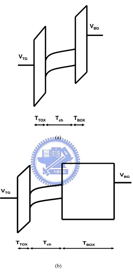
2-1-2 Inverse-T double-gate NWTFT
These devices are provided by Mr. Hsin-Hwei Hsu of our group. Top views and
cross-section views of inverse-T double gate NWTFT are shown in Fig. 2-2. The
process steps for the fabrication of these devices are illustrated in Fig. 2-3. First,
6-inch silicon wafers capped with 100 nm-thick SiO2 were used as the starting
substrates (Fig. 2-3(a)). Then, a 150 nm-thick in-situ n+ poly-Si layer was deposited.
and subsequent dry etching steps to fabricate the inverse-T gate structure (Figs. 2-3(b),
(c)). Note that the first etch step removed 100nm-thick poly-Si layer to form the upper
part of the inverse-T gate. While the remaining 50nm-thick poly-Si outside the
inverse-T gate regions was completely removed in the second etch step. A 20nm-thick
SiO2 was grown on the inverse-T gate by LPCVD to serve as the gate dielectric. Then,
a 100 nm-thick a-Si layer was deposited by LPCVD. Next, an annealing step was
performed at 600oC in N
2 ambient for 24-hours to transform a-Si into poly-Si (Fig.
2-3(d)). Subsequently, S/D implant was performed by P+ implantation at 15 keV and
cm
15
5 10× -2 (Fig. 2-3(e)). Note that the implant energy was sufficiently low so that the
implanted dopants were mostly distributed near the top surface of the poly-Si layer.
Then, S/D photoresist patterns were formed on the substrate by a standard lithography
step. A reactive plasma etch step was subsequently employed to remove poly-Si layer
except at the S/D regions and the nanowire channels were simultaneously formed in
this step in a self-aligned manner (Fig. 2-3(f)). Note that the etching time was
carefully controlled to make sure that only two NW channels remained on the corner
of inverse-T structure and the channel size was determined by various over-etching
time. Afterwards, the S/D dopants were activated by an annealing treatment. Then, a
20nm-thick SiO2 was deposited by LPCVD to serve as the top gate oxide.
serve as the top gate electrode (Fig. 2-3(g)). A 200nm-thick TEOS oxide was then
deposited by LPCVD to serve as the passivation layer. Finally, the fabrication was
Chapter 3
Electrical Characteristics of Planar TFTs
3-1 Observation of Hysteresis in polycrystalline silicon
Several hysteresis phenomena have been reported and discussed in many
reports [41-44]. In these reports, the origin of the hysteresis could be due to the
trapping of charges inside at the gate dielectric layers. In our study, accidentally, we
found that such phenomenon may also occur to certain poly-Si thin-film transistors
(TFTs). An example is shown in Fig. 3-1. Gate voltage (Vg) follows A-B-A
sequence, as indicated by the arrows shown in the figure. The loop is anti-clockwise.
In the following, “forward sweeping (FS)” refers to the sweeping of gate voltage from
negative to positive, and “reverse sweeping (RS)” means an opposite direction
sweeping. But such hysteresis phenomenon can not be explained by the mechanisms
identified in the previous reports [41-44]. As mentioned previously, the hysteresis
caused in the operation of SONOS is due to electron trapping and de-trapping events in
the Si3N4 trapping layer. But the electron trapping causes a positive shift in Vth,
other hand, the operation of 1T-DRAM shows similar anti-clockwise loop. However,
its mechanism is also not suitable for explaining our experimental results. The reason
is that the operation principle of 1T-DRAM relies on impact ionization [9] or GIDL
[10] to generate the excess holes accumulating in the floating body of the SOI channel.
This is obviously not the case in Fig.3-1, in which a small drain voltage of 0.1V is
applied. In this situation, the excess holes generated by impact ionization [9] or
GIDL [10] are not feasible.
3-2 Measurement Setup for Electrical Characterization
Before go into the investigation of the hysteresis phenomenon, we first describe
the measurement setup and definition of several electrical parameters in this section.
Electrical characteristics of fabricated devices are mainly characterized by the
automated measurement setup constructed by an AglientTM 4156A semiconductor
parameter analyzer and Interactive Characterization Software (ICS) software. During
all measurements, the temperature was controlled at a stable value by
temperature-regulated hot chuck.
Based on the transfer characteristics measured at Vd=0.1V, the parameters of the
TFTs including field-effect mobility (μFE), threshold voltage (Vth), subthreshold
Here, the field-effect mobility (μFE) is determined by m FE OX d Lg WC V μ =
where is the maximum transconductance and is the gate oxide capacitance per
unit area.
m
g COX
The threshold voltage (Vth), calculated by the constant current method, is defined
as the gate voltage (Vg) need to achieve a drain current (Id) of (W/L)× 100nA, i.e.
@ 10 th g d W V V I 0 An L = = × ,
where L and W are the channel length and width respectively.
The width of the hysteresis (H) in this thesis is defined as that the shift of Vth
between the FS and RS transfer curves, i.e.
FS RS th th
H =V −V .
Finally, the subthreshold swing (S.S.) can be calculated from the subthreshold
current in the weak inversion region by
(
)
. . log g d V S S I ∂ = ∂3-3 Effects of Poly-Si Channel Thickness
To more deeply understand the origin of the hysteresis in the poly-Si TFTs, we
designed several splits of experiments and investigated the effect of various device
characterized in the thesis received no post-metal treatment such as NH3-plasma or
H2/N2 mixed gas anneal. So in the following sections, unless we particularly
investigated the effect of post-metal treatment, the presented results were obtained
from devices without post-metal treatment.
First, we changed the channel thickness (Tch) to understand whether the different
Tch would influence the hysteresis formation or not. Figure 3-1, 3-2, and 3-3 show the
transfer characteristics of poly-Si TFTs with Tch of 50nm, 100nm, and 30nm,
respectively. It can be obviously seen that the hysteresis phenomenon exits in the
poly-Si TFTs of Tch=30nm and Tch=50nm, but not in the device with Tch=100nm
devices. From the results, we can infer that the channel thickness plays a key factor to
affect the hysteresis characteristics.
3-4 Effects of Plasma Treatments
The electrical properties of poly-Si TFTs are very different from the traditional
MOSFETs. This is due to the presence of abundant grain boundaries and defects in
TFTs, which result in large threshold voltage (Vth), poor subthreshold swing, low
mobility, and high leakage current. It is well known that post-metal treatments
effectively reduce both the tail and deep defect states inside the bandgap [45-51], and
treatment methods such as forming gas annealing (denoted as FG) in furnace [45],
plasma treatments in hydrogen or other ambient such as NH3 [46], N2/H2 [47], H2/O2
[48]or deuterium [49], high pressure of water vapor treatment [50], or water
passivation [51]. By these approaches, defects like dangling bonds at grain boundaries
and oxide/channel interface are passivated. As a result, the performance of TFTs
improves, including lower subthreshold swing, higher on/off ratio, and higher carrier
mobility.
In this work, we employed FG annealing in furnace and NH3 plasma treatment in
PECVD to investigate the effect of post-metal treatment, respectively. For the case of
FG annealing, the devices were exposed in N2/H2 (5%) ambient at 400oC for 30
minutes. For the case of plasma treatment, the devices were put in a diode NH3
plasma with RF power of 200 watt at 300oC for 1 hour.
Figure 3-4 shows the transfer characteristics of the devices which received FG
annealing. After annealing the device exhibits improved performance in terms of
better subthreshold swing, larger on-state current. Moreover, the hysteresis window
disappears after FG annealing, as observed in Fig.3-4 (a). The major performance
parameters for the FG annealing are listed in Table3-1. When applying larger gate
voltage range (in this case Vg=-3V~8V), we found that the hysteresis appears again
annealing, as observed in Fig.3-4 (b). This is ascribed to the relatively low
concentration of H2 species in FG annealing, or the strength of certain passivated Si-H
bonds is not strong and will be broken when the gate voltage is sufficiently high. To
demonstrate this conjecture, we also employed NH3 plasma treatment in PECVD for
1hr. The diffused hydrogen and nitrogen species have been reported to more
effectively passivate the trap states of poly-Si film. The transfer characteristics of the
devices, which received NH3 plasma treatment in PECVD for 1hr, are shown in
Fig.3-5. Similar to the case of FG annealing, improvement in device performance is
observed after the plasma treatment. The device parameters are list in Table3-2.
However, the hystersis window disappears even under high gate voltage bias (see
Fig.3-4(b)). From the results, we can infer that the post-metal treatments and different
bias condition may play another role in influencing the hysteresis phenomenon.
3-5 Effects of Bias Conditions
From the results we observed in previous sections, we got some hints that
different gate sweeping range ( ) may have influences on the hysteresis
window. Figure 3-6 shows the results for the gate voltage dependence of hysteresis
window in poly-Si TFTs. Transfer curves were measured by applying gate voltages
from -3V to a various maximum voltage ranging from 3 to 9V. It appears that, with
min, max g g
increasing gate voltage, the transfer characteristics of RS are shift negatively and
widen the hysteresis window. Moreover, in Fig.3-6 (b), it is seen that when the
applied gate voltage reaches or larger than a specific value (around 8V in the case),
the window width of hysteresis would saturate. Figure 3-7 also shows the measured
transfer curves by applying the gate voltages starts at a value ranging from -5, -3, to
-1V, and stop at 6V. It is seen that the transfer characteristics of RS curves of the three
conditions coincide together; however, the transfer characteristics of the three FS
curves are diverse. The outcomes are very dissimilar to the results as observed in
Fig.3-6. To briefly sum up, and have different effects on the transfer
characteristics of FS and RS. Therefore, the range of the gate voltage may also a
factor to influence the formation of hysteresis.
min g
V Vgmax
3-6 Effects of Temperature
Up to now, we have already obtained a few clues which would cause the
hysteresis phenomenon. To be worthy of noting, the former measurements were all
done at room temperature. In this section, we further investigate the temperature
dependence of hysteresis to acquire more information about the formation of
hysteresis. Figure 3-8 depicts the transfer characteristic curves measured at
increases the off-state leakage and narrow the hysteresis window. It is also observed
that the subthreshold swing of FS curves increases with increasing temperature, but
opposite trend observed for the RS curves. The results clearly evidence the
effectiveness of temperature in affecting the hysteresis.
3-7 Mechanism for the Occurrence of Hysteresis
Up to now, the hysteresis phenomena have been observed under some
circumstances discussed in our previous sections. Four important observations are
summarized as follows:
(Ⅰ) The hysteresis phenomenon occurs as the poly-Si thickness is sufficiently thin.
(Sec.3-3)
(Ⅱ) The hysteresis phenomenon occurs if poly-Si TFTs skip the post-metal treatments
such as FG annealing and NH3 plasma treatment. (Sec.3-4)
(Ⅲ) The window width of the hysteresis and the subthreshold characteristics of FS
and RS depend on both maximum and minimum sweeping gate voltage
( min, max). (Sec.3-5)
g g
V V
(Ⅳ) Window of the hysteresis shrinks as the measurement temperature increases
(Sec.3-6).
poly-Si TFTs. However, this is reasonable based on the above observations. First most
of papers reported previously studied the poly-Si TFTs with channel thickness around
or thicker than 100nm [52]. In some papers the channel thickness is indeed around or
thinner than 50nm, but the hysteresis phenomenon is still lacking [53, 54]. This is
attributed to the process sequence of device fabrication. In order to obtain
high-performance poly-Si TFTs, it is necessary to reduce the trap-states of the
polysilicon films. As a result almost all previously published works [45-51] employed
the plasma treatments to passive the defects in polysilicon films. Hence, it is hard to
discover the formation of hysteresis.
In this section, a model is developed to explain our interesting finding in poly-Si
TFTs. The electrical properties of poly-Si TFTs are different from the traditional
MOSFETs. This is due to the presence of grain boundaries (GBs), which result in
large threshold voltage (Vth), lower mobility, and high leakage current. Consider an
n-channel poly-Si TFT. Assume that the GBs run perpendicular to the channel and no
intentional channel doping is performed. So we limit our discussion to a device with a
doping concentration below the critical value of N* (N*=N
T/Lg), in which NT is the
concentration of traps located at the GBs, and Lg is the grain size. The presence of the
active traps at GBs provides deep-level trap sites for both electrons and holes and
height is proportional to the defect density (NT) at GBs and to the inverse of the
electron concentration (n) induced in the channel by the gate bias [55]. When the gate
voltage is gradually applied, the surface potentialΦ should vary along not only the
film depth but also the channel direction. Although the electrostatic distribution is a
three-dimensional problem, for the purpose of calculating its transport properties, it is
sufficient to treat the problem in one dimension as the channel length and width are
much larger than the grain size. The associated Poisson equation has been analyzed
and calculated [55, 56]. Levinson et al. [57] proposed a model for carrier transport
based on Seto’s [55] theory. In this model, the current is governed by thermionic
emission above the GBs’ barrier height, and drain current (Id) and the gate bias (Vg)
are related with the following relation:
3 2 ( ) exp( ) (2), 8 ( ) where 2 T d o ox G th ds s o ox g th eff s o s th s FB ox q N t W I C V V V L kTC V V qN V V C μ ε ε ε ε φ φ = − − − = + + (3), 2 and T (4). eff D g qN N N L = +
area; t is the thickness of the channel layer; Vth is the threshold voltage, and is
specified in terms of the effective doping Neff and the surface potential Φs. ND is the
concentration of shallow donors, Vg and Vds are the gate voltage and drain voltage,
respectively. The equation is valid in the subthreshold regime of the transistor.
According our experimental results, the dissimilar transfer characteristics between FS
and RS curves which form the hysteresis window can be attributed to the different
trap densities of GBs (NT) in the opposite sweeping direction. The Vth of FS is larger
related to RS as observed in Fig.3-1. This implies that the trap densities at GBs under
FS (NTFS) are higher than that under RS (NTRS). From equations (2) and (3), we can
understand that under the same gate voltage condition, the drain current of FS (IdFS) is
smaller than RS (IdRS) due to different NTFS and NTRS.
To turn on an n-channel poly-Si TFT, the traps under the quasi-Fermi level in the
depletion layer of the surface channel need to be filled by the electrons. This explains
why the Vth of poly-Si TFT is larger than traditional MOSFET. Normally, during the
RS process, the trapped electrons at the GBs should be immediately de-trapped from
the trap sites so that the transfer curve will follow the FS curve and hystersis does not
exist. An example is shown in Fig.3-2 for the device with 100 nm-thick poly-Si
channel layer. On the other hand, hysteresis is obviously observed for the devices with
FS process may retain in the trap sites during the RS process, resulting in a lowering
in the Vth and the formation of hysteresis. According to one of our previous
publications [58], the depletion width (Wdep) was estimated to be around 60nm for
poly-Si layers formed with a scheme identical to this work (e.g., SPC at 600oC in N 2
ambient for 24-hours). Correlating this with results of Figs.3-1 ~3-3, it is clear that
Wdep plays a key role for the occurrence of hysteresis. When the channel thickness is
smaller than Wdep in the channel, the channel becomes fully depleted as the device is
turned on; conversely, when the channel thickness is larger than Wdep in the channel,
the channel is partially depleted, and in the channel outside the depletion region the
potential is not disturbed by the gate voltage, so this region remains neutral. The
energy band diagrams for fully and partially depleted conditions at flat-band and
on-state modes under FS, and RS is illustrated as shown as Fig. 3-9 and 3-10.
In the case of partially-depleted case (Tch>Wdep), under the process of FS, the
energy bands near the semiconductor surface are bent downward ( Fig.3-9 (b)). In the
neutral region ( x>Wdep ), there are many empty trap states at the GBs with levels
distributed in the energy band gap. Nevertheless, in the depletion region ( x<Wdep ),
most of the trap sites under the Fermi level are filled with the induced electrons.
Subsequently, when the RS operation is executed and the bending of the energy band
In the meantime, the trapped electrons tend to de-trap from the trap sites. Three
possible de-trapping paths are identified in the figures. The first path (the path 1
denoted in Fig.3-9 (c) and Fig.3-10 (c)) is that the trapped electrons at the GBs are
released from the trap site to the conduction band by the thermionic emission. The
second path (the path 2 denoted in Fig.3-9 (c)) is that the trap-to-trap conduction via
the traps located in the neutral region of GBs, and then the electrons move to the
neutral region would recombine with holes therein. Consider the energy barrier for
paths 1 and 2, we find that energy needed for path 1 (~ 1/2 Eg for deep levels) is
bigger than that for the path 2, thus path 2 is more feasible. The third path (as denoted
in Fig.3-10 (d) as path 3) is that the de-trapping of electrons to the intra-grain region.
Similarly, it requires a sufficiently high energy for the electrons trapped in the deep
levels to leave. Since the path 2 is feasible and efficient as discussed above, we
believed it is the major de-trapping path, and the transfer curve under RS operation
can promptly follow the FS curve and eliminate the hysteresis, as observed in the
devices with a thick poly-Si channel (e.g., Fig.3-2).
In the case of fully-depleted mode ( Tch<Wdep), the path 2 is hindered by the
buried oxide, however. So the available de-trapping paths are paths 1 and 3, both of
which require a sufficient energy (or a period of time to acquire the energy) to occur
well explains why the hysteresis we observed in the devices with Tch=30nm (Fig.3-3)
and Tch=50nm (Fig.3-1).
We can examine the above model by extracting the trap density. If the model is
correct, portion of the traps (i.e., those deep states trapped with electrons) become
inactive during the RS process. Assume the amount of charges in those inactive traps
is QT (Coul/per unit area), the effective trap density in RS case, NTRS, is smaller than
that in FS mode, NTFS , with the following relation:
(5). T TFS TRS Q N N q = +
For poly-Si TFT, the subthreshold swing (SS) is affected by the effective trap
density, NT, with the following equation [59] :
ln10 1 ln10 1 where (6). T S ox T T t ox C C kT SS q C C kT C q N q C ⎛ + ⎞ = × × +⎜ ⎟ ⎝ ⎠ ⎛ ⎞ ≈ × × +⎜ ⎟ = × ⎝ ⎠
where CS is the capacitance of interface states at the channel/oxide interface, which is
usually negligible in poly-Si TFT. For the results shown in Fig.3-1, the SS are around
460mV/dec and 370mV/dec for the FS and RS I-V curves, respectively. Such
difference becomes reasonable with the inference of (5) to (6): SS is reduced owing to
the existence of inactive trap states. According Eq.6, an inactive trap density,
(equal to T N Δ T Q q ), is extracted to be 12 2 1.61 10 /x cm .
according to the following relation: ( ) (7). R F T th th th ox Q V V V C − = Δ = −
With this relation, we can approximately estimate the amount of the trapped charges
exist during the RS measurement. We used two ways to define the Vth, one is the
constant-current method described in Sec.3-2; the other is the intercept of gate voltage
of the linear drain current-Vg plots. For the results shown in Fig.3-1, the threshold
voltage defined by constant-current method (Vth Vg@Id W 100nA L
= = × ) for the FS
and RS curves are =1.41V and =-0.21V, respectively. The is thus
estimated to be around
F th
V VthR ΔNT
12 2
1.46 10 /x cm . The linear-Id vs. Vg plot is shown is Fig.3-11.
The extracted threshold voltage is =1.83V for FS mode and =0.29V for RS
mode, and is calculated to be around
F th V VthR T N Δ 1.66 10 /12 2
x cm . The results based on the
threshold voltage difference are very well consistent with that obtained with SS
difference 12 2
1.61 10 /x cm . These estimated values are also close to that reported in the
literature [55-57].
In Sec.3-4, we have discovered that the post-metal treatments have strong
influence on the hysteresis. When the devices received post-metal treatments such as
FG annealing and NH3-plasma treatment, the deep-level trap density NT is expected to
be reduced due to the defect passivation mechanism. The hysteresis window is thus
In Sec.3-5 section, we found that variation in the gate sweeping range
( ) may have effects on the transfer characteristics of FS and RS, as well
as the hysteresis window. By means of our model, we can further realize the effects of
and . According our measurement sequence, the sweeping follows the A-B-A
sequence as shown in Fig.3-1. FS (A to B) “programs” the device by filling the
deep-level traps with electrons and the amount of the stored charges is determined by
the . From this argument, it becomes reasonable to understand the results
illustrated in Figures 3-6 (a) and (b). The increase in hysteresis width with increasing
is attributed to the increase in the number of electrons trapped in deep levels,
since a higher may result in a higher band bending and the amount of deep
levels under the Fermi level in the channel would increase accordingly.
min and max g V Vg min g V Vgmax max g V max g V max g V
On the other hand, to erase the programmed device, the gate voltage applied in
the RS event must be sufficiently low to render an upward band-bending in the
channel, so that the stored electrons can be effectively expelled out from the stored
sites. Thus the extent of erasing is determined by . In Fig.3-7, transfer curves of
a device with fixed but various are measured. We can see that the RS
curves coincide due to the fixed . However, the used in the second
sweeping (-3V) is not sufficiently low to complete wipe off the stored charges in the
channel, so the third sweeping starting at -1V shows a smaller threshold voltage in the
min g V max g V Vgmin max g V Vgmin
FS curve as compared with the former two sweeping.
Figure 3-12 shows the transfer characteristics of devices under consecutive 20
times of measurements following the A-B-A cycles. In Fig.3-12 (a) and
are 8V and -3V, respectively. It can be seen that there exists a positive shift in the
transfer curves with increasing cycle (indicated by the arrow). This is attributed to the
degradation caused by the high . This issue could be solved by reducing the
. An example is shown in Fig.3-12 (b), the shift is transfer becomes negligible as
the is reduced to 6V. max g V Vgmin max g V max g V max g V
3-8 Density-of-States (DOS) Extraction
The electrical properties of polycrystalline semiconductor devices are strongly
affected by defects such as dangling bonds and strained bonds located at the GBs or
inside the grains. A comprehending of the intrinsic, energy distribution, density, and
behavior of these defects is important for development of polycrystalline TFTs.
Therefore, characterization and analysis of the density of gap states (DOS) in the
poly-Si is essential for understanding the devices characteristics. Moreover, accurate
DOS is required for the device modeling and simulation of poly-Si TFTs. In this
regard, there are several methods to determine DOS in polycrystalline devices such as
conductivity [62], and field effect conductance (FEC) [63] method, etc. Owing to the
fact that the FEC method could be directly applied to the TFT structure characterized
in this study, we adopt the technique to determine DOS. First the transfer
characteristics of both FS and RS are measured as a function of temperature, as shown
in Fig.3-8. The flat-band voltages then can be obtained using temperature method
with equation 8 [64]. 2 log 1 1 1 ... (8). 2 ox s s g ox o q q d G O dV t qkTN kT kT ε ⎡ ⎛ ψ ⎞ ⎛ ψ ⎞ ⎤ ≅ ⋅ ⎢ + ⎜ ⎟+ ⎜ ⎟ ⎥ ⎝ ⎠ ⎝ ⎠ ⎢ ⎥ ⎣ ⎦
From the above equation, the flat-band voltages can be determined as the VG
when log g d G T dV ⎛
⋅⎜⎝ ⎠⎞⎟ is temperature independent. Once the flat-band voltages are
obtained, the relationship between gate voltage Vg and surface potential,ψs, could be
established by incremental method [62] with the following relation
, , 1 , 1 , , (9). exp 1 g i FB s i i i ox s i s i s i o ox Si V V G G d q G t KT ψ ε ψ ψ ψ ε + + − − − = + ⋅ ⋅ ⋅ ⎛ ⎞ − ⎜ ⎟ ⎝ ⎠
Finally, the DOS of a given energy inside the band gap related to the surface
potentialψscan be expressed as follows:
(
)
2 22 0 2 (10) Si F s x s d DOS E q dx ε ψ ψ ψ = ∂ ⎛ ⎞ + = ⎜ ⎟ ∂ ⎝ ⎠The extracted DOS results of FS and RS are shown in Fig.3-13. It is observed that the
difference in the mid-gap regime. As the previous literatures reported, the deep-level
states are primarily contributed by the silicon dangling bonds locating at the GBs
[45,61]; while the tail states are ascribed to strained bonds or structure disorder near
the grain boundaries or interface of semiconductor and oxide [65, 66]. However, the
tail and deep states have different effects on the performance of transfer
characteristics. Deep-level states dominate the property of the subthreshold regime
such as subthreshold swing and Vth, while tail states control the above-threshold on
current regime such as on current ( ION ) and mobility. This is because the Fermi level
at the channel is in the proximity of the mid-gap in the subthreshold region, whereas it
is closer to the edge of the conduction band above the threshold. The results of DOS
are shown in Fig.3-13, it is clearly seen that under the operation of FS and RS, the tail
trap states are almost equal, but the deep states have significant difference. This can
reasonably explain the hysteresis phenomenon observed in this thesis. In Fig.3-10, the
electrons trapped in the tail states are easy to escape via path 1 or path 3 since their
energy level is close to the conduction band. Based on the results shown in Fig3-13,
we conclude the difference in trap density between FS and RS, i.e. NTFS and NTRS,
3-9 Program/Erase Characteristics
Further, the shift of the Vth for Vg increase and decrease, i.e., a hysteresis in the
transfer characteristics has been observed and can be translated into memory effects
for the application of the memory devices. To investigate its feasibility in this aspect,
we also study the characteristics of programming/erasing operation, and identify the
retention property, which a measure of the ability that a memory cell can retain the
stored information (or the charges in the present case).
In this section, we employed two approaches for the purpose of programming and
erasing operations. One is applied with a pulse of high voltage to the gate, and the
other is to sweep the gate voltage from a low value to a sufficiently high value for
programming, and vice versa for erasing, similar to the procedure shown in Fig.3-7.
First we investigate the P/E characteristics using the gate-pulse method. The
transfer characteristics of a test device under FS and RS modes are shown in Fig.14(a).
Here we select the reading gate voltage at 0V, and the two corresponding points in the
FS and RS curves as denoted as Q and R, respectively, in Fig.3-14 (a). We also set the
gate pulse with high level, VgH (=charging voltage), to 6V, and low level (VgL) to 0, as
shown in the inset of Fig.3-14 (a). Figure 3-14 (b) shows the time dependences of
drain current (ID) (in linear scale) of the device applied with pulse width tw=1, 0.1,
programming current under static case. Since it is not easy to tell the major difference
among the cases having different pulse-width, we further illustrate results of the first 9
seconds Fig.3-14 (c) by expressing the drain current in log-scale. The current
difference before and after the gate pulse programming operation becomes clear, and
such difference depends on the pulse width applied. When the pulse width reduces,
the discrepancy between two states lowers. It is even negligible as the gate pulse
shrinks to about tw=1ms. This is owing to the fact that the device structure has not
been optimized, and thus the programming is actually limited by the high RC time
delay due to the significant parasitic resistance and capacitance components contained
in the device (and, likely, the measurement instruments).
Figure 3-15 shows the results of retention by monitoring the drain current at
reading voltage of 0V at room temperature and 85 ℃. The programming pulse gate
voltage is VgL=0V, VgH=6V, and pulse width is tw=1 sec. Obviously, the retention is
significantly degraded as the temperature is raised. According to our model shown in
Fig.3-10, the trapped electrons at GBs are easy to escape via path 1 or path 3 at high
temperature, owing to the increase in thermal energy. Figure 3-16 shows the time
dependence of drain current under the alternate programming and erasing operation.
Two distinct logic states with different reading current are clearly illustrated in the
The next we investigate the P/E characteristics with sweeping gate voltage
method. As shown in Fig.3-7, portion of the stored electrons would remain in the trap
sites if the gate voltage of the RS curves stopped at a value larger than the specific
voltage for completely discharging the traps (around -3V in the present case). This
hints that the stored electrons could be retained in the channel for a period of time
unless a discharging at =-3V is applied for effective discharging (erasing). By
this mechanism, we can simply program our devices to “1” state (with a low threshold
voltage) by means of single sweeping of gate voltage along the forward direction to a
high gate voltage (e.g., 6V in the present case), and erase the device with RS
operation to a low voltage (-3V in the present case)). Such P/R cycles form complete
anti-clockwise loops in I-V characteristics in the range between and .
Figure 3.17 (a) depicts the transfer characteristics of a programmed device. It is seen
that the transfer curve is different from the fresh state, owing to the sweeping voltage
range starting at -1V. Figure.3-17 (a) also shows the time dependence of transfer
characteristics. We can see that the transfer curves are gradually approaching the fresh
stat. This can be explained that the charges loss with time. The time dependences of
drain current (I min g V min g V Vgmax
d)@Vg=0 shown in Fig.3-17(a) is plotted in Fig.3-17 (b). Distinct
difference between the programmed state and fresh state is still observed after 2400
Chapter 4
Effects of Channel Materials and
Device Structures on Hysteresis
In Chapter 3, we put our focus on the hysteresis phenomenon of planar poly-Si
TFTs. In order to further examine our model for the hysteresis and understand the
potential of such mechanism for practical applications, we now consider the effects of
channel materials and device structures on hysteresis in this chapter.
4-1 Characteristics of Poly-SiGe TFTs
Several previous reports have addressed the effect of Ge incorporation on device
performance [45, 67, 68]. In this section, we will not discuss the details of basic
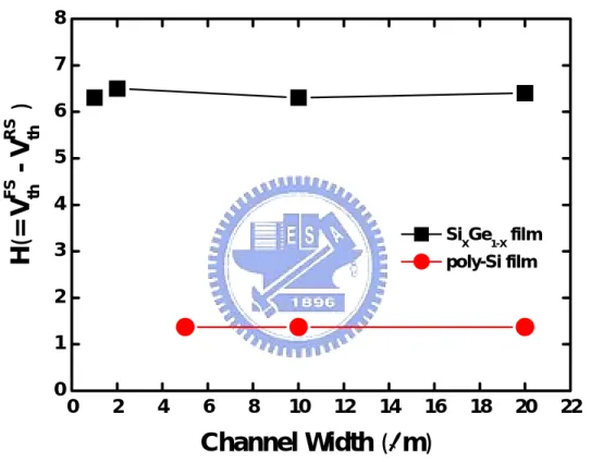
electrical characteristics of poly-Si1-xGex devices. Instead, we will compare the width
of hysteresis window between the poly-Si and poly-Si1-xGex TFTs. As shown in
Figure 4-1, in which the width of hysteresis (H) of the two splits of device is shown as
a function of channel length (L). Both splits have the same channel thickness (50 nm)
figure is 20μm and 5μm for poly-Si1-xGex and poly-Si devices, respectively. As can
be seen in the figures, the variation in channel length has no influence on H. This is an
indication of uniform trap density (NT) along the channel. However, we discovered
that the poly-Si1-xGex TFTs exhibit larger H over the poly-Si ones. This is attributed to
the fact that the incorporation of Ge atoms would introduce a considerable amount of
trap density [45, 67, 68]. Actually this would dramatically degrade the device
performance, including worse subthreshold swing, higher threshold voltage, larger
leakage current, and lower field-effect mobility, as observed in Fig.4-2. As a result,
the numbers of electron trapped in the deep-levels of a poly-SiGe channel in the FS
operation would be far more than that of poly-Si devices, resulting in a larger
hysteresis window.
Figure 4-3 depicts the H of the devices as function of channel width. Channel
length of the devices characterized in this figure is 2μm and 0.4μm for poly-Si1-xGex
and poly-Si channel layers, respectively. The effect of channel width on the hysteresis
window depicts a similar behavior to the channel length effect.
4-2 Effects of Double-gated Configuration
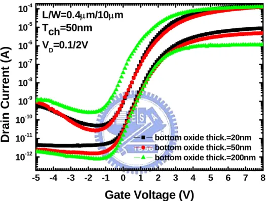
The transfer characteristics of the double-gated devices with split conditions listed
It can be seen that when the bottom oxide thickness decreases, the drain-induced
barrier lowering (DIBL) becomes less severe. This is ascribed to the use of a thinner
bottom oxide thickness that more effectively suppresses the field penetration from the
drain to the channel, resulting in a better control over the short- channel-effect, as has
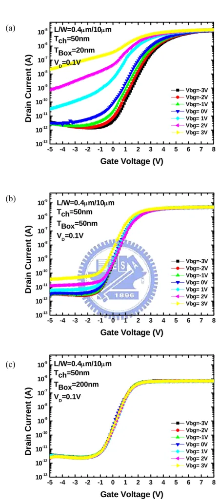
been demonstrated in previous papers [69-71]. Figure 4-5 describes the effects of
bottom-gate bias, VBg, on the transfer characteristics of the DG devices. It is
obviously seen that, when TBOX is thinner, VBg has a stronger influence on the transfer
characteristics. This can be understood by the band diagrams of the DG
configurations shown in Fig. 4-6. When the bottom oxide is thinner (Fig. 4-16 (a)),
the variation in VBg would change the field strength in the bottom oxide more
significantly and draw a more significant effect on the channel potential as well as the
performance parameters such as Vth and SS. On the other hand, if the bottom oxide
thickness is thicker (Fig.4-6 (b)), the variation of bottom oxide field by the VBg is
smaller, and results in negligible change in the device characteristics.
Figure 4-7 displays the hysteresis characteristics of a DG device by executing the
FS and RS operation to the top gate while a specific voltage ranging from -3 to 3 V is
applied to the bottom-gate. The bottom oxide is 20 nm for the device. It is seen that
the hysteresis window shrinks as the VBg is positive. From the transfer curves the
interface due to the positive VBg. In the RS mode, the bottom channel also serves as a
path for the de-trapping of the electrons trapped in the channel. As a consequence, the
window becomes smaller.
4-3 Basic Characteristics of Inversed-T-gated NW TFTs
The fabrication of the NW devices is described in Chapter 2. The cross-sectional
transmission electron microscopic (TEM) image of a device with inverse-T gate is
shown in Fig.4-8. In the figure, it can be clearly seen that the location of the NW
channels is precisely on the upper-step corners of the inverse-T gate. The perimeter of
the triangular NW channel can be characterized in the enlarged view of the NW
shown in Fig. 4-8 (b). Lengths of the three edges are 20nm, 30nm and 40nm,
respectively. Fig.4-9 compares the transfer characteristics of NWTFTs with those of a
conventional planar self-aligned device. Note that the drain current has been
normalized to the channel width. The results indicate that the shrinkage of channel
dimensions could help improve device performance in terms of higher on-current and
steeper subthreshold swing and better control of short-channel effect, which can be
ascribed to the increase in surface-to-volume ratio. The inverse-T double-gated (ITDG)
-NWTFT can be operated in several operation modes, including single-gated (SG)
MSG and SSG. MSG is to apply the sweeping gate bias to the inverse-T gate
electrode while the top-gate is grounded, and vice versa for the SSG mode. In DG
mode, both the inverse-T gate and top-gate electrodes are connected together and
applied with the sweeping gate bias. The transfer characteristics of ITDG-NWTFT
operated in these modes are shown in Fig. 4-10. In the figure, it can be clearly seen
that the DG mode shows better electrical characteristics, including steeper
subthreshold swing as low as 165 mV/dec. (@Vd=0.1V) and higher on-state current,
as compared with SG modes. This could be ascribed to its better gate controllability
and larger conducting width. The subthreshold swing for MSG and SSG modes are
253 mV/dec and 313 mV/dec, respectively. This indicates that the inverse-T gate has a
better gate controllability. Plasma damage induced during the formation process on
the outer surface of the NW next to the top-gate is presumably another factor
responsible for the worse subthreshold swing of the SSG mode.
To investigate the hysteresis characteristics of the ITDG-NWTFTs, we apply the
gate voltage respectively to the different gate electrodes, i.e., top gate and inverse-T
gate. Figure 4-11 shows the results of an ITDG-NWTFT under SSG and MSG modes
of operation. It can be seen that he hysteresis phenomena are observed. Because the
channel thickness of ITDG-NW is sufficiently thin, the NW channel is fully depleted,