整合於超大型積體電路標準單元設計流程的低功率技術
53
0
0
全文
(2) 整合於超大型積體電路標準單元設計流程的低功率技術 An Implementation of Integrable Low Power Techniques for Modern Cell-Based VLSI Designs. 研 究 生:李明崇 指導教授:闕河鳴. Student:Ming-Chung Lee Advisor:Dr. Herming Chiueh. 博士. 國立交通大學 電信工程學系碩士班 碩士論文. A Thesis Submitted to Institute of Communication Engineering College of Electrical Engineering and Computer Science National Chiao Tung University in Partial Fulfillment of the Requirements for the Degree of Master of Science in Communication Engineering September 2005 Hsinchu, Taiwan. 中華民國九十四年九月.
(3) 整合於超大型積體電路標準單元設計流程的 低功率技術. 學生:李明崇. 指導教授:闕河鳴. 國立交通大學電信工程學系碩士班. 摘要. 隨著 VLSI 技術的不斷進步,功率消耗逐漸變成一個亟需解決的問題。同時, 由於降低工作電壓使得漏電流在 CMOS 奈米製程中漸漸宰制了總功率消耗,因 此如何有效的控制功率消耗以及抑制漏電流(Leakage)現象成了在奈米製程中相 當重要的課題。在這一篇論文之中提出了使用目前可應用的電子自動化 (Electronic Design Automation)軟體分別實踐電壓分離(Voltage Separation),基極偏 壓(Body Bias),和功率閘(Power Switch)三項低功率電路技術。藉由電子自動化 軟體的協助,這些低功率技術可以有效地快速整合至標準單元設計流程 (Cell-Based Design Flow)中。利用電壓分離,適合的電壓可以分配到對應的功能 單元(Functional Unit)中,以避免提供過高的電壓導致過剩的功率浪費。基極偏壓 利用偏壓電晶體(Transistor)中的基極(body)以調整啟動電壓(Threshold Voltage), 因為漏電流多寡與啟動電壓呈指數反比關係,所以可藉由調整適合的啟動電壓值 控制漏電流大小。功率閘主要是在電路與供應電壓源之間的串接一個電壓開關, 當電路進入閒置時,功率閘將開啟以切斷於供應電壓源之間的連接,由一些文獻 中得知功率閘對於漏電流可以達到有效的抑止。藉由將低電壓技術整合於實體設 計流程(Physical Design Flow),可以實現帶有低功率技術特徵的電路。因此,此 篇論文提供了可利用標準胞元設計流程實現低功率電路技術的設計雛型。論文之 中所有的驗證跟設計都是使用 TSMC 0.18um 製程技術在實體設計流程中實現。. i.
(4) An Implementation of Integrable Low Power Techniques for Modern Cell-Based VLSI Designs Student: Ming-Chung Lee. Advisor: Dr. Herming Chiueh. Institute of Communication Engineering National Chiao Tung University Hsinchu, Taiwan 30050. Abstract As the scaling of VLSI process technology in this end of Moore’s Law era, power dissipation and power density have become an important issue. At the same time, voltage scale down make leakage power gradually dominates the total power consumption in nano-scale CMOS technology. Therefore, how to control power consumption and diminish the leakage power is essential in nano-scale process. In this thesis, we implement three low power techniques, which are Voltage Separation, Body Bias and Power Switch, utilizing existent EDA tool. Using the benefit which is provided via EDA tool, these low power techniques can be integrated into cell-based design flow rapidly. By using Voltage Separation, each functional unit can be feed with appropriate voltage level and avoid the excess power consumption from over-supply voltage. Body Bias uses biasing the body terminal of transistor to adjust the threshold voltage. Because the magnitude of leakage current has a exponential relation with threshold voltage, reducing leakage current is possible by increase of threshold voltage of transistor. Power switch is connecting power supply source series with a transistor. When circuit is in idle mode, the power switch is disconnected from power supply source. A significant reduction on leakage current can be achieved via power switch. By embedding low power techniques into physical design flow. A design circuit with low power technique feature is available. Therefore, this thesis provides an opportunity to realize several low power techniques relied on Cell-Based method. All implementation and verification within this thesis is used TSMC 0.18um technology in physical design flow.. ii.
(5) 誌謝 首先,論文可以順利的完成,首先要感謝我的指導教授闕河鳴博士,老師總 在於研究遭遇瓶頸的時候不辭辛勞的給予寶貴的指導以及建議,讓我在碩士論文 的研究過程之中平順許多。另外老師在平日培養學生獨立研究能力以及正確的科 學求知態度更讓我獲益匪淺,學生由衷感激。 另外,我要感謝偉閔、漳源、庭瑋、芳如。這兩年來的點點滴滴點綴了我的 碩士生涯,每次跟你們一起挑燈夜戰的日子會是我最美好的回憶。另外特別感謝 偉閔給我的研究題目許多意見,讓我的研究更趨完備。我也要感謝我的朋友們跟 兄長,跟你們一起度過的休閒時光是我可以持續努力不懈的最好調劑。 最後我要感謝我的父母,在我遭遇低潮的時候給我沒有止盡的愛和關懷,我 想讓你們知道論文能夠順利完成,其中有一部分的原因是因為你們的支持鼓勵, 讓我有繼續努力的動力。謝謝你們。. iii.
(6) Content: Chapter 1 Introduction ............................................................................1 1.1 1.2. Introduction............................................................................................1 Organization...........................................................................................4. Chapter 2 Background .............................................................................5 2.1 2.2 2.3. Voltage Separation.................................................................................5 Body Bias...............................................................................................8 Power Switch .........................................................................................9. Chapter 3 Implementation.....................................................................12 3.1 3.2 3.3. General Automatic Physical Design Flow...........................................12 Physical Design Flow for Voltage Separation .....................................15 Body Bias for Cell-Based Design Flow...............................................18. 3.3.1 3.3.2 3.4. Body Bias with Dual-Supply Standard Cell ........................................18 Body Bias with General Standard Cell ................................................21 Power Switch Implementation.............................................................24. Chapter 4 Implementation Results .......................................................28 4.1 4.2 4.3 4.3.1 4.3.2 4.4 4.5. Implementation Environment Setup ....................................................28 Physical Design Flow for Voltage Separation .....................................30 Body Bias for Cell-Based Design Flow...............................................33 Body Bias with Dual-Supply Standard Cell ........................................33 Body Bias with General Standard Cell ................................................35 Power Switch Implementation.............................................................37 Summary ..............................................................................................39. Chapter 5 Conclusion and Future Work..............................................41 5.1 5.2. Conclusion ...........................................................................................41 Future Work .........................................................................................42. Bibliography .............................................................................................43. iv.
(7) List of Tables: Table 1 SIMD MAC input & output summary.........................................29 Table 2 SIMD MAC instruction specification. ........................................30 Table 3 Area overhead of voltage separation ...........................................33 Table 4 Area overhead for body bias with general cell............................36 Table 5 Summary of low power techniques .............................................39. v.
(8) List of Figures: Figure 1.1 Concept of Low Power Cell-Based Physical Design Flow ..........................3 Figure 2.1 Timing-critical Voltage Island .....................................................................7 Figure 2.2 Voltage Island for Power-Sequencing..........................................................7 Figure 2.3 Outline of body bias .....................................................................................8 Figure 2.4 MTCMOS circuit structure.........................................................................10 Figure 2.5 Power connection in general physical design flow ....................................11 Figure 2.6 Power connection for power switch ...........................................................11 Figure 3.1 General automatic physical design flow.....................................................14 Figure 3.2 Physical design flow for voltage separation...............................................16 Figure 3.3 Deep n-well isolation structure...................................................................17 Figure 3.4 Double deep N-well isolation structure......................................................17 Figure 3.5 (a) Schematic diagram of conventional cell ...............................................18 Figure 3.5 (b) Schematic diagram of dual-supply cell.................................................18 Figure 3.6 (a) Layout diagram of general cell .............................................................19 Figure 3.6 (b) Layout diagram of dual-supply cell. .....................................................19 Figure 3.7 Physical design flow with dual-supply standard cell. ................................20 Figure 3.8 Schematic diagram of body bias design principal......................................22 Figure 3.9 Layout view of body bias design principle.................................................23 Figure 3.10 Physical design flow of body bias implementation..................................23 Figure 3.11 Design parameter of cell placement. ........................................................24 Figure 3.12 Diagram of power switch implementation. ..............................................25 Figure 3.13 Layout of multi-finger type NMOSFET power switch. ...........................25 Figure 3.14 Profiles of general VSS delivery grid.......................................................26 Figure 3.15 Profile of VSS power delivery grid for power switch..............................26 Figure 3.16 Entire layout view of power switch implementation................................27 Figure 4.1 SIMD MAC architecture ............................................................................29 Figure 4.2 Example of limited placed area ..................................................................31 Figure 4.3 Example of dead space ...............................................................................32 Figure 4.4 Example of voltage separation. ..................................................................32 Figure 4.5 (a) Outline of general cell...........................................................................34 Figure 4.5 (b) Outline of dual-supply cell. ..................................................................34 Figure 4.6 Power rail connection architecture. ............................................................34 Figure 4.7 (a) Cell placement for general design flow. ...............................................35 Figure 4.7 (b) Cell placement for body bias ................................................................35 Figure 4.8 Layout diagram for body bias with general cell.........................................36 Figure 4.9 Cell placement and power grid architecture for cell-base design flow. .....37 vi.
(9) Figure 4.10 Concept of adding power switch into cell-based design circuitry............38 Figure 4.11 Power switches placement........................................................................38. vii.
(10) Chapter 1 Introduction 1.1 Introduction Power dissipation has become an important design concern in modern VLSI design. High power dissipation incurs expensive package and significant cooling cost. And on the other hand, the power-aware devices such as laptops, mobile phones, and handhelds devices, have limited advance in battery technology. Make the reduction and control of power dissipation in high performance digital designs almost a necessity. In order to manage the power dissipation of large digital design as well as ensure reliability, the supply voltage is lowered 30% with every process generation [1]. However, to maintain performance at the lower supply voltage, the transistor threshold voltage VT must decrease as well. Because of the exponential relationship between VT and transistor leakage current, this leakage power is becoming a larger fraction of total power consumption, approaching 40%-50% of the total in today’s chip power dissipation [2]. Therefore, how to manage leakage current becomes a major challenge in digital design. These leakage control methods can be broadly categorized into two main categories: static techniques and dynamic techniques [3]. Static techniques are typically applied during the circuit design phase and do not change during the operation of the circuit. One common static leakage-reduction techniques has been the use of dual-VT transistors, in which low-VT devices are used in the critical path of a design while high-VT devices are used to reduce the leakage in the non-critical parts of the design. When combined with efficient transistor sizing, the dual-VT technique results in a circuit with no frequency penalty and reduced sub-threshold leakage [4]. However, this technique becomes more difficult to apply as the number of critical paths in a design increases, especially due to the trend of shorter pipeline depth and more parallelism in microprocessor designs; more paths are becoming more critical, further limiting the application of static leakage reduction techniques.. 1.
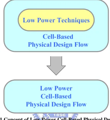
(11) Dynamic techniques allow the dynamic control of certain functional blocks of the design during functional operation. Dynamic techniques involve setting certain functional blocks of the chip into low leakage mode when they are in idle mode. Power switch, or also called sleep transistor, is commonly used to disconnect power supply of functional block when it is in idle mode. This is achieved by connecting a transistor in series with the power supply of the block [5-8]. When the functional block is in idle state, the power switch is turned off; thus reducing the power dissipated by the circuit block. In practice, a network of power switch may be necessary to efficiently control and reduce leakage power dissipation. Another dynamic technique that has been used for leakage power reduction needs dynamically changing the body bias applied to the block [3, 9-10]. During active mode, forward body bias (FBB) is applied to increase the operating frequency. When the block enters idle mode, the forward bias is withdrawn, reducing the leakage. Alternately, reverse body bias (RBB) can be applied during idle mode for further leakage savings. This body bias technique can be combined with a power switch to provide even further leakage power savings; when the block enters idle mode, the supply is collapsed and RBB applied [10]. However, the majority of low power design circuits are implemented with Full-Custom design flow. The Full-Custom designs usually take a lot of time on design and simulation. In order to speed up the design phase and satisfy the demand of Time-to-market, integrating low power techniques into Cell-Based design flow is necessity. At the same time, in order to apply the benefits offered by low leakage techniques into cell-based design, some design issues in physical level must put into consideration. Therefore, the concept of low power cell-based physical design flow is proposed in figure1.1. If the typical EDA tool doesn’t support the placement and routing (P&R) for the design using power switch and body bias, the physical design flow must modify for solving design issues by power switch and body bias. Therefore, some suitable Cell-Based physical design flow for low leakage techniques will be introduction in this thesis. First, in order to provider block-level power optimization, the Voltage Separation technique is introduced. The Voltage Separation partitions design circuit into several groups and routes with individual power grid. In order to avoid coupling noise disturbing the common substrate voltage level, the deep n-well (DNW) is added to diminish noised coupling toward common substrate [11]. Moreover, with a simple contact modification and well pattern insertion, the body bias can be added into 2.
(12) cell-based physical design flow with general standard cell library [12]. Next, a cell layout style with build-in dual supply rail is proposed. By using the cell layout, body bias can be immediately integrated into general cell-based physical design flow. The extra power grid creation and net–to-port connection is also presented. Finally, the power switch which is suitable for cell-based physical design flow is presented.. Figure 1.1 Concept of Low Power Cell-Based Physical Design Flow.. 3.
(13) 1.2 Organization In this thesis, we investigate the feasibility of three low power techniques, Voltage Separation, body bias and power switch, for the cell-based design flow. This thesis presents a set simple but effective low power cell-based design flows via existent commercial EDA tool. In the following chapters, the detailed design process and principle will be presented clearly. In Chapter 2, the relative researches and major efficiency for each low power techniques will be review and presented. In Chapter 3, the details and principle of modified low power cell-based design flow for Voltage Separation, body bias and power switch are presented. All implementations use TSMC 0.18um CMOS technology and Artisan standard cell library support by Taiwan Chip Implementation Center (CIC) [13]. In Chapter 4, the results from these low power techniques are presented that demonstrate the area cost as well as possible design issues. Finally, in Chapter 5, we summary the conclusion and present the future work.. 4.
(14) Chapter 2 Background In Chapter 2, the relative researches and major efficiency for each low power techniques are presented. In Section 2.1, the Voltage Island and Voltage Separation are introduced. Moreover, some considerations for Voltage Separation are also discussed. The basic principle of body bias is introduced in Section 2.2. The effectiveness of reducing leakage current and process variation are presented. Finally, the power switch and MTCMOS are introduced in Section 2.3. The power switch sizing impact on performance is also discussed.. 2.1 Voltage Separation Voltage Island first is proposed by IBM in 2002 [1]. Voltage Island is a system architecture, which can be used to dramatically reduce active and static power consumption for System-on-Chip (SoC) designs. Voltage separation is a sub-step of Voltage Islands and can be accomplished with existent EDA tools. In this thesis, we apply Voltage Separation on a SIMD MAC and treat each one as an individual island. Therefore, the power supply of each island can be managed individually. In Section 2.1, we will briefly explain Voltage Island and Voltage Separation. In previous generations, large functional blocks were not integrated on the same chip, so that voltage level of each block could be made independently. As advance of process technology and increase of chip capability, integrating more functional units into the single chip become a popular design trend. Therefore, traditional approaches to power distribution and performance optimization fail to provide the flexibility of voltage and technology optimization of the previously disintegrated solutions. Figure 2.1 shows a Voltage Island example. Identify minimum voltage level of each element to achieve its required performance. In general, the most performance critical element of the design requires 1.2V supported by the technology in order to maximize it’s performance. Other elements, such as memory or control logic, may 5.
(15) require only 1.0V. Therefore, saving significant active power is available if they can be operated at lower voltages. In addition, voltage flexibility allows pre-designed standard elements to be reused in a new SoC application. Further, some elements, such as analog core, are specified at special voltage, and can be easily accommodated in mixed voltage system. However, some peripheral circuit, such as level converter, may be used for translating voltage level among mixed voltage system. Another type of Voltage Island, shown in Figure 2.2, increase power savings in application more sensitive to standby power, such as battery-powered devices. Method such as clock gating can be used to limit the active power from these idle function units, but the leakage current (or standby) power remains. If the power supplies for these function units are partitioned into islands, the functional units can be completely powered off via switch, eliminating both active and standby components power. There are three islands shown in the figure 2.2. The first island contains the circuitry that listens for the signal to wake up for the rest of system. Using this concept requires that power management be built into the architecture, to handle power sequencing and communication issues. The other two islands contain switches respectively. During the sleep mode, the switch cut off the supply power and both active and standby power can be eliminated. Voltage Separation mentioned in this thesis, like first scenario of Voltage Island in Figure 2.1, can feed each Group with differential voltage supply. The entire design flow for Voltage Separation includes the following steps, as shown below. z Functional partitioning z Synthesis and timing consideration z Floorplanning and Physical design z Logic verification For implementing Voltage Separation, it involves additional step that affects each design phase in the design flow. The following will briefly describe the requirement consideration. z Functional partitioning: The designer should partition the functional units of the design into different islands according to its power characteristic and operation schedule. Example, if component A and component B requires the same voltage level and have the same operation schedule, these two components can be classified to the same island. The islands should be written into individual RTL module when RTL coding, which make grouping islands easily and clearly. z Synthesis and timing consideration: When Synthesis, the effect caused from difference of signal voltage level has to take into consideration. Because of difference voltage level between islands, the level shifter must be added into design. Therefore, the increase of delay from level shifter must take into account when synthesis. 6.
(16) z Floorplanning and Physical design: A Voltage Separation requires complete isolation from each island. In order to enable independent power sequencing. Floorplanning includes determining the number of power sources that meet each island power requirement and how to place the island efficiently [14]. Islands must be floorplanned closely to where the corresponding power pins. z Logic verification: the verification of island functionality is needed. It includes determining the correctness of power management and switching of power control.. Figure 2.1 Timing-critical Voltage Island [1].. Hi-speed Processor 400 MHz 5M gates 10Mbit SRAM 0.9 V SWITCH Sleep Mode. Hibernate. SWITCH. Wake up. Listen Island 50K gates Low Performance 0.7V. Operational Island For Hibernate Mode 500k gates 2Mb SRAM Low performance 0.9V. Figure 2.2 Voltage Island for Power-Sequencing [1]. 7.
(17) Some considerations and issues described above are still not resolved. These are still investigated in the recent literature. In this thesis, we only implement Voltage Separation, which are the sub-step of Voltage Island and accomplished with existent EDA tool. We partition the design into two islands and create its own power grid. In our research, the signal level shifting and other issue are not under consideration. The detailed design flow will be introduced in next chapter.. 2.2 Body Bias Body bias is a dynamic technique that has been used to for leakage power reduction by dynamically changing the body bias applied to the circuit block [Figure2.3]. In general, the forward body bias (FBB) is applied to increases the operating frequency when active mode. When block enter the idle mode, the forward bias is withdrawn, reducing the leakage. In addition, reverse body bias (RBB) can be applied during idle mode for advanced leakage savings. Compare with power switch, the body bias can provide leakage reduction without any performance degradation [3].. Figure 2.3 Outline of body bias. Process parameter variations, which are becoming worse as technology scales, impact the frequency and leakage distribution of microprocessor dies [15]. Due to these die-to-die and within-die variations, some dies can’t achieve the desired frequency target, while others may fail the maximum leakage power specification. Therefore, adaptive body bias has been employed to reduce the impact of these variations and adjust the frequency [16], [17]. The adaptive body bias scheme bases on the frequency of the critical path and use a phase detector which communicates 8.
(18) with a central body bias generator. Therefore, the body bias values which must be applied can be determined by the central body bias generator via embedding measurement. This method, therefore, can ignore any within-die variation. In thesis, the body bias technique is implemented under two design assumption. First, body bias is realized with conventional standard cell library. Because of the Body terminal and Source terminal are tied together, separating these two terminals is need for body bias realization. Therefore, contact of the standard and well pattern will modified for isolation between Body and Source terminal. Besides the remove of contact within the standard cell, the well pattern and metal line which created for body bias signal can be implemented via existent commercial CAD tool. It significantly decreases the design complexity and time. Body bias can also be realized via the dual-supply standard cell. The outlines of the layout will be presented in Chapter 3. The dual-supply standard cells separate the Body and Source terminal embedded in the layout. According to the detailed design, the Body bias techniques can be achieved via existent commercial EDA tool.. 2.3 Power Switch Power switch has first adopted by MTCMOS (Multi-threshold CMOS) technique [18], [19]. MTCMOS is very effective at reducing leakage current in the idle mode. MTCMOS use two types of CMOS: high-VT and low-VT transistor. High-VT devices can be used to reduce leakage currents while low-VT devices can be used whenever high performance is required. MTCMOS technique involves using high-VT transistors to gate power supplies of a low-VT logic block as shown in Figure 2.4. When the high-VT transistors are turned on, the low-VT logic is connected to virtual ground and power, the switching is performed through fast devices. When the circuit enters the idle mode, the high-VT gating transistors are turned off, resulting in a very low leakage current from VCC to ground [20]. MTCMOS circuit can achieve several orders of magnitude reduction in leakage currents through two effects. First, the total effective transistor width of the original CMOS circuit is reduced to the width of the single “off” transistor (provided it is smaller than the original width), and second, the increased threshold voltage results in an exponential reduction in leakage currents [18].. 9.
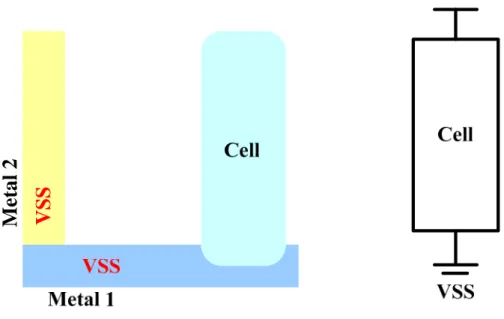
(19) Vcc. Power Switch. Sleep. Low-VT Device. High VT Device. Sleep. Figure 2.4 MTCMOS circuit structure. Power switch (or Sleep transistor) connecting power lines to virtual power lines can be accurately modeled as linear resistors. For a turned-on NMOS transistor sized large enough to ensure performance for requirement, the virtual ground voltage will be close to actual ground. Therefore, the power switch sizing is a key design parameter that affects the performance of circuit. If sized too large, the silicon area would be wasted and switching energy overhead between idle and active modes would be increased. On the other head, if sized too small, then the circuit would be too slow because of increased resistance to ground. Therefore, overdriving and under-driving are used to apply on the power switch [20], [21. Overdriving is used in active mode in order to reduce the frequency penalty of the power switch. Gate under-driving is used in idle mode to further increase the leakage savings by reducing the leakage of the power switch. Besides incurring a little performance penalty, power switch is still a very attractive technique for leakage suppression. In order to insert power switch into Cell-Based design without modifying core design, the appropriate arrangement for power switch is important. Figure 2.5 show the power connection between power grid and standard cell. In our implementation, the power switch is inserted below the power delivery grid between metal-1 and metal-2 [Figure 2.6]. The power switches are distributed throughout the power ring in two columns in order to avoid any current crowding issues. The power switches are designed as large as possible to avoid the sizing impact on performance. 10.
(20) VSS. Metal 2. Figure 2.5 Power connection in general physical design flow.. Cell Power Switch VSS. Metal 2. Cell. Virtual Vss. Virtual VSS VSS. Metal 1 Figure 2.6 Power connection for power switch.. 11.
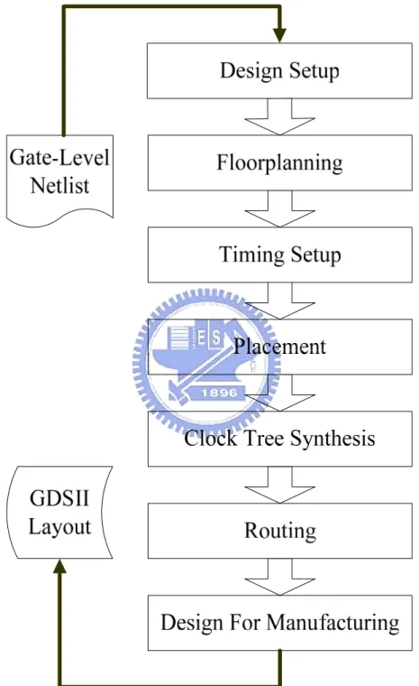
(21) Chapter 3 Implementation In this chapter, each physical design flow is presented. First, general cell-based physical design flow is introduced in Section 3.1. It is divided into seven design phases and purpose of each phase is explained clearly. The physical design flow for Voltage Separation is presented in Section 3.2. In order to avoid substrate noise coupling, deep n-well (DNW) pattern is added for digital circuit core. The body bias for cell-based design flow is shown in Section 3.3. For dual-supply cell, layout of dual-supply cell and connection between port and power net are presented. For general standard cell, the modification of well and contact are introduced. Finally, the power switch implementation is shown in Section 3.4.. 3.1 General Automatic Physical Design Flow The physical design is translating gate-level netlist into a physical representation. Because of the major goal of physical design is standard cells’ placement and routing. The physical design is also called to Auto Place and Routing (APR). The physical design flow includes power/ground line design, partitioning, floorplanning, placement, routing and clock tree synthesis. A general automatic physical design flow is shown in the figure 3.1. From the gate-level netlist to final GDSII file, the entire physical design flow is divided into seven phases. The details of each phase will be described below. First phase in physical design flow is design setup. In this design phase such as technology file, reference libraries, gate-level netlist and power connection are specified. The technology file contains layer definitions and process design rules. It must be specified before creating a design library. The reference libraries are including standard cell library, memory library and IO library. The gate-level netlist is an HDL code after logic synthesis. The EDA tool can load appropriate standard cells from gate-level netlist. Power and Ground port of each standard cell must be associated with corresponding global Power and Ground nets, respectively. 12.
(22) Second phase is floorplanning. In this design phase the core area aspect and Power/Ground Grid will be determined. The core area aspect including standard cell placement direction will be defined by some control parameters. The routing channel and core utilization also be confirm in this design phase respectively. The size of routing channel and core utilization affect the total chip area and probability of routing success. The core power ring and power straps are created to form Power/Ground Grid. The well-defined Power/Ground Grid leads to power arrangement balance and current density. The third design phase is timing setup. In this design phase EDA tool optimize the logic gates, places and routes them to fit in the smallest possible area while meeting all timing constraints by relying on static timing analysis and parasitic extraction estimation and calculation. The forth phase is placement. The placement of standard cells is determined in this design phase. Unsuitable placement of standard cells results in congestion problem which is a limit to the number of nets through the small area. During placement, the congestion problem is fixed by spreading cells apart and wire detour without hurting circuit performance. After placement, the port of each standards cell will connect to Power/Ground Grid. The fifth design phase is clock tree synthesis (CTS). The multi-level buffer trees according to clock specification are added into your target design. The clock skew will be decrease and fit the time specification of your design. The side effort of clock tree synthesis is re-move of some cells and increase of congestion. The EDA tool will optimize the placement of standard cells and fix the congestion problem. The sixth design phase is routing. The goal of routing is drawing Design-RuleCheck-correct (DRC) metal shapes for all interconnect wire while maintaining circuit timing, clock skew, signal net transition and capacitance limits. But this build-in DRC is used for simple verification only, it have to use other tools for sing-off. When routing phase, each metal layer has its own, possibly unique, grid and preferred routing direction. Therefore, every metal line is assign to respective track and is attempting to make long, straight routes. Like placement phase, the congestion problem is expected and resolving with detour routing. The seventh, is also last, design phase is Design for Manufacture (DFM). DFM is used to improve several manufacturability issues and increase manufacturing yield. Such as antenna fixing, metal slotting and metal filler are used to control metal density and prevent from metal liftoff and erosion. The final validation is detailed DRC and Layout Versus Schematic (LVS) verification. The DRC checks physical 13.
(23) formation matching fabrication design constrains. The LVS checks the connectivity of physical layout to its related schematic circuit netlist. Finally, the GDS II file which is free of error can be fabricated in foundry for manufacture.. Figure 3.1 General automatic physical design flow.. 14.
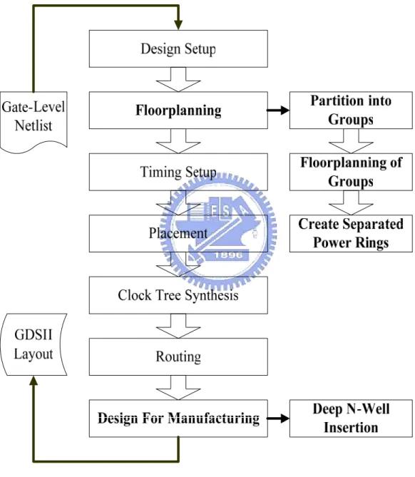
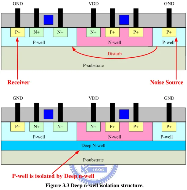
(24) 3.2 Physical Design Flow for Voltage Separation This section presents a design flow for the Voltage Separation. The entire design flow for Voltage Separation is shown in the figure 3.2. Compare with general physical design flow, the difference parts of design phase are design setup, floorplanning and design for manufacturing. The detailed illustrations are shown in remaining of this section. In the floorplanning design phase for Voltage Separation, the extra three steps are added to the design phase. There respectively are z Partition into groups z Floorplanning of groups z Create Separated Power Rings First step is Partition into Groups. According to the demand of system, designer can partition design circuit into several Groups which are supplied to difference voltage level, respectively. Therefore, the power consumption of system can be decrease by providing lowest voltage level for each Group. But at the same time, the core area will be increase result of individual voltage grid and dead space from floorplanning of Groups. In order to increase the design flexibility and decrease the area penalty caused by voltage separation, each Group can adjust island’s aspect and core utilization by some design parameters tuning. After step of Partition into Groups, the Floorplanning of Groups has to implement. According to the pre-plan of power grid, designer can place Group to any region in the core individually. In order to reduce power consumption of system, creating Separated Power Rings surrounding each island respectively is needed. To prevent from fault connection of power rings, the declaration of power rings connection has to specify clearly. In this part, the deep N-well (DNW) can be respectively added to each Group for decreasing substrate noise coupling. The DNW attenuating noise to common substrate is shown in figure 3.3. The DNW isolates the P-well, which is the noise source and P-substrate with each other. The device of characteristic is not affected by DNW impact because DNW implant peak is deep enough, about 2 um. 70dB substrate noise isolation between integrated subsystems is achieved from a circuit level methods [22], substrate noise trapping, descript in figure 3.4. The DNW entirely covering the digital circuit section attenuates the substrate noise passing through the DNW’s walls towards the common substrate (substrate noise trapping). Once into the common substrate, the attenuated substrate noise will proceed towards the DNW protecting the 15.
(25) RF circuit section, making that whole DNW change its electric potential uniformly. Therefore, DNW is needed if there is some sensitivity circuit block on the same die and remarkable noise immunity is achievable. Therefore, if there are two or more than two groups in the design and body bias techniques is applied on NMOS, the coupling noise from two p-well block can be diminished by Double Deep N-well architecture.. Figure 3.2 Physical design flow for voltage separation.. 16.
(26) GND. VDD. P+. N+. N+. GND. N+. P+. P-well. P+. P+. N-well Deep N-well. P-well. Disturb. P-substrate. Receiver. Noise Source. GND. VDD. P+. N+. N+. GND. N+. P+. P-well. P+. P+. N-well. P-well. Deep N-well P-substrate. P-well is isolated by Deep n-well Figure 3.3 Deep n-well isolation structure. VDD. VSS VDD. P+ Nwell. P+. N-well. N+. N+. VSS2 P-well. Nwell. P+. P+. Nwell. P+. N+. N-well. N+. VSS1 P-well. Nwell. Deep N-well. Deep N-well. P-substrate. Substrate Noise Trapping N-well Double N-well Isolation Structure Figure 3.4 Double deep N-well isolation structure.. 17.
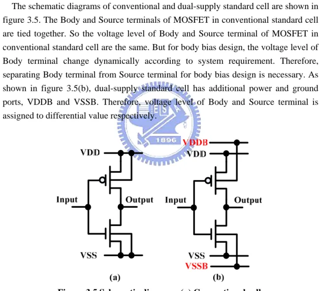
(27) 3.3 Body Bias for Cell-Based Design Flow Two methods of realizing body bias with Cell-Based design flow are introduced in this section. Two methods are individually based on the dual-supply standard cell and modification of well and contact. In Section 3.3.1, the features and extra design phases associated with dual-supply standard cell are introduced. In Section 3.3.2, how to add extra well and strap and remove contact of standard cell are specified.. 3.3.1 Body Bias with Dual-Supply Standard Cell The schematic diagrams of conventional and dual-supply standard cell are shown in figure 3.5. The Body and Source terminals of MOSFET in conventional standard cell are tied together. So the voltage level of Body and Source terminal of MOSFET in conventional standard cell are the same. But for body bias design, the voltage level of Body terminal change dynamically according to system requirement. Therefore, separating Body terminal from Source terminal for body bias design is necessary. As shown in figure 3.5(b), dual-supply standard cell has additional power and ground ports, VDDB and VSSB. Therefore, voltage level of Body and Source terminal is assigned to differential value respectively.. Figure 3.5 Schematic diagrams (a) Conventional cell. (b) Dual-supply cell. The layout of conventional and dual-supply standard cell is shown in figure 3.6. The remarkable variation of those two standard cells is metal lines isolation between Body and Source terminal. Besides isolated metal lines, the remaining part of dual-supply standard cell is almost the same with conventional ones. However, 18.
(28) because of the isolated metal lines have to obey the design rule of layout, the extra gap existed in the standard cell results the increase of cell area. Therefore, the design circuit with dual-supply standard cell has larger area compared with conventional standard cell. The detailed analysis of area penalty will be discussed in Section 4.3.. Figure 3.6 Layout diagrams. (a) General cell. (b) Dual-supply cell. After simply introduces the features of dual-supply standard cell, the entirely physical design flow, shown in figure 3.7, is specified below. In order to fit dual-supply standard cell for conventional physical design flow, there are three additional steps are added into the conventional physical design flow. There are: z Global Net Setting z Create Power Rings z Connect Port to P/G Compare with conventional standard cell, dual-supply ones has extra VDDB and VSSB ports. During expansion the netlist into the design library in Design Setup phase, power and ground ports in standard cells must be associated with corresponding global power and ground net. Using the Global Net Setting, It can specify the global net connections to nets and ports in the standard cells. Because of VDDB (VSSB) is fed another voltage source which differs from VDD (VSS), creating individual power and ground ring in Floorplanning phase is necessary. In the fourth design phase of Placement, standard cells are put into core and connect power and ground ports to corresponding power and ground nets. So power connection between the created power rings and corresponding ports in standard cell is achieving in this step. The remaining design phase is the same with conventional physical ones.. 19.
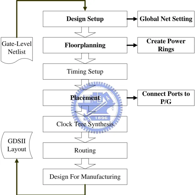
(29) Gate-Level Netlist. Design Setup. Global Net Setting. Floorplanning. Create Power Rings. Timing Setup. Placement. Connect Ports to P/G. Clock Tree Synthesis GDSII Layout. Routing. Design For Manufacturing. Figure 3.7 Physical design flow with dual-supply standard cell.. 20.
(30) 3.3.2 Body Bias with General Standard Cell In the earlier section we introduce how to implement body bias with dual-supply standard cells. But in the general situation, the conventional standard cell is only available in Cell-Based design flow. Therefore, how to add body bias into your design circuit with conventional standard cell is becoming an important topic. In Section 3.3.2, realizing the body bias into design circuit with extra well pattern addition and modification of contact is introduced. With less design step and resource, the body bias can be achieved in cell-based design flow. The example of body bias applied on NMOSFET is illustrated below. The principle of adding body bias for NMOSFET is shown on Figure 3.8. Key point in this design phase is removing body terminal from power grid, adding extra power straps for body terminal voltage controlling and sticking body terminal on power straps. Of course, there are several details must be considered in this design flow. The layout diagram of design process is shown in Figure 3.9. In order to create extra metal liens for VSSB, the standard cells are placed at appropriate intervals, which can be done by using the conventional P&R tool with appropriate parameters. Next, PIMP and DIFF patterns are added to the interval between standard cells. Finally, the removing contact located on VSS line and adding contact on the VSSB line is implemented. The figure 3.10 shows the design flow of body bias with well pattern addition and contact modification. There are five extra steps added into design flow: z Decide Interval z Create Power Ring z Add Straps z Add DIFF & PIMP z Contact Modification During Decide Interval, standard cells are placed at the appropriate interval, which are used to add VSSB metal straps without violating design rule. The appropriate intervals can be determined by design parameters. If biasing both Body terminals of NMOSFET and PMOSFET are needed, it can be realizing, e.g. No Double Back shown in Figure 3.11, by appropriate parameter. When Create Power Ring, just like body bias design flow with dual supply standard cell supported, extra power ring is creating for VSSB strap addition. After creating power rings for VSSB, connecting ports to power and ground nets in the placement design phase is specified. Next, the extra straps for VSSB power line are added from 21.
(31) power delivery grid and inserted into intervals between standard cells. The strap addition can be inserted by conventional P&R EDA tool command. It makes the strap addition more efficiently and avoids error created by hand. Next, the DIFF and PIMP patterns are added by commercial P&R tool command. The patterns overlap to the standard cell can be adjusted by command parameter. According to characteristic of standard cells, this method can adjust the degree of overlap to fit the demand of design. Finally, the modification of contact is implemented. Removing substrate contacts within the standard cells and adding contact on VBBS metal lines make the complete isolation of Body and Source terminals. Therefore, the body bias implementation with modified Cell-Based flow is done. VDD. VDD. VSS. VSS VSSB. VSS. VSS. VDD. VDD. Figure 3.8 Schematic diagram of body bias design principal.. 22.
(32) BODY. PIMP. VSS. SOURCE. VSS. Contact Remove. Interval. Add Contact. VSSB. DIFF. Add Metal. BODY. Figure 3.9 Layout view of body bias design principle.. Figure 3.10 Physical design flow of body bias implementation.. 23.
(33) Bottom of Std Cell VSS Double Back. Std Cell. VDD Std Cell. Interval No Double Back. Std Cell. Std Cell. Figure 3.11 Design parameter of cell placement.. 3.4 Power Switch Implementation In Section 3.4, the implementation of power switch is introduced. Entire design phase of power switch is using Cadence Virtuoso-XL and verified by Mentor Calibre. The NMOSFET power switch implementation diagram is shown in Figure 3.12. The power switches are added below VSS net and distributed throughout the layout in two main VSS columns in order to reduce any current crowding issues.. During implementation of power switch, some layout modification is need for VSS delivery grid. The layout of NMOSFET power switch is indicated in Figure 3.13. The NMOSFET use multi-finger type architecture. The multi-finger architecture provides larger channel width in the limit area, which is suitable for cell-based design and is inserted below the power delivery grid. In order to change general delivery gird to fit power switch insertion, some modification of power delivery is needed. The principle of modification is shown in Figure 3.14 and Figure 3.15. Figure 3.14 and Figure 3.15 show the cross-sections of general VSS delivery grid and modified VSS delivery grid, respectively. Compare Figure 3.14 and Figure 3.15, the contact between metal 1 and metal 2 is removed and a NMOSFET power switch is inserted. The Gate terminal of NMOSFET is driven by sleep signal. Figure 3.16 shows the location of power switches in the entire core. 24.
(34) Cell VSS. Metal 2. Power Switch. Virtual VSS Metal 1 Figure 3.12 Diagram of power switch implementation.. Gate. Drain. Source. Figure 3.13 Layout of multi-finger type NMOSFET power switch.. 25.
(35) Figure 3.14 Profiles of general VSS delivery grid.. VSS. Metal 2. V1 Metal 1 CO Power Switch. N+. Metal 1 CO PO. Metal 1 CO. CO. N+. P+. P-well P-substrate. Figure 3.15 Profile of VSS power delivery grid for power switch. Modified VSS delivery grid, indicating the insertion of power switch and remove of contact.. 26.
(36) Figure 3.16 Entire layout view of power switch implementation.. 27.
(37) Chapter 4 Implementation Results In this chapter, The EDA tools and design environment setup which is used in this thesis is specified in Section 4.1. The area penalty cause by physical design flow for voltage separation is shown in figure 4.2. The body bias design requirement method and implementation consideration is described in Section 4.3. In Section 4.4, the extra area and routing resource for power switch is introduced. Finally, the advantages and drawbacks are discussed in Section 4.5.. 4.1 Implementation Environment Setup During entire research process, TSMC 0.18um CMOS Mixed-Signal 1P6M process and Artisan standard cell library is adopted. The benchmark circuit for proposed design flow is a Single-Instruction-Multiple-Data Multiply and Accumulate Unit (SIMD MAC). The Hardware Description Language (HDL) for behavioral coding is Cadence Verilog-XL. The EDA tool for logic synthesis is Synopsys Design Vision. The circuit verification and debug tool is Spring Soft Debussy. The APR for physical design is Synopsys Astro. The tool for physical verification is Cadence Virtuoso-XL and Mentor Calibre. The SIMD MAC architecture is shown in figure 4.1. The recursive architecture is chosen to implement SIMD MAC. The recursive architecture involves building wider vector elements out of several of the narrower vector elements and adding the multiple results together. The execution results can be determined iteratively by repeating the data back through the unit over more than one cycle. Radix-4 modified booth encoding and Wallace tree are used to speed up the accumulation. The hot one coding compensates the two’s complement increment bits of each partial product created from booth encoding. Table 1 shows the summary of input and output ports. The width of input and output are 32 and 40, respectively. The wider width of output originates from the iterative accumulative execution and prevents results from saturation easily. The Tag file in Table 1 decides the accumulative data from 28.
(38) accumulator within the SIMD MAC or loading from external accumulators. Table 2 introduces the operation of each SIMD instruction. The multiply with implicit accumulate (MIA) features are also added in this SIMD MAC.. Multiplier Y[31:0]. Sign Extension & Mux. Vector Mask & Booth Encoder. Multiplicand X[31:0]. Booth Decoder. Hot One Coding. Shifter & Mux. Mux. Wallace Tree CSA + CLA. Accumulate Z[31:0]. Output [39:0] Figure 4.1 SIMD MAC architecture. Table 1 SIMD MAC input & output summary Title. Description. Notes. Ac. 32-bits Accumulator. ---. Rm. 32-bits Multiplier. ---. Rs. 32-bits Multiplicand. ---. Tag. Select Accumulator. ---. OP. 4-bits operation code. Six instruction are defined below: 0’b0000 = MIA 0’b1000 = MIAPH 0’b1100 = MIABB 0’b1101 = MIABT 0’b1110 = MIATB 0’b1111 = MIATT. Out. 40-bits output. ---. 29.
(39) Table 2 SIMD MAC instruction specification.. Instruction. MIA. Results Latency (Throughput). Instruction Description. 2. Ac=Rm* Rs+Ac. MIAPH. 2. Ac=Rm[b]*Rs[b]+ Rm[t]*Rs[t]+ Ac. MIAxy. 1. Ac= Rm[x]* Rs[y]+ Ac. Note : x, y can top-half[31:16] or bottom-half[15:0] operand. 4.2 Physical Design Flow for Voltage Separation The use of voltage separation permits operating different groups of the design at different voltage level in order to optimize the overall chip power consumption. Moreover, the groups can even close the voltage supply when they are in the idle situation. But the voltage separation definitely makes the design process even more complicated with respect to static timing, power routing, floorplanning, etc. The Figure 4.2 shows an example problem associated with voltage separation. The cells belongs to each island are only placed to area indicating in the figure. The limited placed area restricts the flexibility of cell moving space, which may be used to resolve the timing requirement and wiring congestion. The larger core area results in the waste to area utilization and small one makes the trouble of wiring congestion. Therefore, how to decide the appropriated size of core area and how to place each group to appropriate location is an important issue for voltage separation.. 30.
(40) Core Area. Limited Place Range Figure 4.2 Example of limited placed area, the cells belongs to each group are placed to indicating area. A design using Voltage Separation needs to put together the groups which are powered by the same voltage source. Besides, the groups need to be placed close to the power pads in order to minimize the power routing complexity and the IR drop. Since each group requires its own power grid, the overhead with respect to area and delay is unavoidable. It may have additional area overhand due to potential dead spaces if two or more power rings can not packed perfectly. Figure 4.3 shows the dead space is caused by each power ring packed imperfectly. Because each group has its own power grid, each power gird can adjust the width of metal line to fit the design demand. Therefore, the area overhead is not a critical issue if the power ring packed perfectly. Figure 4.4 shows a layout diagram. There are four SIMD MACs which everyone has its own power rings. The area overhead created by voltage separation is shown in Table 4. There is only about 1 % area overhead in voltage separation.. 31.
(41) Figure 4.3 Example of dead space, the dead space is caused by the each power rings packed imperfectly.. Figure 4.4 Example of voltage separation. Each group has its own power rings.. 32.
(42) Table 3 Area overhead of voltage separation Type. Area. Normalized Area. SEPARATED POWER RINGS. 1.375X1.179. 1. UNSEPARATED POWER RINGS. 1.390X1.179. 1.011. 4.3 Body Bias for Cell-Based Design Flow In Section 4.3.1, the implementation result using dual-supply cell is discussed. Because dual-supply cell separates the body and source terminal, extra gap and layout design rule will result in increasing of cell height. In Section 4.3.2, the body bias implementation with conventional cell has to leave appropriate interval for straps insertion. The interval will incurs core area overhead. The detail estimation is discussed in this section.. 4.3.1 Body Bias with Dual-Supply Standard Cell In this section, the dual-supply standard cell library is proposed for body bias within cell-based design flow. Figure 4.5 shows the outlines of general and dual-supply standard cell. The general standard cell is provided by Artisan for TSMC 0.18um process. The cell height of general standard cell is 5.84um. Power and ground rails are designed to be 0.8um respectively. When dual-supply standard cell is adopted for body, one rail is powered from VDD (VSS), and another rail is powered from VDDB (VSSB) for body bias. Because each rail of dual-supply cell sinks less current than rail of the general cell that is powered from single VDD (VSS). Thus, the width of power rails can be shrunk. Meanwhile, VDDB of the dual-supply standard cell is further scaled to 0.3um because current magnitude of Body terminal is less than Source terminal. The cell height of dual-supply standard cell is then changed to 6.3 um, which accounts to 7.9% area overhand compared to general cell. For the body bias implementation with dual-supply standard cell, the advantage is routing can be directly performed after placement. The existed APR tool can be used to automate the placement and routing of the cell most efficiently. Figure 4.6 shows the architecture of power rail connection. In Figure 4.6, there are four power rings, which create for each power rail connection.. 33.
(43) VDDB 0.3 um VDD 0.8 um. VDD 0.5 um. 5.84 um. 6.3 um. VSS 0.5 um. VSS 0.8 um. VSSB 0.3 um (a). (b). Figure 4.5 Outline of cells. (a) General cell. (b) Dual-supply cell.. VSSB VDDB VSS VDD Core Area. Dual-Supply Cell. Figure 4.6 Power rail connection architecture.. 34.
(44) 4.3.2 Body Bias with General Standard Cell This section introduces the body bias implantation with general standard cell. In order to add straps between standard cells, an interval is left for strap and well pattern insertion. Figure 4.7 shows the outline of cell placement. The cell placement of general design flow is shown in Figure 4.7 (a). The cells are placed side by side and shared VSS and VDD power rails with other cells. This type of cell placement can increase use efficiency of core area. Figure 4.7 (b) shows the cell placement for body bias. When cells are placed, an appropriate interval is left between cells for realizing body bias. The width of interval can be controlled by design parameter “Row/Core Ratio”. Therefore, the area overhead depends on how large the interval area occupy in the entire core size. Table 4 show the area overhead created by body bias with general cell. According to SIMD MAC experiment result, the core area is increased from 692 um x 692um to 750 um x 750 um. It accounts to 17% area overhead compared with SIMD MAC without body bias. The layout diagram for body bias with general cell is show in Figure 4.8. The white block indicating in the figure show some straps are inserted into the intervals betweens cells. The extra power rings supply VSSB power line for body bias.. Bottom of Std Cell VSS. Std Cell. VDD. Std Cell. Std Cell Std Cell. Interval Std Cell Std Cell Std Cell Std Cell (a). (b). Figure 4.7 Cell placement. (a) Cell placement for general design flow. (b) Cell placement for body bias, the straps and well are added within the interval.. 35.
(45) Table 4 Area Overhead for body bias with general cell Interval Space. Area. Normalized Area. SIMD MAC (without body bias). 0. 692 um x 692 um. 1. SIMD MAC (with body bias). 2 um. 750 um x 750 um. 1.174. Figure 4.8 Layout diagram for body bias with general cell.. 36.
(46) 4.4 Power Switch Implementation During cell-based design flow, the APR tool determines the major part of cell placement and power gird architecture. Figure 4.9 show the outline of cell placement and power grid architecture. The cells are placed within the core area by timing analysis. Two power rings, VSS and VDD, are around the core area and deliver power to the cell equally. If designer want to add power switch into the design circuit, the architecture of power grid have to be consideration. The carefully implementation of power switch usually can decrease the area overhead without complicated modification. In our research, the NMOSFET power switch is added into the SIMD MAC. The concept of adding power switch into cell-based design flow is shown in Figure 4.10. The power switches are inserted into the power delivery grid between the metal-1 and metal-2. The power switch switches are distributed through the layout in two columns in order to reduce any current crowding issues in the power delivery grid. At the same time, the power switched addition, like described in Section 3.4, is not implemented by APR tool. So the cut-off signal routing which drives the gate of the switches has to realize by designer. Because the power switches are placed below the power grid, the area overhead created by power switches is nearly 0%. The layout diagram of power switches placement is shown in the Figure 4.11.. VSS VDD Core Area. Standard Cell. Figure 4.9 Cell placement and power grid architecture for cell-base design flow. 37.
(47) Cell VSS. Metal 2. Power Switch. Virtual VSS Metal 1 Figure 4.10 Concept of adding power switch into cell-based design circuitry.. Figure 4.11 Power switches placement.. 38.
(48) 4.5 Summary In this section, the features of low power techniques are summarized. Table 5 shows the summary of the low power techniques introduced in this thesis. Because of dual-supply standard cell is not available in our research; the area overhead of dual-supply cell indicates the star mark and the meaning of the number represent the increase percentage per cell compare with general cell. Beside the method using dual-supply cell for body bias, other design methods need extra pattern to realized techniques. The semi-automation represents that some design phases are realized by designer, not EDA tool. All techniques introduced in our research, e.g. voltage separation, body bias and power switch, are realized and implemented on SIMD MAC. Actually, all techniques introduced in this thesis can realize on every design circuit which adopts cell-based design flow. Figure 4.12 shows a layout diagram of streaming clusters with voltage separation technique. Streaming architecture has been suggested as an efficient architecture for both media applications and baseband architecture for software defined radios. Table 5 Summary of low power techniques Technique type. Area overhead. Extra pattern. Implementation style. Voltage Separation. 1.1%. DNW. Semi-automation. Dual-supply cell. *7.9%. none. Fully-automation. General cell. 17 %. Contact / DIFF. Semi-automation. --. none. Semi-automation. Body Bias. Power Switch. * The cell height of dual-supply accounts to 7.9% area overhand compared to general cell.. 39.
(49) Power Ring. Power Ring Power Ring. Cluster 1. Power Ring. Cluster 3. Cluster 2. Power Ring. Memory. Cluster 4. Figure 4.12 Layout diagram of streaming cluster with voltage separation. Each cluster has its own power ring.. 40.
(50) Chapter 5 Conclusion and Future Work 5.1 Conclusion As the power consumption of VLSI design increases from one generation to the next, it is becoming more important to control power dissipation even when circuit in idle mode. To meet the power requirement of advanced VLSI design, several simple yet effective physical design flows using existent commercial EDA tool have been presented. By using Voltage Separation techniques, the design circuit can be partitioned into several islands and providing minimum voltage for reducing power is possible. At the same time, the deep n-well (DNW) is added to diminish noised coupling towards common substrate. Moreover, a cell layout style with build-in dual supply rail is proposed. By using the cell layout type, body bias can be immediately embedded in typical cell-based design flow. The extra power grid creation and port connection is also presented. By using conventional cell library, the body bias also can be added into cell-based design flow via a simple contact modification and well pattern insertion. Finally, the power switch which is suitable for cell-based design flow is shown. By the careful design, the power switches are inserted between metal-1 and metal-2 layer and suffer less area overhead. By embedding low power techniques into physical design flow. A design circuit with low power technique feature is available. Therefore, this thesis provides an opportunity to realize several low power techniques relied on cell-based method. Although some simple low power techniques are realized, several enhancements, such as partition islands, sizing of power switch and physical design considerations, are still needed for the EDA tool. Further, creating an industry-wide design flow with robust capability is essential. These include functional partitioning, synthesis, timing analysis, power analysis, test, simulation and physical design.. 41.
(51) 5.2 Future Work Although several low power techniques have been added into the cell-based design flow, a comprehensive power management unit is still essential for a real SoC system. This power management unit not only deals with performance coherence between functional blocks as well as handles power sequencing and communication issues, but also determines the minimum voltage level for each functional block or provides optimized voltage for body bias immediately. This information may be different according to using process technology such as low power process or high speed process. Further, some side effect, e.g. leakage current of NMOS increases dramatically in small channel width, will probably damage the effectiveness of the low power techniques in 0.13nm generation or beyond. Therefore, a robust block-level simulation for leakage efficiency in needed.. 42.
(52) Bibliography [1]. [2]. [3]. [4]. [5]. [6]. [7]. [8]. [9]. [10]. [11]. [12]. [13] [14]. D. E. Lackey, P. S. Zuchowski, T. R. Bednar, D. W. Stout, S. W. Gould, and J.M. Cohn, “Managing power and performance for system-on-chip designs using voltage islands,” IEEE/ACM International Conference on Computer Aided Design, ICCAD 2002, pp. 195-202, 10-14 November, 2002. T. Kam, S. Rawat, D. Kirkpatrick, R. Roy, G. S. Spirakis, N. Sherwani, and C.Peterson, “EDA challenges facing future microprocessor design,” IEEE Transactions on Computer Aided Design, vol. 19, pp. 1498-1506, Dec. 2000. J. W. Tschanz, S. G. Narendra, Y. Ye, B. A. Bloechel, S. Borkar, and V. De, “Dynamic sleep transistor and body bias for active leakage power control of microprocessors,” IEEE Journal of Solid-State Circuits, vol.38, no. 11, pg. 1838-1845, November 2003. J. Tschanz, Y. Ye, L. Wei, V. Govindarajulu, N. Borkar, S. Burns, T. Karnik, S. Borkar, and V. De, “Design optimizations of a high performance microprocessor using combinations of dual-Vt allocation and transistor sizing,” in Symp. VLSI Circuits Dig. Tech. Papers, 2002, pp. 218–219. T. Kuroda, T. Fujita, S. Mita, T. Nagamatsu, S. Yoshioka, K. Suzuki, F. Sano, M. Norishima, M. Murota, M. Kako, M. Kinugawa, M. Kakumu, and T. Sakurai, “A 0.9-V, 150-MHz, 10-mW, 4mm , 2-D discrete cosine transform core processor with variable threshold-voltage (VT) scheme,” IEEE Journal of Solid-State Circuits, vol. 31, pp. 1770-1779, Nov. 1996. Calhoun, B., F. Honore, A. P. Chandrakasan, "A Leakage Reduction Methodology for Distributed MTCMOS," IEEE Journal of Solid-State Circuits, pp. 818-826, May 2004. V. Kursun and E. G. Friedman, " Sleep Switch Dual Threshold Voltage Domino Logic with Reduced Standby Leakage Current," IEEE Transactions on Very Large Scale Integration (VLSI) Systems, Vol. 12, No. 5, pp. 485-496, May 2004. Kao, J., A. P. Chandrakasan, "Dual-Threshold Techniques for Low-Power Digital Circuits," IEEE Journal of Solid-State Circuits, pp. 1009-1018, July 2000. S. Thompson, I. Young, J. Greason, and M. Bohr, “Dual threshold voltages and substrate bias: keys to high performance, low-power, 0.1-m logic designs,” in Symp. VLSI Technology Dig. Tech. Papers, 1997, pp. 69-70. S. Narendra, A. Keshavarzi, B. A. Bloechel, S. Borkar, and Vivek De, “Forward Body Bias for Microprocessors in 130-nm Technology Generation and Beyond,” IEEE Journal of Solid-State Circuits, vol. 38, pp. 696-701, May 2003. L. T. Clark, E. J. Hoffman, J. Miller,M. Biyani, Y. Liao, S. Strazdus, M. Morrow, K. E. Velarde, and M. A. Yarch, “An embedded 32b microprocessor core for low-power and high-performance applications,” IEEE J. Solid-State Circuits, vol. 36, pp. 1599-1608, Nov. 2001. W. K. Yeh, S. M. Chen, Y. K. Fang (2004) “ Substrate Noise-Coupling Characterization and Efficient Suppression in CMOS Technology", IEEE T-Electron Device, Vol. 51, No.5, pp.817-827 http://www.cic.org.tw J. Hu, Y. Shin, N. Dhanwada and R. Marculescu, “Architecting Voltage Islands in Core-based System-on-a-Chip Designs,” in Proc. ISLPED, oo.180-185, Aug. 2004. 43.
(53) [15] K. A. Bowman, S. G. Duvall, and J. D. Meindl, “Impact of die-to-die and within-die parameter fluctuations on the maximum clock frequency distribution,” in IEEE ISSCC Dig. Tech. Papers, Feb. 2001, pp. 278-279. [16] J. Tschanz, J. Kao, S. Narendra, R. Nair, D. Antoniadis, A. Chandrakasan, and V. De, “Adaptive body bias for reducing impacts of die-to-die and within-die parameter variations on microprocessor frequency and leakage,” IEEE Int. Solid-State Circuits Conf. Dig. Tech. Papers, 2002, pp. 422-423. [17] J. Tschanz et. al., "Effectiveness of adaptive supply voltage and body bias for reducing impact of parameter variations in low power and high performance microprocessors," IEEE Journal of Solid-State Circuits, pp. 826-829, May 2003. [18] Kao, J., A. P. Chandrakasan, "Dual-Threshold Techniques for Low-Power Digital Circuits," IEEE Journal of Solid-State Circuits, pp. 1009-1018, July 2000. [19] Calhoun, B., F. Honore, A. P. Chandrakasan, "A Leakage Reduction Methodology for Distributed MTCMOS," IEEE Journal of Solid-State Circuits, pp. 818-826, May 2004. [20] S. Mutoh, T. Douseki, Y. Matsuya, T. Aoki, S. Shigematsu, and J. Yamada, “1-V Power Supply High-Speed Digital Circuit Technology with Multithreshold-Voltage CMOS,” IEEE Journal of Solid-State Circuits, pp. 847-854, August 1995. [21] H. Kawaguchi, K. Nose, and T. Sakurai, “A CMOS scheme for 0.5 V supply voltage with pico-ampere standby current,” IEEE Int. Solid- State Circuits Conf. Dig. Tech. Papers, Feb. 1998, pp. 192-193. [22] L. M. Franca-Neto, P. Party, M. P. Ly, R. Rangel, S. Suthar, T. Syed, B. Bloechel, S. Lee, C. Burnett, D. Cho, D. Kau, A. Fazio and K. Soumyanath, “Enabling High-Performance Mixed-Signal System-on-a-Chip (SoC) in High Performance Logic CMOS Technology,” IEEE VLSI Circuit Symposium, June, 2002. 44.
(54)
數據
![Figure 2.2 Voltage Island for Power-Sequencing [1].](https://thumb-ap.123doks.com/thumbv2/9libinfo/8502499.185333/16.892.153.755.737.1110/figure-voltage-island-for-power-sequencing.webp)

+7

相關文件
American Association of School Librarians, Association for Educational Communications and Technology.. Information power: Building partnerships
Lecture 16: Three Learning Principles Occam’s Razor?. Sampling Bias Data Snooping Power
In this chapter, a dynamic voltage communication scheduling technique (DVC) is proposed to provide efficient schedules and better power consumption for GEN_BLOCK
為主要的積體電路單元元件,此元件同時利用電子與電洞兩種載子,來進行電流的傳
“Reliability-Constrained Area Optimization of VLSI Power/Ground Network Via Sequence of Linear Programming “, Design Automation Conference, pp.156 161, 1999. Shi, “Fast
A segmented current steering architecture is used with optimized performance for speed, resolution, power consumption and area with TSMC 0.18μm process.. The DAC can be operated up
Alonso, “Electronic ballast for HID lamps with high frequency square waveform to avoid acoustic resonances,” 2001 IEEE Sixteenth Annual Conference Record of the Applied
“ Electronic ballast for HID lamps with high frequency square waveform to avoid acoustic resonances, ” 2001 IEEE Sixteenth Annual Conference Record of the Applied Power Electronics
