As device geometry is scaled down to deep submicrometer re-gion, the parasitic capacitance between closely spaced metal lines becomes important in the issue of resistance-capacitance time de-lay.1Meanwhile, high stress in the intermetal dielectric (IMD) film also degrades the reliability of interconnects.2,3Especially the prob-lem becomes more serious if the deposition temperature of IMD is high.3Therefore, for scaling down devices, a novel IMD with low dielectric constant, low stress, and low deposition temperature is essential. The fluorinated oxide film prepared by conventional liquid phase deposition (C-LPD) with adding boric acid or water as a supersaturation initiator was verified to meet the requirements.4-8
For the C-LPD film, the fluorine concentration has been shown to increase with the decreasing quantity of supersaturation initiator.9 Therefore, the quantity of supersaturation initiator should be reduced for increasing the fluorine concentration and reducing the dielectric constant. However, the deposition rate, which decreases as the quan-tity of initiator decreases, become a limiting factor while increasing the fluorine concentration.10The fluorine concentration of C-LPD film at most achieves 6.25 atom %.9
Sakai et al. first proposed the notion of controlling the degree of supersaturation for the deposition solution by changing the deposi-tion temperature from the soludeposi-tion-preparadeposi-tion temperature, instead of adding any supersaturation initiator.11Kawahara et al. studied the chemical composition, the p-etch rate and the stress for this kind of oxide films prepared by using 2-3 M H2SiF6.12According to their results, a higher H2SiF6concentration, i.e., 3 M, led to a higher film density and a higher fluorine concentration. In this work, using a nondiluted (4 M) H2SiF6 solution and the temperature difference technique proposed by Sakai et al., the LPD method is expected promising in preparing highly fluorinated film. This method is termed temperature difference-based LPD (TD-LPD).
Oxide films with high fluorine concentrations are generally hygroscopic, i.e., the film properties easily change after moisture stress and/or thermal annealing.5,6To apply the TD-LPD film as an IMD, the reliability issues must be clarified in advance. Since an IMD may be thermally treated and exposed to moist ambient more than once, the reliability of the film is thus studied through evaluat-ing physicochemical and electrical properties durevaluat-ing the test of repeated annealing (4008C) and boiling (in 1008C water). A feasible mechanism that accounts for the variation of the properties during the test is proposed. High temperature (>4008C) stability of the film is also evaluated.
Experimental
Preparation of TD-LPD film.—Silica powder was added to a 4 M
H2SiF6solution and then dissolved by stirring at ,08C for 24 h. After removing the undissolved silica by filtering, the saturated solu-tion was heated to 258C, and became supersaturated. After cleaning, the wafers were immersed in the solution and, then, the TD-LPD film was gradually deposited on the wafers. Thus, the difference between the solution preparation temperature and the deposition temperatures was 258C.
Reliability test.—Reliability of the TD-LPD film was evaluated
by using (i) repeatedly annealing and boiling test (RABT), and (ii) high temperature (400-8008C) annealing in N2for 30 min. Figure 1 is the RABT flow diagram with denotation of films at different stages. The film before any treatment is denoted as the as-deposited film. The as-deposited film processed with the first annealing at
Reliability of Fluorinated Silicon Oxide Film Prepared by Temperature
Difference-Based Liquid Phase Deposition
Ching-Fa Yeh,
zYueh-Chuan Lee,* and Su-Chen Lee
Department of Electronics Engineering and Institute of Electronics, National Chiao Tung University, Hsinchu, Taiwan
Fluorinated silicon oxide film prepared by using temperature difference-based liquid phase deposition is very potential for use as an intermetal dielectric owing to its high fluorine concentration (8.6 atom %), low dielectric constant (3.46), low stress (41 MPa), low leakage current density (4.6 3 1029A/cm2at 2 MV/cm), and low deposition temperature (room temperature). In this work,
we closely examine reliability issues including resistance to water absorption and thermal stability by adopting the repeatedly annealing (4008C) and boiling test. After the test, the net increase in the dielectric constant is only 0.02; the stress changes within 224 to 41 MPa with a resultant zero stress; the leakage current density increases slightly to 8.0 3 1029A/cm2. Obviously the film
will preserve its attractive properties in a back-end process similar to the test. Accompanied with the investigation of p-etch rate, thermal desorption spectroscopy, and Fourier transform infrared spectroscopy, a feasible mechanism that accounts for the variation of the properties during the test is proposed. A high temperature (>4008C) annealing effect is also studied. The film is thermally stable up to 6008C, which is limited by the decomposition of Si–F bonds. The thermal stability of 6008C is obviously sufficient for intermetal dielectric application.
© 2000 The Electrochemical Society. S0013-4651(99)12-019-6. All rights reserved. Manuscript received December 6, 1999.
* Electrochemical Society Student Member. z E-mail: [email protected]
4008C for 30 min in N2is denoted as the first annealed film; while the as-deposited film processed with first annealing and first boiling stress in 1008C water for 1 h is denoted as the first boiled film. The second annealed and the second boiled films also denote the films after second annealing and second boiling, respectively.
Measurements.—The dielectric constant (1 MHz) was
deter-mined by C-V measurement through the metal oxide semiconductor (MOS) capacitor structure (A1/110) nm oxide/p-Si). The stress of
,260 nm thick film was calculated from measured curvature based
on Stoney’s equation using a Tencor FLX-2320 instrument. The characteristic of current density vs. electrical field (J-E) was meas-ured using HP4145B system also with the MOS capacitor, where the Al electrode was negatively biased. Etch rate of the film using p-etch solution (HF:HNO3:H2O 5 3:2:60) was employed to investigate the film density. The desorbed species, including H2O and HF during heating, were monitored by using thermal desorption spectroscopy (TDS). The content of the Si–F bond was evaluated by Fourier trans-form infrared spectroscopy (FTIR).
Results and Discussion
As listed in Table I, fluorine concentration, dielectric constant, stress, and leakage current density (2 MV/cm) of as-deposited TD-LPD film are 8.6 atom %, 3.46, 41 MPa, and 4.6 3 1029A/cm2, respectively. Properties of films prepared at room temperature by C-LPD,7-9,13 electron cyclotron resonance chemical vapor deposi-tion (ECR-CVD)14,15and room temperature chemical vapor deposi-tion (RT-CVD)5,16are also listed in Table I for comparison, where C-LPD films are prepared by using water as the supersaturation initia-tor. Compared with C-LPD film, TD-LPD film exhibits higher fluo-rine concentration, lower dielectric constant, lower stress, and com-parable leakage current level. Compared with ECR-CVD and RT-CVD films, TD-LPD film demonstrates much better insulating prop-erty in terms of two orders of magnitude lower leakage current den-sity. TD-LPD film seems very potential for IMD application in terms of its attractive properties.
Figure 2 shows the dielectric constant of the film during RABT. The dielectric constant changes in the range of 3.33-3.48. After the test, the dielectric constant increases only by 0.02. This result reveals that the film can well preserve the merit of low dielectric constant in a back-end process similar to the test.
During the first annealing and boiling cycle, the dielectric con-stant first decreases from 3.46 to 3.33, then it increases back to 3.46, implying that some polar H2O species in the film are first removed and then refilled. In fact, H2O species in a fluorinated oxide film have been recognized as absorbed molecular H2O in the pore struc-ture, hydrogen-bonded H2O to Si–OH, and H2O associated Si–OH bonds, where the former two H2O species can be removed by 4008C annealing.17,18 Therefore, desorption/absorption of the two H
2O species accounts for the variation in the dielectric constant in the first cycle. In addition, the Si–OH bond density after the first boiling is not expected to be increased, because the dielectric constant of the first boiled film is not higher than that of the as-deposited film. How-ever, the dielectric constant of the second annealed film becomes higher than that of the first annealed film. This result implies that additional Si–OH bonds, which are thermally stable beyond 4008C, are generated during the second annealing.
In addition to the annealing effect, the first annealed and the sec-ond annealed films also differ with respect to variation in the tric constant after the subsequent boiling. The increase in the dielec-tric constant after the second boiling (Dk2) is smaller than that after the first boiling (Dk1). This fact indicates that resistance to H2O absorption for the second annealed film is better than that for the first annealed film. Obviously, the dielectric constant tends to vary less in the latter annealing and boiling cycle. However, the mechanism that the second annealed film has an improved resistance to H2O absorp-tion is still not clear.
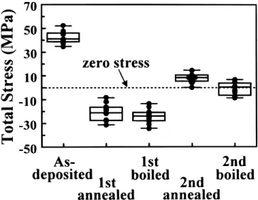
The stress, which is also referred to as the total stress, is also stud-ied. According to Fig. 3, during the test, the total stress varies within
224 to 41 MPa; after the test is becomes nearly zero, i.e., free of
stress. This finding reveals that for TD-LPD film, the low stress merit can obviously be preserved after annealing and boiling cycles. In fact, the total stress is the sum of thermal stress and intrinsic stress. For the as-deposited film, the thermal stress is zero since the film is deposited at room temperature. After first annealing, the change in stress is 263 MPa, which is close to the calculated thermal stress (278 MPa at 4008C).8Therefore, the variation in the stress after the first annealing is mainly attributed to the thermal stress induced dur-ing the annealdur-ing process. The stress remains almost unchanged after (the first or second) boiling. Notably, the stress increases by about 32 MPa after the second annealing. Since Si–OH bonds may be gener-ated during the second annealing, the increased (tensile) stress is pre-sumably due to the formation of additional Si–O–Si bonds between Si–OH bonds. Meanwhile, the film must also be densified with the increasing S–O–Si bond density. These references are examined using a p-etch rate test and TDS.
The p-etch rate for the second annealed film is 12.3 Å/s, which is lower than 13.5 Å/s for the first annealed film by 8.9%, indicating that the second annealed film is more densified. Because the second annealed film is annealed in 4008C ambient for totally 1 h (first annealing 1 second annealing), one may suspect that longer anneal-Table I. Properties of films prepared at room temperature by TD-LPD, C-LPD, ECR-CVD, and RT-CVD.
TD-LPD C-LPD ECR-CVD RT-CVD
F concentration 8.6 atom % 1.86-6.25 atom % 8.55%a 5.3 3 1021atom/cm3
Dielectric constant 13.46 13.52,4.2311 123.17 13.7
Stress (MPa) 4111. 11.83,10711. 274.21 501.
Current density at 4.6 3 1029 2 3 1029to 6 3 1028 ,2 3 1026 ,4 3 1027 2 MV/cm (A/cm2)
aRatio of FTIR peak intensity (Si–F/Si–O).
ing time makes the film more dense. The p-etch rate for the first annealed film with further 30 min annealing (without and boiling) is thus investigated and found to be 13.6 Å/s, which is close to that for the first annealed film. This further annealing cannot make the first annealed film more dense. Therefore, the H2O molecules absorbed by the film during the first boiling must play an important role in enhancing the generation of the additional Si–OH bonds, and the subsequent densification of film.
Figure 4a shows the J-E curves for, in an increasing order of cur-rent density, as-deposited, second annealed, second boiled, first boil-ed, and first annealed films. The breakdown fields for various films are within 6.4-7.7 MV/cm, much higher than the operation field applied to an IMD. Figure 4b shows the distributions of current den-sity at 2 MV/cm for various films. The medium current denden-sity (J50) for the as-deposited film is 4.6 3 1029A/cm2. After the first anneal-ing, the J50increases by a factor of 5 to 2.3 3 1028A/cm2. The in-crease in J50may be attributed to decomposition of weak S–F bonds and/or Si–OH bonds during first annealing with the generation of dan-gling bonds, which are electrically active traps.15,19 After the first boiling, the J50decreases to 1.2 3 1028A/cm2, implying that a part of dangling bonds is passivated by water or related species.19-21After the second annealing, the J50further decreases to 7.0 3 1029A/cm2. This decrease in J50is attributable to that the film becomes densified. The densified film is very stable in electrical insulating property in terms of scant variation in J50after further (second) boiling.
So far, we have inferred that the film becomes densified after the second annealing, in terms of increased stress, reduced p-etch rate and stabilized insulating property. However, the densification pro-cess has not been well understood. Therefore, we use TDS to inves-tigate the process. As mentioned previously, there are three H2O species in a fluorinated oxide film. HF may also desorb accompany-ing the desorption of H2O.18We thus monitored desorbed species of H2O and HF. A heating recipe for TDS measurements is designed so that the heating temperature increases from ,40 to 4008C at a speed of 408C/min, and maintains at 4008C for 30 min, then increases to
,8008C at the same rate. The holding of temperature at 4008C for
30 min is to simulate the first or the second annealing of RABT. The heating at >4008C is to monitor Si–OH bonds.
Figure 5 shows the TDS spectra for the as-deposited film. Obvi-ously, there are three H2O (m/e5 18) peaks and three HF (m/e 5 20) peaks in the spectra. Each of the three HF peaks appears to cor-respond to one H2O peak. In addition, we also find that (i) the inten-sity of every HF peak is weaker than that of the corresponding H2O peak, and (ii) the evolution of every HF peak lags behind that of the corresponding H2O peak. We therefore inferred that the H2O mole-cules react with Si–F bonds in the film during heating, and drives HF desorption together with generation of Si–OH bonds. In fact, the first
HF peak (at ,2488C), which is driven by the most intense water de-sorption (H2O in the pore structure), is the most faint, revealing that a higher temperature is required to generate Si–OH bonds. This find-ing accounts for that the Si–OH bond density in the film is not in-creased by 1008C boiling treatment. When the film is annealed below 4008C, the generation of Si–OH bonds is mainly driven by hydrogen-bonded H2O. The hydrogen bond between H2O and Si–OH breaks early from ,2908C, as expressed in Eq. 1
Si–OH?????????H2O r Si–OH??//??H2O F [1] Hydrogen bond Broken
The desorbed H2O molecules in Reaction 1 can react later with Si–F bonds, leading to formation of Si–OH bonds and desorption of HF from ,3208C. This is hydrolysis of Si–F bonds, as expressed in Eq. 2
Si–F 1 H2O r Si–OH 1 HF F [2] The TDS measurement for the first boiled film can be used to investigate the species desorbed from the film during the second annealing, as shown in Fig. 6. The TDS spectra beyond 4008C are not shown. The spectra closely resemble those of the as-deposited film except that (i) earlier evolution of the first and the second H2O Figure 3. Total stress of TD-LPD film during RABT.
Figure 4. (a) The curves of current density vs. electrical field, and (b) the
peaks, and (ii) the shoulder peaks at ,3708C. The earlier evolution may be attributed to that the distribution of water in the first boiled film is closer to the surface than that in the as-deposited film. Since less time is required for the H2O molecules from the first boiled film to diffuse out to be detected, the evolution of the two H2O peaks seems earlier. On the other hand, the shoulder peaks are induced by the evolution of another water source with desorption of corre-sponding HF. In fact, generation of the shoulder peaks is a result of film densification, as explained below.
During the second annealing, Si–OH bonds generated via Reac-tion 2 keep accumulating from ,3008C since the hydrolysis reaction occurs again. However, as the Si–OH bond density becomes suffi-ciently high, the neighboring Si–OH bonds can begin to react, result-ing in formation of additional Si–O–Si bonds and additional desorp-tion of H2O. Such a formation accounts for why additional water is desorbed at ,3708C. Notably, the additional formation of Si–O–Si bonds can induce additional tensile stress and densifies the film.8 Thus, after the second annealing, the increased tensile stress is a result of the dehydration reaction as stated in Eq. 3
Si–OH 1 Si–OH r Si–O–Si 1 H2O F1 tensile stress [3] The desorbed water in Eq. 3 again drives HF evolution, forming the HF shoulder peak. The detailed reactions that make the film densi-fied have been well claridensi-fied by Eq. 1-3.
Generally, FSO film properties are closely correlated with the fluorine content in the film.9,15,22To monitor the relative variation in the amount of Si–F bond during RABT, we calculate the Si–F peak area ratio as an index by dividing the area under Si–F peak (at
,930 cm21) of FTIR spectrum for treated film to that for the
as-deposited film. Figure 7 shows the Si–F peak area ratio during RABT. After the first annealing, the ratio decreases to ,93.5%, re-vealing that weak Si–F bonds have been removed. The ratio decreas-es very slightly to ,91.8% after all the subsequent treatments, indi-cating that most S–F bonds are preserved in the treated film. There-fore, during the test, the TD-LPD film can preserve merits of low dielectric constant, low stress, and low leakage current.
High Temperature Stability
The Si–F peak area ratio for the film after high temperature (400-8008C) annealing was also calculated to evaluate the high tempera-ture stability. As shown in Fig. 8, the Si–F peak area ratio decreases slightly from 93.5 to 87.9%, as the temperature increases from 400 to 6008C; it decreases rapidly to 68.7 and 28.5% as the temperature increases to 700 and 8008C, respectively. This figure indicates that the films are thermally stable up to 6008C, which is limited by the decomposition of Si–F bonds. Since the back-end process tempera-ture is within 400-4508C, the thermal stability of 6008C for TD-LPD film can be concluded excellent for IMD application.
Conclusion
Properties of TD-LPD FSG film during RABT have been inves-tigated. During the test, the dielectric constant changed within 3.33-3.48; the stress varies within 224 to 41 MPa with a resultant zero stress after the test; the leakage current density at 2 mV/cm varies within 4.6 3 1029 to 2.3 3 1028A/cm2. Obviously, the film can well preserve the merits of low dielectric constant, low stress, and low leakage current level in a back-end process similar to the test. On the other hand, FTIR data show that the film is thermally stable up to 6008C, which is limited by the decomposition of Si–F bonds. The thermal stability of 6008C is obviously sufficient for IMD appli-Figure 5. TDS spectra for the as-deposited film with a thickness of 260 nm.
The first HF peak has been magnified by 3 times (3x) and replotted in the inset.
Figure 7. Si–F peak area ratio during RABT. Figure 6. TDS spectra for the first boiled film with a thickness of 260 nm.
cation. We thus conclude that the film is very promising as an IMD in terms of its stability.
The variations in the dielectric constant, stress, and leakage cur-rent during RABT have also been clarified. During the second annealing, the hydrolysis reaction driven by the desorbed hydrogen-bonded H2O generates additional Si–OH bonds from ,3008C, lead-ing to a slight increase in the dielectric constant; the dehydration reaction, which occurs from ,3708C between Si–OH bonds, then induces tensile stress and film densification. The densification pro-cess also reduces the leakage current density. Besides, the densified film does not easily absorb water during subsequent boiling, result-ing in the improved resistance to H2O absorption and the stabilized dielectric constant.
Acknowledgments
The authors would like to thank the National Science Council, Republic of China, for financially supporting this research under contract no. NSC 89-2215-E-009-006. Stephen Cheng, Joey Chang, and Daniele Change of QRA/Mosel Vitelic Inc. are appreciated for their assistance in analyzing films by TDS.
National Chiao Tung University assisted in meeting the publication costs of this article.
References
1. M. T. Bohr, in Tech. Dig. Int. Electron Devices Meet., 241 (1995).
2. J. T. Yue, W. P. Funsten, and R. V. Taylor, Proceedings of the 23th Annual IEEE
International Reliability Physics Symposium., p. 126 (1985).
3. L. A. Miller and A. K. Stamper, No. 95-ISMIC-10419510369, in Proceedings of
the 12th International VLSI Multilevel Interconnection Conference, (VMIC),
p. 369, June 27-29 (1995).
4. T. Homma and Y. Murao, Thin solid Films, 249, 15 (1994). 5. T. Homma, J. Non-Cryst. Solids, 187, 49 (1995). 6. T. Homma, Thin Solid Films, 278, 28 (1996).
7. S. S. Lin, Ph.D. Thesis, Institute of Electronics, National Chiao Tung University, Hsinchu, Taiwan (1996).
8. C. F. Yeh, S. S. Ling, and W. Lur, J. Electrochem. Soc., 143, 2658 (1996). 9. C. F. Yeh and C. L. Chen, J. Electrochem. Soc., 142, 3579 (1995). 10. C. F. Yeh, C. L. Chen, and G. H. Lin, J. Electrochem. Soc., 141, 3177 (1994). 11. Y. Sakai, T. Goda, A. Hishinuma, and H. Kawahara, Proceedings of the
Interna-tional Ceramics Conference, AUSTCE AM 90, Australian Ceramic Society, p. 474,
Aug 26-31 (1990).
12. H. Kawahara, Y. Sakai, T. Goda, A. Hishinuma, and K. Takamura, in Glasses for
Optoelectronics II, Vol. 1513, SPIE, p. 198 (1991).
13. T. Y. Hong, M.S. Thesis, Institute of Electronics, National Chiao Tung University, Hsinchu, Taiwan (1994).
14. K. M. Chang, S. W. Wang, C. J. Wu, T. H. Yeh, C. H. Li, and J. Y. Yang, Appl. Phys.
Lett., 69, 1238 (1996).
15. K. M. Chang, S. W. Wang, T. H. Yeh, C. H. Li, and J. J. Luo, J. Electrochem. Soc., 144, 1754 (1997).
16. T. Homma, R. Yamaguchi, and Y. Murao, J. Electrochem. Soc., 140, 687 (1993). 17. M. Yoshimaru, S. Koizumi, K. Shimokawa, and J. Ida, in Proceedings of the 35th
Annual IEEE International Reliability Physics Symposium, p. 234 (1997).
18. P. W. Lee, S. Mizuno, A. Verma, and H. Tran, and B. Nguyen, J. Electrochem. Soc., 143, 2015 (1996).
19. A. Yokozawa and Y. Miyamoto, Appl. Phys. Lett., 73, 1122 (1998).
20. J. Takahashi, K. Machida, N. Shimoyama, and K. Minegishi, No. 92-ISMIC-10119210331, in Proceedings of the 9th International VLSI Multilevel
Intercon-nection Conference, (VMIC), p. 331, June 9-10 (1992).
21. J. Takahashi, K. Machida, N. Shimoyama, and K. Minegishi, Appl. Phys. Lett., 62, 2365 (1993).
22. S. W. Lim, Y. Shimogaki, Y. Nakano, K. Tada, and H. Komiyama, J. Electrochem.
Soc., 144, 2531 (1997).