國 立 交 通 大 學
光 電 工 程 研 究 所
碩士論文
室溫下於金屬鍍膜之氮化鎵奈米共振腔
之雷射特性
Lasing characteristics of metal-coated GaN nanocavity at room
temperature
研究生:王祐國
指導教授:郭浩中 教授
室溫下於金屬鍍膜之氮化鎵奈米共振腔之雷射特性
Lasing characteristics of metal-coated GaN nanocavity at room temperature
研 究 生:王祐國 Student:Yow-Gwo Wang
指導教授:郭浩中 教授 Advisor:Prof. Hao-Chung Kuo
國 立 交 通 大 學
光電工程研究所
碩 士 論 文
A ThesisSubmitted to Institue of Electro-Optical Engineering
College of Electrical and Computer Engineering
National Chiao Tung University
in Partial Fulfillment of the Requirements
for the Degree of Master
in
Electro-Optical Engineering
June 2011
Hsinchu, Taiwan, Republic of China
室溫下於金屬鍍膜之氮化鎵奈米共振腔之雷射特性
研究生:王祐國 指導教授: 郭浩中教授 國立交通大學光電工程研究所碩士班摘要
本論文中,我們展現了在室溫下從金屬鍍膜之氮化鎵奈米共振腔觀察到雷射訊號 的可能性。 首先我們利用電子束微影在未參雜的氮化鎵薄膜上定義出條狀的結構,並在此結 構上方覆蓋上一層介電質材料和鋁金屬。由微光致螢光量測系統所得的實驗結果,我 們觀察到了單一模態的雷射訊號,其波長約略三百七十奈米,並由實驗結果反推出其 品質因數大約為 150。除此之外,藉由模擬的方式來分析此實驗結果,我們也證明了 鍍在奈米結構上的鋁金屬大大提升了此結構對於光場的局限能力。我們相信此雷射模 態是由波導的模態和表面電漿的模態所混合而成的。 第二個部分,我們驗證了室溫下在金屬鍍膜之環狀奈米結構中雷射的可能性。我 們利用迴音壁模態和表面電漿模態做一結合,達到在奈米結構中觀察到雷射訊號的目 標。最小的環形共振腔其直徑為三微米,環的寬度約為310 奈米。和前一章之條狀結 構之元件特性做比較,我們可以得到更高的品質因子及更低的閥值能量密度,且環形 的寬度更可以達到次波長的領域,並且大幅度的縮小整個元件大小。可見環形結構一 如預期可利用回音壁模態來大幅提升奈米級半導體雷射的元件表現。Lasing characteristics of meta-coated GaN nanocavity at room temperature
Student : Yow-Gwo Wang Advisor: Prof. Hao-Chung Kuo
Institute of Electro-Optical Engineering National Chiao Tung University
Abstract
In this thesis, we demonstrated metal-coated GaN nanocavity laser operable at room temperature by optical pumping.
We first utilized fabrication process to define the nanostripe pattern on undoped GaN layer grown on a sapphire substrate, with a thin dielectric layer and aluminum layer coated on it. From micro-photoluminescence measurement result, we observed a single mode lasing at room temperature with lasing wavelength around 370nm and the quality factor was about 150. Moreover, by simulation analysis, we proved the aluminum layer coated on the nanostripe strongly enhance the optical confinement of this nanocavity. We believed that this lasing mode was a combination of waveguide mode and surface plasmon mode.
Second, we demonstrated lasing in metal-coated GaN nanoring at room temperature. We utilize whispering-gallery-mode with surface plasmon mode to achieve lasing in a nanoring cavity. The diameter of the smallest ring is 3μm, and the width of the nanoring is about 310nm. Compare with the device performance of metal-coated GaN nanostripe, we got a higher quality factor and lower threshold power density. The width of the nanoring could shrink to subwavelength scale and the size of the device can be reduced significantly. This result proved our assumption that whispering-gallery mode would improve the performance of nanolaser.
誌謝
兩年的碩士班生涯一下子就走到終點了,雖然兩年不是段很短的時間,但我依然 記得剛進來時跟學長們一起學做實驗討論問題的那些時光。首先,我要感謝中研院應 科中心的施閔雄老師,沒有老師的指導就不會有這本碩士論文和這些研究成果。老師 的耐心指導以及所提供的意見,讓我在碩士班這段期間學到很多做研究和分析實驗的 方法。這些無價之寶相信會在我未來研究之路上依舊受用無窮的。另外,我還要謝郭 浩中老師的所給予的幫忙,沒有郭老師的推薦,我是沒有機會前往莊順連老師的實驗 室學習的。此外,謝謝老師提供了很好的研究環境,還有平時對我的幫助與鼓勵,使 我在碩士班兩年的路上能夠專注於研究上。 感謝在我初進實驗室,帶著我學習的清華學長以及Joseph 學長,在你們的指導下 我熟習到理論知識與製程技術,紮根了我對GaN-based LED 研究的基礎,讓我可以可 以學習到更多更廣的知識。再來要感謝的是振昌學長的照顧,除了一起在無塵室寫 E-beam 和做 micro-PL 的量測。學長也不厭其煩的教導我分析實驗結果和撰寫文章的 技巧。另外,我還要感謝中研院應科中心的研究助理旻彥,在旻彥跟振昌學長的幫忙 以及合作下,我才能有這些研究成果和發表,並且有機會可以順利完成我的碩士班學 位。 此外,我要感謝李博、鏡學、閔安、智凱學長對於我在報告時提供不少想法與建 議,令我收穫良多。感謝板弟、信助、Gibu、小昕、阿祥、阿菲、翁翁、哭哭、David 和小邱等學長姐,無私的和我分享實驗上的經驗與並給予我鼓勵與叮嚀,使我能有所 成長。感謝羿蓁、大寶、Jolin、肉圓、祐慶、小杜、家齊、阿 po、瑋婷、Just、SGG、 KAKA、冠霖、峰瑜等碩二的同學們,因為有你們使我的碩班生活增添不少快樂回憶, 我會永遠記得一起做實驗討論,在無塵室打拼的時光,一起分享歡笑與宣洩壓力,很 開心可以認識到可愛的大家。此外,還要感謝碩一的學弟妹們,有你們的幫忙讓我們 的實驗順利許多,祝福你們明年也能順利。此外,我要感謝幫忙維護機台的各位學長 跟徐先生,有你們細心照料實驗設備,讓我能順利完成實驗,做出元件。最後要感謝我的好朋友們以及我的女朋友Tina,感謝你們的支持,使我可以堅持 下去,即使是面對低潮和困難的打擊。最後要感謝我的父母跟我的家人,你們在背後 支持我、鼓勵我,並提供這麼好的環境讓我可以專心於課業上,使我能順利的取得碩 士學位,謝謝你們!
Content
摘要...i Abstract...ii 誌謝...iii Content...v List of Tables...vii List of Figures...viii Chapter 1 Introduction 1.1 History of Semiconductor Laser...11.2GaN-based Optoelectronic Devices...2
1.3 Surface Plasmon Effect...3
1.4 Metal-coated Nano Devices...5
1.5 Motivation...6
Reference...12
Chapter 2 Experimental Instruments and Methods 2.1 Electron Beam Lithography and Scanning Electron Microscope...15
2.2 Dry Etching Process and E-gun Evaporation...16
2.3 Micro-Photoluminescence System...18
Chapter 3 Lasing in Metal-coated GaN Nanostripe at Room Temperature 3.1 Epitaxial Characteristics and Fabrication Process of Metal-coated GaN Nanostripe...23
3.2 Lasing Characteristics of Metal-coated GaN Nanostripe...27
3.4 Summary...31
Reference...41
Chapter 4 Lasing in Metal-coated GaN Nanoring at Room Temperature 4.1 Epitaxial Characteristics and Fabrication Process of Metal-coated GaN Nanoring...42
4.2 Lasing Characteristics of Metal-coated GaN Nanoring...45
4.3 Results and Discussion...47
4.4 Summary...49 Reference...59 Chapter 5 Conclusion 5.1 Conclusion...60 5.2 Future Work...61 Appendix 1. Thermal Issue...63
List of Tables
Table 1.4 Recent Research Results on Metal-coated Nanocaviy...11
Table 4.2 Lasing Characteristics of Different Metal-coated GaN Nanoring...58
List of Figures
Figure 1.1 Dr. Robert N. Hall with Semiconductor laser...8
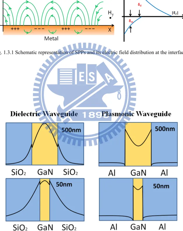
Figure 1.2 Basic structure of GaN-based LDs and LEDs...8
Figure 1.3.1 Schematic representation of SPPs and its electric field distribution at the interface...9
Figure 1.3.2 Electric Field distribution of dielectric waveguide and plasmonic waveguide...9
Figure 1.3.3 Applications of surface plasmon effect: (a) Biosensor. (b) Bioimaging. (c) Lithography (d)Nanolaser...10 Figure 2.1.1 Schematic Diagram of E-beam Lithography System...18
Figure 2.1.2 JSM-6500 E-beam Lithography System...18
Figure 2.1.3 JSM-7000F SEM System...19 Figure 2.2.1 ICP-RIE System (Oxford Plasmalab System100)...19
Figure 2.2.2 ICP-RIE System (SAMCO RIE-101PH)...20
Figure 2.2.3 E-gun Evaporation System (ULVAC EBX-8C)...20
Figure 2.3.1 Schematic Diagram of Micro-Photoluminescence System...21
Fig. 3.1.1 Process Flow Chart for Metal-coated GaN nanostripe...33
Fig. 3.1.2 SEM Image of Metal-coated GaN Nanostripe (a) Top View of the GaN Nanostripe before Deposition of Shielding Layers. (b) Angle View of One side of the GaN Nanostripe before Deposition of Shielding Layer...34
Fig. 3.1.3 Angle View of the GaN Nanostripe after the Deposition of SiO2 and Aluminum
Layers...35
Fig. 3.1.4 Schematic Diagram of Metal-coated GaN Nanostripe...35
Fig. 3.2.1 PL Spectrum of Undoped GaN Layer with and without Metal and Dielectric Shielding Layers...36
Fig. 3.2.2 PL Spectrum of Metal-coated GaN Nanostripe Above (Red) and Below (Black) Threshold...36
Fig. 3.2.3 Light-in and Light-out Curve and the Linewidth of Lasing Peak...37
Fig.3.3.1 (a) The Ez Mode Profile of the Nanostripe without Shielding Layers. (b) The Ez Mode Profile of the Nanostripe with Shielding Layers...38
Fig. 3.3.2 Schematic Diagram of the Nanostripe Model in Effective Index Method...39
Fig. 3.3.3 Effective Structure of Nanostripe under TE Mode...39
Fig. 3.3.4 TE Mode Band Diagram of Nanostripe...40
Fig. 4.1.1 Process Flow Chart for Metal-coated GaN Nanostripe...51
Fig. 4.1.2 SEM Image of different size of GaN Nanoring before shielding layer deposition (a) 7μm in diameter. (b) 5μm in diameter. (c) 3μm in diameter...52
Fig.4.1.4Schematic Diagram of Metal-coated GaN Nanostripe...53
Fig. 4.2.1 Lasing Characteristics of Metal-coated GaN Nanoring with 7μm in diameter (a)
Lasing Peak...54
Fig. 4.2.2 Lasing Characteristics of Metal-coated GaN Nanoring with 5μm in diameter (a)
Spectrum Above (Red) and Below (Black) Threshold. (b)L-L Curve and the Linewidth of the
Lasing Peak...55
Fig. 4.2.3 Lasing Characteristics of Metal-coated GaN Nanoring with 3μm in diameter (a)
Spectrum Above (Red) and Below (Black) Threshold. (b)L-L Curve and the Linewidth of the
Lasing Peak...56
Fig. A.1 The Lasing Peak Wavelength of GaN Nanoring Laser with (Red) or without (Black)
Chapter 1 Introduction
1.1 History of Semiconductor Laser
Robert N. Hall, a researcher worked for General Electric, invented first semiconductor
laser in 1962. Since then, the development of semiconductor laser had a huge progress thanks
to scientists and engineers around the globe. At 1962, Nick Holonyak Jr. demonstrated first
visible wavelength semiconductor laser at red wavelength region. Other groups in the world
also contributed to the invention of semiconductor laser in different ways.
Since invention of semiconductor laser, it promises a huge potential for its application
in the very near future. It generally becomes one of the most important types of laser in the
world. It was first used for optical communication in fiber. Then with the utilization of
different materials to fabricate the Laser Diodes (LDs), now we could see semiconductor
lasers in our daily life like optical storage, or used in a micro projector for display, even for
military purposes. Its low cost and mass-production ability make it suitable for marketing than
other types of laser.
The first laser diode was made by gallium arsenide (GaAs), which emits light from
optical communication to red wavelength region. Other types of material including gallium
nitride (GaN) also adopted to make a laser diode with a lasing wavelength from visible to
shorter wavelength region. Nowadays common lasing wavelength for laser diode is ranging
1.2 GaN-based Optoelectronic Devices
Gallium nitride (GaN) is a compound semiconductor with direct bandgap, which is a
crucial characteristic for radiative recombination. It is a wide band gap (3.4 eV) material
which makes it a suitable candidate for the application of optoelectronic devices, including
GaN-based Light Emitting Diodes (LEDs) and LDs operating in blue or ultra-violet (UV)
wavelength regions and other devices.
GaN-based LEDs fill the void on the primary color, and make white light LEDs possible
with the combination of phosphor or LED with different colors. Thanks to intensive
development in recent years [1-4], the manipulation of GaN material system has been mature
enough to create high-brightness GaN LEDs in blue wavelength. This progress makes LEDs
possible for the applications in display or solid-state lighting, and might one day replace the
light bulb which used by human beings for many years.
At the same time, GaN-based semiconductor lasers’ lasing wavelength in blue or UV
wavelength region has also developed by scientist. Since the demonstration by Nakamura et
al. [5] the first GaN-based laser lasing operated under room temperature continuous-wave
(CW) condition at 1996, many applications of GaN-based have been achieved in recent years.
Its application like blue-ray disks or as a light source in a micro-projector already exists in our
daily life.Fig. 1.2 shows typical structures of GaN-based LDs and LEDs.
developed for many years [6-9]. At 2008, T. C. Lu et al. developed GaN-based VCSELS
operated under continuous wave condition at room temperature [7]. It has some advantages
like single-longitudinal-mode operation, symmetric and low divergence angle, and two
dimensional array capabilities makes VCSELs very competitive compared with edge emitting
laser. These merits make GaN-based VCSELs have many applications in our daily life.
1.3 Surface Plasmon Effect
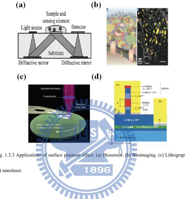
Surface plasmon polaritons (SPPS) are light waves trapped on the surface because of
electron gas couple with photons. It is a kind of electromagnetic wave propagating on the
interface between two materials which change sign on their real part of dielectric constant.
For example: a metal-dielectric interface. The SPPs existed at the interface between dielectric
materials and metal could attribute to resonant coupling of photons from the polarized light
with the oscillation of metal free electron. Fig. 1.3.1 shows the schematic representation of an
electron density wave propagating along a metal-dielectric interface and the electric field
distribution around the interface.
SPPs could concentrate and channel light under subwavelength scale, which has a huge
potential on exploring science phenomenon under such small scale, and this might one day
help scientists and engineers to make photonic integrated circuit with a smaller size than we
have now. This kind of structure also solves the problem that dielectric waveguide would
optical field for these two waveguide structures. The other advantage is surface plasmon
effect concentrates light in this way leads to an electric field enhancement that can be used to
manipulate light-matter interactions and boost non-linear phenomena. Therefore, lots of
applications have been developed for many years and exist in our daily life [10-13]. For
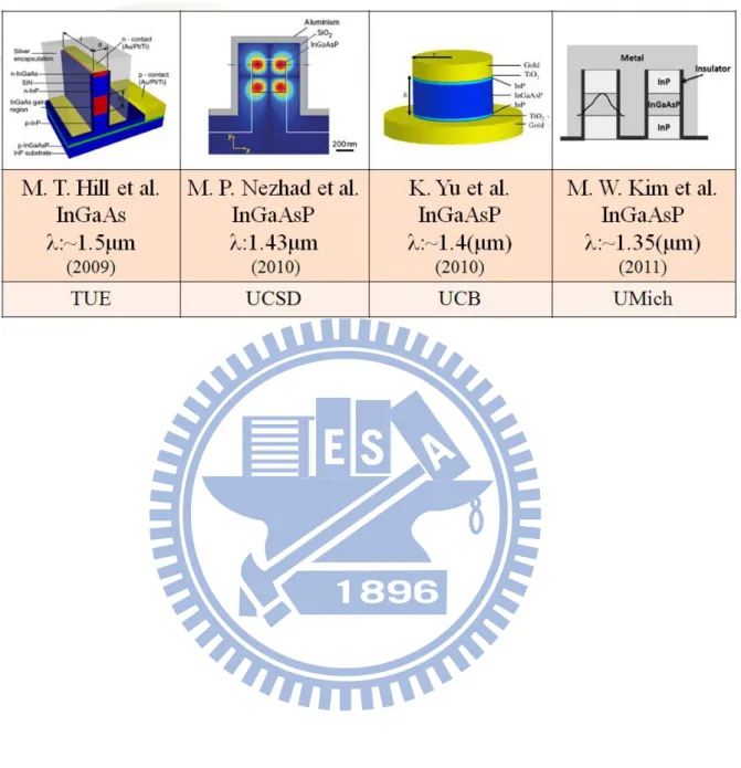
example, bioimage , biosensor , advanced lithography technique, and nanolaser.
It is the most difficult task for researchers to observe the behavior of a bio molecule.
Therefore, in order to observe this tiny molecule with the size in just a few nanometers,
researchers utilize surface plasmon effect to improve the extraction of light. With this new
technique, researchers could observe their samples and distinguish its details even in
subwavelength region. For biosensor, the utilization of surface plasmon effect makes the test
sample become label free and can be detected directly in real time. This has been applied to
drug screening, kinase analysis and research on antibody development[10]. To further lower
the cost of production for a single chip, a better lithography is needed to put more patterns on
a single wafer, the e-beam lithography and other techniques are still struggling on their
throughput, which is too low to become commercialize. A set of plasmonic mirrors takes the
advantages of surface plasmon effect and demonstrate lithography technique with a linewidth
only 80nm recently [11]. This new method has showed a promising way to the development
of nanolithography. Moreover, taking the advantages of energy confinement and field
scale even with the lossy metal coated on it [13]. Many research teams have reported their
result using different metals and cavity. This will discuss thoroughly in the following section.
Fig. 1.3.3 shows some examples of the application of surface plasmon effect.
1.4 Metal-coated Nano Devices
Metal-coated cavity has been intensely researched by scientist around the world. It could
reduce the size of a semiconductor laser to nano scale, even in subwavelength scale. This result
breaks the diffraction limit which constrains the size of a laser that cannot be smaller than its
nature wavelength. The lasing characteristics also be studied by researchers trying to explain
the physical meaning behind the experimental result.
At 2007, Martin T. Hill et al. demonstrated lasing in metal-coated nanocavity [13]. They
coated silver and dielectric layer on the nanorod and observe lasing signal at 77 K. After that,
different designs of metal-coated nanocavity have reported experimentally or theoretically.
Metal-coated waveguide structure had also been demonstrated by the same research team and
bow-tie nanostructure had been proposed by S. W. Chang et al. [14]. The combination of
surface plasmon effect and bow-tie structure shows a promising way theoretically in forming a
semiconductor laser. Moreover, different kinds of metal have been use to form metal-coated
nanocavity. From recent research results [13-17], people use silver, gold and aluminum toform
with aluminum layer and SiO2 as the dielectric layer. They also proposed a theoretical analysis
to show that optimization of the dielectric layer could have a higher chance to get a better
quality factor to achieve lasing action. K. Y. Yu et al. at 2010 demonstrated a nano-patch laser
with metal coated above and below the gain medium, and analyze the lasing characteristics of
the device [16]. In 2011, M. W. Kim et al. demonstrated lasing in a metal-clad microring [17].
In conclusion, metal-coated nanocavity has been demonstrated experimentally in different
structures includes nanorod, waveguide, and ring. In sum, recent research results mainly focus
on InGaAsP material system, which has a lasing wavelength from red to Infar-red region. Table
1.4 shows some important research results did by researchers around the world in recent years.
1.5 Motivation
Metal-coated nanocavity shows huge potential to reduce the size of semiconductor laser
into subwavelength scale. However, their research results mainly focus on InGaAsP material
system and optical communication to infra-red wavelength region. Shorter lasing wavelength
and other material systems have not yet been reported by any groups in the world.
In this thesis, we utilize GaN as the gain medium for metal-coated nanocavity, combining
with aluminum and SiO2 layer. We use E-beam lithography to define two different types of
nano structure, and then we use dry etching processes and other fabrication process to form the
devices which is optical pumped under room temperature pulsed condition, then we use finite
element method and effective index method to further simulate our structure and discuss the
physics behind the experiment result.
In chapter 2, we briefly introduce the instruments which are used to fabricate the device
and measure its characteristics. Then in chapter 3, we present experiment and simulation result
of lasing in a metal-coated GaN nanostripe at room temperature. The waveguide structure is
only 500nm in its width. In chapter 4, we use E-beam lithography to define a nanoring pattern
on the undoped GaN layer. We also perform measurement on different sizes of nanoring laser
range from 7μm to 3μm, coated with the aluminum layer. By the combination of nanoring
structure and the advantages of metal-coated nanocavity, we could shrink the size of our
nanostructure into smaller scale and better device performance. Finally in chapter 5, we will
Fig. 1.1 Dr. Robert N. Hall with Semiconductor Laser.
Fig. 1.3.1 Schematic representation of SPPs and its electric field distribution at the interface.
Fig. 1.3.3 Applications of surface plasmon effect: (a) Biosensor. (b) Bioimaging. (c) Lithography (d) nanolaser.
References
[1]S. Nakamura, M. Senoh, N. Iwasa, and S. Nagahama, “High brightness InGaN blue, green,
and yellow light-emitting diodes with quantum structures,” Jpn. J. Appl. Phys., vol. 34, pp.
L797, 1995.
[2]M. H. Kim, M. F. Schubert, Q. Dai, J. K. Kim, and E. F. Schubert, J. Piprek, and Y. Park,
“Origin of efficiency droop in GaN-based light-emitting diodes,” Appl. Phys. Lett., vol. 91,
pp. 183507, 2007.
[3]C. H. Wang, S. P. Chang, W. T. Chang, J. C. Li, Y. S. Lu, Z. Y. Li, H. C. Yang, H. C. Kuo, T.
C. Lu, and S. C. Wang, “Efficiency droop alleviation in InGaN/GaN light-emitting diodes by
graded-thickness multiple quantum wells,” Appl. Phys. Lett., vol. 97, pp. 181101, 2010.
[4]S. D. Lester, F. A. Ponce, M. G. Craford, and D. A. Steigerwald, “High dislocation
densities in high efficiency GaN-based light-emitting diodes,” Appl. Phys. Lett., vol. 66, pp.
1249, 1995.
[5]S. Nakamura, M. Senoh, S. I. Nagahama, N. Iwasa, T. Yamada, T. Matsushita, Y. Sugimoto,
and H. Kiyoku, “Room-temperature continuous-wave operation of InGaN
multi-quantum-well structure laser diodes,” Appl. Phys. Lett., vol. 69, pp. 4056, 1996.
[6]J. T. Chu, T. C. Lu, H. H. Yao, C. C. Kao, W. D. Liang, J. Y. Tsai, H. C. Kuo, and S. C.
Wang, “Room-temperature operation of optically pumped blue-violet GaN-based
pp. 2556, 2006.
[7]T. C. Lu, C. C. Kao, H. C. Kuo, G. S. Huang, and S. C. Wang, “ CW lasing of current
injection blue GaN-based vertical cavity surface emitting laser,” Appl. Phys. Lett., vol. 92,
pp. 141102, 2008.
[8]C. C. Kao, T. C. Lu, H. W. Huang, J. T. Chu, Y. C. Peng, H. H. Yao, J. Y. Tsai, T. T. Kao, H.
C. Kuo, S. C. Wang, and C. F. Lin, “The lasing characteristics of GaN-based vertical-cavity
surface-emitting laser with AlN/GaN and Ta2O5/SiO2 distributed bragg reflectors,” IEEE
Photonic Tech. Lett., vol.18, pp. 877, 2006.
[9]T. C. Lu, S. W. Chen, T. T. Wu, P. M. Tu, C. K. Chen, C. H. Chen, Z. Y. Li, H. C. Kuo, and
S. C. Wang, “Continuous wave operation of current injection GaN vertical-cavity surface
emitting laser at room temperature,” Appl. Phys. Lett., vol. 97, pp. 071114, 2010.
[10]X. D. Hoa, A. G. Kirk, M. Tabrizian, “Towards integrated and sensitive surface plasmon
resonance biosensors: A review of recent progress,” Biosensors and Bioelectronics, vol. 23,
pp. 151, 2007.
[11]W. Srituravanich, L. Pan, Y. Wang, C. Sun, D. B. Bogy, and X. Zhang, “Flying plasmonic
lens in the near field for high-speed nanolithography,” Nat. Nanotechnology vol. 3, pp. 733,
2008.
[12] M. F. Garcia-Parajo, “Optical antennas focus in on biology,” Nat. Photonics, vol. 2, pp.
[13]M. T. Hill, Y. S. Oei, B. Smallbrugge, Y. Zhu, T. de Vries, P. J. van Veldhoven, F. W. M.
van Otten, T. J. Eljkemans, J. P. Turkiewicz, H. de Waardt, E. J. Geluk, S. H. Kwon, Y. H.
Lee, R. Notzel, and M. K. Smit, “Lasing in metallic-coated nanocavities,” Nat. Photonics,
vol. 1, pp. 589, 2007.
[14]S. W. Chang, C. Y. A. Ni, S. L. Chuang, “Theory for bowtie plasmonic nanolasers,”
Opt. Express, vol. 16, pp. 10580, 2008.
[15]M. P. Nezhad, A. Simic, O. Bondarenko, B. Slutsky, A. Mizrahi, L. Feng, V. Lomakin,
and Y. Fainman, “Room-temperature subwavelength metallo-dielectric lasers,” Nat.
Photonics, vol. 4, pp. 395, 2010.
[16]K. Yu, A. Lakhani, and M.C. Wu, “Subwavelength metal-optic semiconductor nanopatch
lasers,” Opt. Express, vol. 18, pp. 8790, 2010.
[17]M. W. Kim, and P. C. Ku, “Lasing in metal-clad microring resonator,” Appl. Phys. Lett.,
vol. 98, pp. 131107, 2011.
Chapter 2 Experimental Instruments and Methods
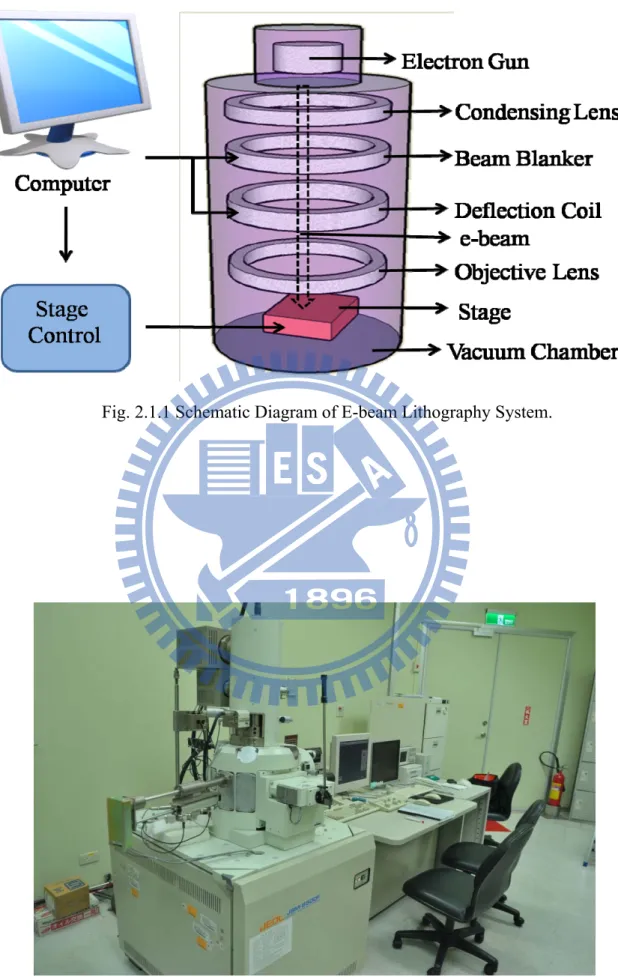
2.1 Electron Beam Lithography and Scanning Electron Microscope (SEM) Electron Beam Lithography System
Electron beam lithography, usually call as E-beam lithography, is a technique to utilize a
beam of electrons to exposing the photo resist on the surface of a material, then selectively
removing the photo resist on the film to transfer the pattern we want onto the film. This could
break the diffraction limit which constrains conventional photo lithography technique, and
shows a promising chance to fabricate device in nano-scale.
The E-beam lithography system usually consists of an electron gun as source of electron,
lenses for focusing, stage for moving the sample precisely under the electron beam, a beam
blanker to control the exposure time of electron beam and a computer to control the whole
system and the pattern. Fig. 2.1.1 shows the schematic diagram.
For most of E-beam lithography system used for commercial applications are very
expensive; therefore, for academic purpose, people usually convert an electron microscope
into an E-beam lithography system with a relatively low cost. For thesis, we use an E-beam
lithography system converted from a scanning electron microscope using JSM-6500 made by
Scanning Electron Microscope
Scanning electron microscope (SEM) is one of the most important equipment for people
to observe objects in nano-scale. The electrons interact with atoms that make up the sample
producing signals that contain information’s about itself. Moreover, preparation of the
samples for SEM is relatively easy due to the fact that SEM only require the sample to be
conductivity. The combination of higher magnification, larger depth of focus, greater
resolution, and ease of sample observation makes the SEM becomes one of the most widely
used equipment used for commercial and research purposes. Fig. 2.1.3 shows the JSM-7000F
made by JEOL.
2.2 Dry Etching Process and E-gun Evaporation Dry Etching Process
Dry etching process is critical for scientists to fabricate the device according to their
plan, and there are two types of etching processes: wet etching and dry etching. Dry etching
process uses plasma to etch the semiconductor material and it is a kind of anisotropic etching
process. The linewidth of dry etching process is smaller than wet etching, therefore, dry
etching process gradually replace wet etching process after 1980.
diffuse to chamber under ultra-low pressure. Second, when the pressure is stable, plasma is
produced by RF frequency. Third, the radicals produced by bombardment of high speed
electron would diffuse to the wafer and attach to its surface. Fourth, with the help of ion
bombardment, these radicals would react with the atoms on the surface and form by-product
as gas. At the end, these volatile by-products would then leave the surface of wafer and
discharge from chamber. Fig. 2.2.1 shows the inductively coupled plasma and reactive ion
etching (ICP-RIE) system used to etch Si3N4 layer to transfer the patter from PMMA layer,
and Fig. 2.2.2 shows the ICP-RIE equipment used to etch GaN layer.
E-gun Evaporation
E-gun evaporation, also called as E-beam evaporation, is one kind of physical vapor
deposition (PVD). The difference of E-gun evaporation is that it uses electron beam to heat
up the source material. The advantage of E-gun evaporation is that it could heat only one
small part of the surface of the source material. This will reduce the energy consumption
used by PVD. Therefore, it is a common way to use E-gun evaporation to deposit metal on to
the device.
For an E-gun evaporation system, it consists of an electron beam evaporation gun, a
system controller, power supply, evaporation material, its crucibles, and sample to be coated.
All the processes are conducted under very low pressure, in a vacuum chamber. Fig. 2.2.3
2.3 Micro-Photoluminescence (μ-PL) System
Micro-Photoluminescence is an advanced Photoluminescence system to measure
sample in micrometer even nanometer scale. The spot size of the light source for μ-PL
system has shrunk to micrometer scale to observe the optical properties of sample. In our
μ-PL system, we use Nd:YVO4 laser with lasing wavelength 355nm as a pumping source,
and the spot size is about 50 μm, frequency of the laser is 1 kHz, and the pulse width is
Fig. 2.1.1 Schematic Diagram of E-beam Lithography System.
Fig. 2.1.3 JSM-7000F SEM System.
Fig. 2.2.2 ICP-RIE System (SAMCO RIE-101PH).
Chapter 3 Lasing in Metal-coated GaN Nanostripe at Room Temperature
3.1 Epitaxial Characteristics and Fabrication Process of Metal-coated GaN Nanostripe
We use undoped GaN layer grown on C-plane (0001) sapphire substrate as gain
medium. The thickness of the undoped GaN layer is about 2μm. Metal-organic chemical
vapor deposition (MOCVD) system (EMCORE D-75) is used to grow undoped GaN layer
on the polished optical-grade C-plane (0001), 2 inches sapphire substrate. Trimethygallium
(TMGa) and Ammonia (NH3) were used as the Ga and N sources respectively.
First, a thermal cleaning process was carried out at 1080℃ for 10 minutes in a stream
of hydrogen ambient before the growth of epitaxial layers to clean the sample surface.
Second, the 30nm thick GaN nucleation layer was first grown on the sapphire substrate at
530℃, and at the end the 2μm thick undoped GaN layer was grown on it at 1040℃.
After we finish the preparation of sample, we adopt some fabrication processes to
complete our device. The complete process flow chart for our device is shown in Fig. 3.1.1.
First, we deposit 300nm thick Si3N4 layer on the undoped GaN layer as an etching mask for
the following E-beam lithography process. Second, for E-beam lithography process, we use
spin coater to put a thin polymethylmethacrylate (PMMA) on the sample, then the nanostripe
pattern was defined using E-beam lithography system. After this, we use ICP-RIE dry
etching system to transfer the pattern on the PMMA layer onto the Si3N4. And then transfer
3.1.2 shows the SEM image of nanostripe from top view and angled view after these
processes.
Third, before we start to do the next step, we use wet etching methods to clean our
sample, washing away the particles created in the previous dry etching processes to promote
the performance of our device. After this, we use plasma enhanced chemical vapor
deposition (PECVD) to deposit a thin SiO2 layer on the GaN nanostripe for just 20nm. At
the end, we use E-gun evaporation to deposit a 60nm thick aluminum layer to complete our
device. The SEM image of our device after the deposition of dielectric layer and metal is
shown in Fig. 3.1.3 in angled view. The detail recipe of each process is shown in the
following paragraphs, and the schematic diagram of metal-coated GaN nanostripe is shown
in Fig. 3.1.4. PECVD (SAMCO PD220) z Si3N4 film deposition: SiH4/Ar: 20sccm NH3:10sccm N2:490sccm Temperature: 300℃ RF Power: 35W Pressure: 100Pa
Time: 31min. for 300nm thick Si3N4
z SiO2 film deposition:
SiH4/Ar: 25sccm N2O:500sccm N2:250sccm Temperature: 250℃ RF Power: 35W Pressure: 120Pa
Time: 1min. for 20nm thick SiO2
ICP-RIE (Oxford Plasmalab System 100)
z Si3N4 film etching: Ar/O2: 5sccm CHF3: 50sccm RF Power: 150W Pressure: 7.5x10⁻⁹Torr Temperature: 20℃
Time: 3min. 40sec. to etch 300nm thick Si3N4 film
ICP-RIE (SAMCO RIE-101PH)
Cl2: 25sccm
Ar: 10sccm
ICP Power: 200W
Bias Power: 200W
Pressure: 0.33Pa
Time: 55sec. to etch 500nm thick GaN film
E-beam Lithography System (JEOL JSM-6500)
z Spin coating use PMMA (A5)
First step: 1000 rpm for 10sec.
Second step: 3500 rpm for 25sec.
z Hard bake: hot plate 180℃, 90sec.
z Exposure:
Beam voltage: 25KeV
Dosage: 1.4~1.7 (point does)
z Development: MIBK: IPA (1:3) 70sec.
z Fixing: IPA 40sec.
z Source: Aluminum
z Pressure: 3x10⁻⁶Torr
z Current: 170mA for first 5nm
200mA for the rest 55nm
z Pressure: 3x10⁻⁶Torr
3.2 Lasing Characteristics of Metal-coated GaN Nanostripe at Room Temperature
To explore experimentally about our device, we use the micro-Photoluminescence
system mentioned in the previous chapter to measure its characteristics. We pump our device
directly from the metal side to avoid the absorption of undoped GaN layer beneath our
device, if we choose to pump the device from the back of the wafer.
First, to ensure that the lasing action is truly originated from our nano structure, we use
a He-Cd 325nm continuous-wave laser to pump the flat region of undoped GaN layer, before
and after the deposition of dielectric layer and metal to see the Photoluminescence (PL)
spectrum of them. As shown in Fig. 3.2.1, the peak wavelength of undoped GaN layer is
about 362nm. However, the spectrum after the deposition of SiO2 and aluminum layer is
totally different, the peak around 362nm no longer exists because the energy from 350nm to
380nm had been totally absorbed by shielding layer. Therefore, we could use Fig. 3.2.1 to
PL spectrum of the metal-coated nanostripe below (black) and above (red) the threshold
power density has been presented. This device has a single lasing mode at 370nm and the
difference between two spectrums further ensure that we observe a lasing action in our
structure. From the light-in light-out curves of this mode shows in Fig. 3.2.3 and the
linewidth of the lasing mode, we could observe linear behavior after soft turn-on which
indicates the lasing action, and also the narrowing linewidth shows that the transition from
spontaneous emission to stimulated emission of the optical mode. These evidences prove the
lasing action in our metal-coated GaN nanostripe. The threshold pump power density is
about 0.055kW/cm2 (55mJ/cm2) and the quality factor estimated by the wavelength to
linewidth around the transparency is 150. Compared to the sample without metal or SiO2
shielding layer, the high thermal conductivity and high reflectivity of aluminum make
measurement easier and increase the possibility of lasing at room temperature. Moreover, the
SiO2 layer would passive the surface roughness created by the dry etching processes and
therefore reduce the nonradiative center on the surface of the nanostripe, and it reduce
energy loss if the metal layer is directly coated on to the gain medium, this would reduce the
absorption and lower the threshold gain of this device, making lasing action possible [1].
The nanostripe without shielding layer exhibits high optical loss and lower Q value. It was
for these reasons that we can’t observe lasing action in uncoated GaN nanostripe. The
metal-coated device is that aluminum has a higher reflectivity which could show a better
optical confinement at UV wavelength region compared with silver [2], even aluminum is
also quite lossy at this wavelength region. Also, the adhesive ability to SiO2 is better for
aluminum than gold.
3.3 Simulation Results and Discussion
To get a better understanding of our experiment results, we use finite-element-method
(FEM) to simulate the optical mode in our metal-coated nanocavity. The simulation model
consists of a sapphire layer, an undoped GaN layer, a thin SiO2 layer, and an aluminum
shielding layer. The refractive indexes of aluminum and undoped GaN layers established by
Peng and Piprek[3], and Rakic et al. [4], with the refractive index of the SiO2 are 1.46. This
model also includes a perfectly matched layer surrounds the nanocavity to absorb redundant
signal which might reflect back to the metal-coated nanocavity, thereby influencing the
simulation result. Fig.3.3.1 shows the simulated optical mode profiles for a GaN nanostripe
cavity with or without the shielding layers. In Fig.3.3.1 (a), the model incorporating metal
and SiO2 layers had an optical mode well confined within the nanostripe, demonstrating a
clear standing wave pattern with 3.5 nodes. However, for the nanostripe without shielding
layers in Fig. 3.3.1 (b), the optical mode leaks into the region of air with a standing wave
pattern lacked uniformity, compares with the metal-coated nanostripe. The wavelength of the
ten times larger than the case in Fig. 3.3.1 (b). This illustrates the difficulty of achieving
GaN nanostripe lasing without dielectric and metal layer coated on it. The small differences
between the experimental and simulation results might comes from the imprecise fabrication
processes and the imprecision of material indices used in the simulation model. From the
discussion above, we confirmed that the metal shielding layer in this structure plays an
important role in lasing at room temperature. And also, from the thermal conductivity of
aluminum (237W/m-k) and air (0.025W/m-k), it indicates that under room temperature
pulsed condition, metal-coated nanostripe has a better opportunity to observe lasing action
before it breaks down than the nanostripe without shielding layers.
To further improve the performance of this device, vertical confinement would be the
key issue. Distributed Bragg Reflector (DBR) would significantly reduce the energy loss
from the bottom of the nanostripe as shown in Fig. 3.3.1 (a). For example, C. Y. Lu et al.
demonstrated this idea by an n-type DBR with metal coated on the microrod [5]. The device
operated under room temperature continuous-wave condition, and showed a high thermal
resistance. This would form a three dimensional cavity which would definitely improve the
performance of the device and even operate under electrically pumped condition. Also,
heterostructure with precise calculation to confine the optical field in the active region would
Moreover, we adopt effective index method to calculate the band diagram of this
structure. The effective index method is an efficient method to analysis rectangular
waveguide structure, which is really common structure for semiconductor laser. The ridge
waveguide structure has been split into different part first, and calculates the effective
indexes of each part, then combined these parts together again and calculate the true
effective index of this structure. A representation schematic diagram is shown in Fig. 3.3.2.
This way put the complex two dimensional calculations into one dimensional, and still keeps
a high accuracy with the experimental result. In our case, we split our nanostripe structure
into three parts as shown in Fig. 3.3.3 and then calculate the band diagram. The TE mode
band diagram is shown in Fig. 3.3.4, as you could see, there is only one waveguide band in
this structure. Moreover, around 370nm there is waveguide mode quite fit to our
experimental result. We believe that the single mode lasing we observe in the experiment is
a combination of TE waveguide mode with surface plasmon mode from the Al/SiO2/GaN
interfaces. The calculation helps us to clarify the observation result and further prove that
there would be only one optical mode with a clear standing wave pattern confine in the
nanostripe, which makes lasing action possible.
3.4 Summary
In sum, we demonstrated lasing in metal-coated GaN nanostripe at room temperature
was about 370nm and the threshold power density is about 0.055kW/cm2. The quality factor
was about 150 estimated from the experimental result. FEM simulation result showed the
importance of aluminum layer coated on the nanostripe in the lasing action, and from
effective index method, the single mode lasing was confirmed by the band diagram of the
nanostripe structure, which had only one waveguide band around 300nm to 400nm
wavelength region. From experimental and simulation results, the GaN nanostripe without
metal and SiO2 shielding layers was really hard to achieve lasing at room temperature with
the width of the nanostripe only 500nm due to its poor optical confinement and worse
Fig. 3.1.2 SEM Image of Metal-coated GaN Nanostripe (a) Top View of the GaN
Nanostripe before Deposition of Shielding Layers. (b) Angle View of One side of the GaN
Fig. 3.1.3 Angle View of the GaN Nanostripe after the Deposition of SiO2 and
Aluminum Layers.
Fig. 3.2.1 PL Spectrum of Undoped GaN Layer with and without Metal and Dielectric Shielding Layers.
360
370
380
390
400
410
420
0.0
0.2
0.4
0.6
0.8
1.0
Intensity (a.u.)
Wavelength (nm)
0.015kW/cm
2
0.065kW/cm
2
Fig. 3.2.2 PL Spectrum of Metal-coated GaN Nanostripe Above (Red) and Below (Black)
0.00
0.02
0.04
0.06
0.08
0.0
0.2
0.4
0.6
0.8
1.0
Pump Power Density (kW/cm
2)
Intensity (a.u.)
0
2
4
6
8
10
Linewidth (nm)
(a)
(b)
Fig.3.3.1 (a) The Ez Mode Profile of the Nanostripe without Shielding Layers. (b) The
y
z
Fig. 3.3.2 Schematic Diagram of the Nanostripe Model in Effective Index Method.
References:
[1] A. Mizrahi, V. Lomakin, B. A. Slutsky, M. P. Nezhad, L. Feng, and Y. Fainman, “Low
threshold gain metal coated laser nanoresonators,” Opt. Lett., vol. 33, pp. 1261, 2008.
[2] W. M. Rohsenow and H. Choi, “Heat Mass and Momentum Transfer,” Prentice Hall,
New York, (1961).
[3]T. Peng, and J. Piprek, “Refractive index of AlGaInN alloys,” Electron. Lett., vol. 32, pp.
2285, 1996.
[4]A. D. Rakic, A. B. Djurisic, J. M. Elazer, and M. L. Majewski, “Optical properties of
metallic films for vertical-cavity optoelectronic devices,” Appl. Opt., vol. 37, pp. 5271,
1998.
[5]C. Y. Lu, S. W. Chang, S. L. Chuang, T. D. Germann, and D. Bimberg, “Metal-cavity
surface-emitting microlaser at room temperature,” Appl. Phys. Lett., vol. 96, pp. 251101,
2010.
[6]M. T. Hill, “Status and prospects for metallic and plasmonic nanolasers,” J. Opt. Soc. Am.
Chapter 4 Lasing in Metal-coated GaN Nanoring at Room Temperature
4.1 Epitaxial Characteristics and Fabrication Process of Metal-coated GaN Nanoring
We use undoped GaN layer grown on C-plane (0001) sapphire substrate as gain
medium. The thickness of the undoped GaN layer is about 2μm. Metal-organic chemical
vapor deposition (MOCVD) system (EMCORE D-75) is used to grow undoped GaN layer
on the polished optical-grade C-plane (0001), 2 inches sapphire substrate. Trimethygallium
(TMGa) and Ammonia (NH3) were used as the Ga and N sources respectively.
First, a thermal cleaning process was carried out at 1080℃ for 10 minutes in a stream
of hydrogen ambient before the growth of epitaxial layers to clean the sample surface.
Second, the 30nm thick GaN nucleation layer was first grown on the sapphire substrate at
530℃, and at the end the 2μm thick undoped GaN layer was grown on it at 1040℃.
After we finish the preparation of sample, we adopt some fabrication processes to
complete our device. The complete process flow chart for our device is shown in Fig. 4.1.1.
First, we deposit 300nm thick Si3N4 layer on the undoped GaN layer as an etching mask for
the following E-beam lithography process. Second, for E-beam lithography process, we use
spin coater to put a thin polymethylmethacrylate (PMMA) on the sample, then the nanostripe
pattern was defined using E-beam lithography system. After this, we use ICP-RIE dry
etching system to transfer the pattern on the PMMA layer onto the Si3N4. And the transfer
4.1.2 shows the SEM images of different size of nanorings from angled view after these
processes.
Third, before we start to do the next step, we use wet etching method to clean our
sample, washing away the particles created in the previous dry etching processes to promote
the performance of our device. After this, we use E-gun evaporation to deposit a 50nm thick
aluminum layer to complete our device. Fig. 4.1.3 shows one of the nanorings after metal
deposition. The detail recipe of each process is shown in the following paragraphs, and the
schematic diagram of metal-coated GaN nanoring is shown in Fig. 4.1.4.
PECVD (SAMCO PD220) z Si3N4 film deposition: SiH4/Ar: 20sccm NH3:10sccm N2:490sccm Temperature: 300℃ RF Power: 35W Pressure: 100Pa
Time: 31 min for 300nm thick Si3N4
ICP-RIE (Oxford Plasmalab System 100)
Ar/O2: 5sccm
CHF3: 50sccm
RF Power: 150W
Pressure: 7.5x10⁻⁹Torr
Temperature: 20℃
Time: 3min. 35sec. to etch 300nm thick Si3N4 film
ICP-RIE (SAMCO RIE-101PH)
z GaN film etching:
Cl2: 25sccm
Ar: 10sccm
ICP Power: 200W
Bias Power: 200W
Pressure: 0.33Pa
Time: 65sec. to etch 600nm thick GaN film
E-beam Lithography System (JEOL JSM-6500)
z Spin coating use PMMA (A5)
First step: 1000 rpm for 10sec.
Second step: 3500 rpm for 25sec.
z Exposure:
Beam voltage: 25KeV
Dosage: 1.4~1.7 (point does)
z Development: MIBK: IPA (1:3) 70sec.
z Fixing: IPA 40sec.
E-gun Evaporation System (ULVAC EBX-8C)
z Source: Aluminum
z Pressure: 3x10⁻⁶Torr
z Current: 170mA for first 5nm
200mA for the rest 55nm
z Pressure: 3x10⁻⁶Torr
4.2 Lasing Characteristics of Metal-coated GaN Nanoring at Room Temperature
To investigate the performance of our metal-coated GaN nanoring device, we use the
micro-Photoluminescence system mentioned in chapter 2 to measure the lasing characteristics
of our devices. We directly pump our device at room temperature, trying to avoid absorption
In our experiment, there are three different sizes of nanoring structure: 7μm, 5μm, and
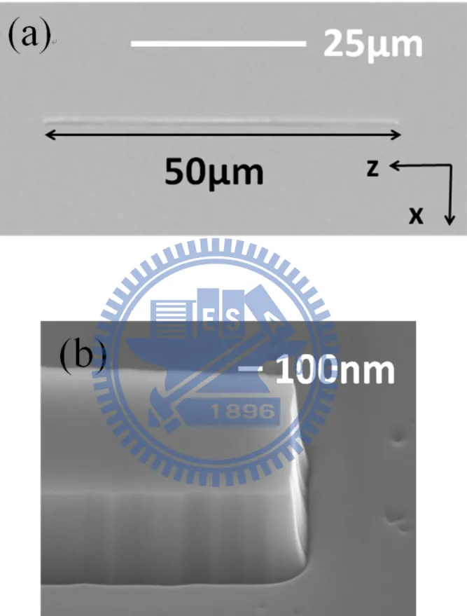
3μm in diameter. Fig. 4.2.1 to Fig. 4.2.3 shows the lasing characteristics of metal-coated
nanorings with different diameter. The smallest nano structure we observe lasing action is the
nanoring structure with 3μm in diameter, 600nm in height, and 310nm in width. The width of
this structure is below the nature wavelength of the lasing mode. Due to better control of dry
etching processes, there is no SiO2 layer between metal and gain medium for nanoring
structure, trying to utilize the advantages of surface plasmon effect as much as possible.
Following paragraphs are the lasing characteristics of our nanoring devices.
For metal-coated GaN nanoring with 7μm in diameter, we observe a lasing action with
lasing wavelength around 365nm, which is shown in Fig. 4.2.1 (a). The spectrum above (red)
and below (black) the threshold for our nano structure clearly indicate that we observe a
lasing action. From Fig, 4.2.1 (b), the threshold pump power density is 0.019 kW/cm2
(19mJ/cm2) obtained from the experimental result. Moreover, the quality factor estimated by
the ratio of wavelength to linewidth around the transparency is about 910. We believe this
high quality factor could attribute to the combination of whispering-gallery mode and surface
plasmon mode. This is the reason why we could still observe lasing action even though we
shrink the size of our device to a smaller scale.
We further shrink the diameter of the nanoring to 5μm, and the width of the nanoring to
characteristics are shown in Fig. 4.2.2. The lasing peak is around 363nm, as we could see that
the spectrum above and below the threshold for this structure is quite different. For this case,
the threshold pump power density is about 0.042kW/cm2 (42mJ/cm2), and the quality factor is
about 910, which is quite the same as the result of metal-coated GaN nanoring in the previous
paragraph. Clear turn-on behavior of L-L curve and the narrowing linewidth of the lasing
peak after turn-on both indicate the lasing action at room temperature.
At last, the smallest nanoring structure which we could observe lasing action at room
temperature is 3μm in diameter, 600nm in height, and 310nm in width. It is the best result we
could obtain under room temperature, pulsed condition. For this case, the lasing wavelength is
364nm and the quality factor is about 800. The difference in quality factor of our device might
be due to the smaller device, the stronger interaction between metal and gain medium is under
such a small scale. The threshold pump power density is around 0.045kW/cm2 (45mJ/cm2)
estimated from the L-L curve shown in Fig. 4.2.3 (b). The increase in threshold power density
might be due to the beam spot size of our micro-PL system is about 50μm, which is much
larger than the nanoring device. Poor injection efficiency might be the reason for increasing
threshold power when we have smaller device. Table 4.2 shows the lasing characteristics and
the geometric parameter of our device.
4.3 Result and Discussion
utilize whispering-gallery mode which do not require other feedback structure to form the
cavity [1]. Therefore, metal layer coated on the nanoring structure could be specifically used
to reduce optical loss from the side of the nanoring structure and makes lasing action possible
at room temperature. Higher quality factor is expected for nanoring structure compare to
waveguide structure. Higher quality factor indicates that photon in this structure would stay
longer and have higher chance to get enough gain from the gain medium to overcome the loss.
The experiment result of metal-coated GaN nanoring laser confirms our hypothesis. Even
though both nano structures are benefit from better optical confinement and better thermal
conductivity which make lasing action possible at room temperature, the advantages of
whispering-gallery-mode make the device performance of nanoring better than nanostripe
structure. Moreover, these advantages let us could shrink our device to smaller scale compare
to the nanostripe structure. We could still observe lasing action at room temperature with the
width of the nanoring down to subwavelength scale, which is not possible for nanostripe case.
Table 4.3 lists a comparison between nanostripe and nanoring structure.
As shown in the Table 4.3, the size of the nano structure has reduced significantly.
Compare to nanostripe structure, which has a size about 12.5μm3, the size of the smallest
nanoring structure we could observe lasing action at room temperature is 1.7μm3, seven times
smaller than the nanostripe structure. Moreover, the width of the nanoring has been shrunk
achieve lasing in such a thin structure in nanostripe case. We believe that the utilization of
whispering-gallery mode would be the key reason for this result.
Moreover, compare to the lasing characteristics of these two devices, the nanoring
structure has a lower threshold power density and higher quality factor. The quality factor is
about 6 times larger for nanoring structures which are 5 or 7μm in diameter, and about 5.5
times for nanoring structure which is 3μm in diameter. The threshold power density is at least
20% lower for the nanoring structure compare to the nanostripe structure.
In conclusion, whispering gallery mode would be a better choice to further improve the
performance of metal-coated nanocavity than fabry-perot oscillation from the waveguide
structure.
4.3 Summary
Even though some research results about metal-clad microring laser already reported
experimentally and theoretically [1,4], they only observed lasing action at 77K and the quality
factor was about 160, which was quite similar to other structure reported previously [5-7].
The advantages of whispering-gallery mode weren’t fully utilized by them. Therefore, in our
experiment, we demonstrate lasing in metal-coated GaN nanoring at room temperature. It is
the first time in the world that demonstrates lasing in metal-coated nanoring cavity at room
temperature with GaN-based material system with such a high quality factor.
diameter. They all could observe lasing action at room temperature by optical pumping.
Besides, their quality factors are about 800 to 900, much higher than previous reported data.
The lasing wavelength of each device is 365nm, 363nm, and 364nm, and the threshold power
density for each one is 0.019kW/cm2 (19mJ/cm2), 0.042kW/cm2 (42mJ/cm2), and
0.045kW/cm2 (45mJ/cm2) respectively.
Compare to the nanostripe structure mentioned in the previous chapter, nanoring
structure has higher quality factor and lower threshold power density than it. We could further
shrink the volume of the device to one tenth the nanostripe structure, and the width of the
nanoring is smaller than the lasing wavelength. We attribute this result to better feedback
mechanism brought by nanoring structure. Moreover, from the experimental result, the
red-shift of lasing peak wavelength of the reference sample compares to the metal-coated one
which shows a steady blue-shift as pumping power increase indicates that metal could provide
better thermal dissipation than the air, so the device’s performance won’t be influenced by
Fig. 4.1.2 SEM Image of Different Size of GaN Nanoring before Shielding Layer
Deposition (a) 7μm in diameter. (b) 5μm in diameter. (c) 3μm in diameter.
Fig. 4.2.1 Lasing Characteristics of Metal-coated GaN Nanoring with 7μm in diameter (a) PL
Spectrum Above (Red) and Below (black) Threshold. (b) L-L Curve and the Linewidth of the
Fig. 4.2.2 Lasing Characteristics of Metal-coated GaN Nanoring with 5μm in diameter (a) PL
Spectrum Above (Red) and Below (black) Threshold. (b) L-L Curve and the Linewidth of the
Fig. 4.2.3 Lasing Characteristics of Metal-coated GaN Nanoring with 3μm in diameter (a) PL
Spectrum Above (Red) and Below (black) Threshold. (b) L-L Curve and the Linewidth of the
Table 4.2 Lasing Characteristics of Different Metal-coated GaN Nanorings.
References:
[1] M. W. Kim, and P. C. Ku, “Lasing in metal-clad microring resonator,” Appl. Phys. Lett.,
vol. 98, pp. 131107, 2011.
[2] C. Y. Lu, S. W. Chang, S. H. Yang, and S. L. Chuang, “Quantum-dot laser with a
metal-coated waveguide under continuous-wave operation at room temperature,” Appl.
Phys. Lett., vol. 95, pp. 233507, 2009.
[3] C. Y. Lu, S. W. Chang, S. L. Chuang, T. D. Germann, and D. Bimberg, “Metal-cavity
surface-emitting microlaser at room temperature,” Appl. Phys. Lett., vol. 96, pp. 251101,
2010.
[4] M. W. Kim, and P. C. Ku, “The metal-clad semiconductor nanoring laser and its scaling
Chapter 5 Conclusion 5.1 Conclusion
Lasing in metal-coated GaN nanocavity at room temperature is demonstrated. With the
combination of GaN as gain medium and metal-coated nanocavity, lasing signal has been
observed at room temperature in nanostripe and nanoring structure.
First, we observe a lasing peak with its wavelength is about 370nm and the quality factor
is 150 for our metal-coated GaN nanostripe. It has a low threshold pump power density which
is only 0.055kW/cm2 (55mJ/cm2). Moreover, by finite element method and effective index
method, we prove that the aluminum layer coated on the nanostripe provides a better optical
confinement and better thermal conductivity makes lasing action possible at room temperature
and single mode lasing has been confirmed by the band diagram of the nanostripe structure
and all these simulation results fit to experimental result pretty with only a small difference
between them.
Second, we conduct fabrication process to make metal-coated GaN nanoring laser. The
smallest ring we could observe lasing action at room temperature is 3μm in diameter, and the
widths of the nanorings is about 310nm, smaller than the lasing wavelength. The quality
factor of this device is about 800 and the threshold power density is only 0.045kW/cm2
(45mJ/cm2). Better performance and smaller device are obtained by the combination of
power density is smaller compare to metal-coated nanostripe. Also, better thermal stability of
metal-coated device is confirmed by analyzing the PL spectrum of the devices. All these
results shows promising way to further improve the device performance and shrink the size of
device into subwavelength-scale.
5.2 Future Work
In order to achieve lasing in three-dimensional nanocavity or operate under
electrically-pump condition, we have to reduce the optical loss in vertical direction. As shown
in chapter 3, even though we could see clear standing wave pattern in the nanostripe structure,
there is still some energy dissipate into the undoped GaN region beneath the structure. If we
wanted to further improve device performance, we have to improve optical confinement
vertically by heterostructure or Distributed Bragg reflector (DBR).
Moreover, poor injection efficiency of the measurement system might reduce the device
performance. First, the beam spot size of Nd:YVO4 laser is about 50μm, which is much larger
than our device, lots of energy is wasted and might be the reason why there is always a signal
around 370nm to 380nm in our spectrum. Smaller beam spot size comparable to the size of
our device would significantly increase injection efficiency and the threshold power density
might be smaller than what we get right now. Second, if we could use bonding technique to
remove the sapphire substrate and undoped GaN layer beneath the device, we could collect
signal from top of the wafer, where is coated a high-reflectivity metal layer.
All the issues mentioned in the previous paragraphs are the key points for further
development of metal-coated nanocavity. If we could solve these problems, we could achieve
lasing in three dimensional or subwavelength nanocavity and photonic integrated circuit in
Appendix
1. Thermal Issue
The thermal conductivity of metal is better than the air, therefore, it is believed that the
device with metal layer coated on it would show a better performance after reduce the thermal
effect. In our cases, the aluminum layer’s thermal conductivity (237W/m-K) coated on the
GaN nanocavities is far better than air (0.025W/m-K). We believe that this is also an
important feature provided by metal so that we could observe lasing action at room
temperature. From the lasing characteristics of GaN nanoring with and without metal, 5μm in
diameter, we could observe the differences brought by metal layer.
From the PL spectrum, the lasing peak of the metal-coated nanolaser has a blue shift as
the pumping power increase. However, for the GaN nanoring, 5μm in diameter, it has a red
shift after a small blue shift as the pumping power increase, this indicates that the heat
provided by pumping source influence the device performance. We believe that it is the metal
layer coated on the nanoring structure passivates the heat provided by the pumping source, so
that the device performance won’t be affected by it. Fig. A. 1 shows the lasing peak
wavelength of these two devices after turn on. This evidence shows that the metal layer
coated on the nanocavity not only provide better optical confinement, but also better thermal
dissipation that the device performance won’t be influenced by heat even operate at high
Fig. A.1 The Lasing Peak Wavelength of GaN Nanoring Laser with (Red) or without (Black) Metal.