行政院國家科學委員會專題研究計畫 期中進度報告
利用奈米碳管製造低電壓操作之場發射顯示器之製程研究
(2/3)
計畫類別: 個別型計畫 計畫編號: NSC91-2215-E-009-057- 執行期間: 91 年 08 月 01 日至 92 年 07 月 31 日 執行單位: 國立交通大學電子工程學系 計畫主持人: 鄭晃忠 計畫參與人員: 阮全平,林高照,蔡春乾 報告類型: 精簡報告 處理方式: 本計畫可公開查詢中 華 民 國 92 年 5 月 30 日
行政院國家科學委員會補助專題研究計畫
□ 成 果 報
告 ▓期
中進度
報
告
利用奈米碳管製造低電壓操作之場發射顯示器之製程
研究
計畫類別:▓ 個別型計畫 □ 整合型計畫
計畫編號:NSC 91-2215-E-009-057-
執行期間: 91 年 08 月 01 日至 92 年 07 月 31 日
計畫主持人: 鄭晃忠
共同主持人:
計畫參與人員: 阮全平、林高照、蔡春乾
成果報告類型(依經費核定清單規定繳交):▓精簡報告 □完整
報告
本成果報告包括以下應繳交之附件:
□赴國外出差或研習心得報告一份
□赴大陸地區出差或研習心得報告一份
□出席國際學術會議心得報告及發表之論文各一份
□國際合作研究計畫國外研究報告書一份
處理方式:除產學合作研究計畫、提升產業技術及人才培育研究
計畫、列管計畫及下列情形者外,得立即公開查詢
□涉及專利或其他智慧財產權,□一年□二年後可公
開查詢
執行單位:
中 華 民 國 92 年 5 月 30 日
Ⅰ 中文摘要 場發射電流值的變動已成為場發射顯示器應用的重要議題。整合薄膜電晶體與碳管 發射源為一有效改善電流穩定性之法。伴隨主動控制的薄膜電晶體,其電流穩定性有著 顯著而立即的改善。其擾動值減少至兩個百分點以下,遠低於傳統結構約百分之五十的 震盪。同時,薄膜電晶體也提供了可控制及穩定的電流。 關鍵字 奈米碳管、薄膜電晶體、穩定度 AbstractEmission current fluctuation from CNTs is always observed and it becomes an important issue for applications in FED. Integration of thin-film-transistor-controlled carbon nanotube for field emission display is an effective way to improve current stability .
With an active-controlled thin-film-transistor, the results of electrical characteristics measurements revealed the improved field emission stability . The emission current fluctuation of the LC-TFT-controlled CNTs can be reduced to within 2%, below the fluctuation of uncontrolled CNTs. This TFT-controlled scheme of CNTs provides a controllable and stable emission current
Keyword
Ⅱ Report
Introduction
Field emission display (FED) has emerged as a leading contender in display technologies because it combines the best features of cathode ray tube (CRT) and flat panels. The field emitters provide cold electrons to bombard phosphors in anode plate to generate high luminance. While a significant amount of research has focused on triode-type field emitters, emission current stability remains a central problem in commercializing field emission devices. An effective way to improve current stability is to connect a constant electron source, such as a field-effect transistor (FET) or thin-film transistor (TFT), to the emitters in series [1-3]. However, the process of conventional triodes combined with the FET is more complicated and the driving/addressing voltage is still high. Recently, carbon nanotubes (CNTs) have demonstrated excellent field emission properties for future FED, due to their low electric field emission, high chemical stability, and high mechanical strength [4-6]. However, most of the CNT emitters are fabricated with a diode-type structure and the driving voltage for the diode-type CNTs is very high. Moreover, emission current fluctuation from CNTs is always observed and it becomes an important issue for applications in FED. Song has developed an active-controlled diode emitters (ACDE) structure which significantly improves the current stability of CNTs [7]. Nevertheless, the operation of Song’s design is complicated. For example, the TFT devices and CNTs were fabricated on different substrates and the drain of the TFT was connected to the cathode.
In this study, we propose and fabricate a new field emission device based on monolithic TFT-controlled CNTs. The structure is simple with the CNTs being directly synthesized on the drain region of a TFT. Meanwhile, electrons emitted from the CNTs are supplied through the inversion layer, which is produced by the field effect of a gate voltage. The long channel TFT was designed to exhibit a high-breakdown voltage and low leakage current in the OFF-state. The actively TFT-controlled CNTs can achieve excellent emission stability and low-voltage modulation of the emission current.
Results and Discussion
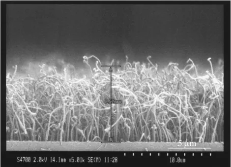
Figure 1 shows a micrograph of CNTs synthesized on the drain region of the LC-TFT via scanning electron microscopy (SEM). CNTs are uniformly distributed over the entire region and no carbonaceous particles are observed. The average height of the CNTs is about 8.5 m and their average diameter is around 100 nm to 200 nm. These nanotubes are disordered and most of them become curved at the top.
Figure 2 demonstrates the field emission properties of CNTs with and without TFT-control. The anode currents (Ia) were measured as a function of the anode voltage (Va) with various
LC-TFT gate voltages. The saturated anode currents of 2.8 A5.8 A, and 11 A were obtained at the LC-TFT gate voltages of 35 V, 40 V, and 45 V, respectively. As can be seen, the saturated anode current can be modulated by the TFT gate voltage. However, the anode current of LC-TFT-CNTs increased rapidly when the anode voltage was higher than 480 V (for Vg = 40 V). It is attributed to that the junction breakdown occurred between the drain and
gate, which was induced by a high electric field at the drain. In addition, the turn-on electric fields of the LC-TFT-controlled CNTs were raised to 2.5 V/µm owing to the high resistance of the relatively long channel and conductive path between the source and the drain. Figure 3 presents the anode current and gate voltage characteristics of the LC-TFT-controlled CNTs. The anode voltage was kept at 450 V. An ON/OFF current ratio of 103 was achieved for the gate voltage switching from 26 V to 45 V, indicating that the driving voltage of diode-type CNTs can be significantly reduced.
The emission current stability of the uncontrolled CNTs and LC-TFT-controlled CNTs are compared in Fig. 4. Different current levels of the LC-TFT-controlled CNTs at different gate voltages were tested over a period of 1 h. All of the stress conditions exhibit stable emission characteristics with a fluctuation of less than 2% for the LC-TFT-controlled CNTs. In contrast, the uncontrolled CNTs show a larger current fluctuation of about 50%. This result demonstrates that the TFT-control significantly improves the field emission stability of CNTs
Conclusions
We have developed a new device scheme of CNTs incorporating a LC-TFT. CNTs are directly integrated in the drain region of the LC-TFT, and the TFT can modulate the emission current from CNTs. The well saturated anode currents of 2.8 A5.8 A, and 11 A were obtained at the TFT gate voltages of 35 V, 40 V, and 45 V, respectively. An ON/OFF current ratio of 103 can be achieved with the gate voltage switching from 26 V to 45 V. The emission current fluctuation of the LC-TFT-controlled CNTs can be reduced to within 2%, below the fluctuation of uncontrolled CNTs. This TFT-controlled scheme of CNTs provides a controllable and stable emission current, and has great potential for future applications in field emission display and vacuum microelectronics.
Reference
[1] K. Yokoo, M. Arai, M. Mori, J. Bae, and S. Ono, “Active control of the emission current of field emitter arrays,” J. Vac. Sci. & Technol. B, Vol. 13, p. 491, 1995.
[2] T. Hirano, S. Kanemaru, H. Tanoue and J. Itoh, “Fabrication of a new Si field emitter tip with metal-oxide-semiconductor field-effect transistor (MOSFET) structure,” Jpn. J.
Appl Phys., Vol. 35, p. 6637, 1996.
[3] G. Hashiguchi, H. Mimura, and H. Fujita, “Monolithic fabrication and electrical
characteristics of polycrystalline silicon field emitters and thin film transistor,” Jpn. J. Appl Phys., Vol. 35, p. L84, 1996.
[4] T. W. Ebbesen, “CARBON NANOTUBES” (CRC Press, Boca Raton, 1997).
[5] J. H. Han, W. S. Yang, J. B. Yoo, and C. Y. Park, “Growth and emission characteristics of vertically well-aligned carbon nanotubes grown on glass substrate by hot filament plasma-enhanced chemical vapor deposition,” J. Appl Phys., Vol. 88, p. 7363, 2000. [6] V. I. Merkulov, D. H. Lowndes, and L. R. Baylor, “Scanned-probe field-emission studied
of vertically aligned carbon nanofibers,” J. Appl Phys., Vol. 89, p. 1933, 2001. [7] Y. H. Song, D. H. Kim, S. W. Lee, S. K. Lee, M.Y. Jung, S. Y. Kang, Y. R. Cho, J. H.
Lee, and K. I. Cho, Tech. Digest of Society for Information Display, L-3, p. 1252, 2000.
[8] T. Unagami and O. Kogure, “High voltage TFT fabricated in recrystallized polycrystalline silicon,” IEEE Trans. Electron Devices, Vol. 35, p. 314, 1988.
[9] T. Serikawa, S. Shirai, A. Okamoto, and S. Suyama, “Low temperature fabrication of high-mobility poly-Si TFT’s for large-area LCD’s”, IEEE Trans. Electron Devices, Vol. 36, p. 929, 1989. 0 100 200 300 400 500 0 2 4 6 8 10 12 Uncontrolled carbon nanotubes Vg = 35 V Vg = 40 V Vg = 45 V TFT-controlled A no d e c ur re nt ( A ) Anode voltage, Va (V)
Fig. 1 SEM image of CNTs synthesized on the drain region of the LC-TFT.
5 m
Fig. 2 Anode current versus anode voltage for uncontrolled and LC-TFT-controlled CNTs.
25 30 35 40 45 10-9 10-8 10-7 10-6 10-5 Anode voltage = 450 V A no de c u rr en t (A ) Gate voltage (V)
Fig. 3 Anode current versus gate voltage for LC-TFT-controlled CNTs.
Fig. 4 Emission current stability for uncontrolled and LC-TFT-controlled CNTs over 1 h.
0 1000 2000 3000 4000 0 4 8 12 16 TFT-controlled Vg = 35 V, Va = 400 V Vg = 40 V, Va = 400 V Vg = 45 V, Va = 450 V Uncontrolled: Va = 300 V A n o d e c u r re nt ( A ) Time (s)
Ⅲ Commemt
There are some problems of the conventional LC-TFT such as high threshold voltage (Vth = 25 V), low ON/OFF current ratio (about 103), low saturation current, and large
device area (W/L= 100 m/250 m).To achieve a better TFT is needed for well control the emission current of CNTs.We will design a new structure of Offset-TFT monolithically integrated with CNTs , The Offset-TFT has an offset gate structure between the drain and gate . Another destination is to fabricate a field emission array with CNTs .