國
立 交 通 大 學
顯示科技研究所碩士班
碩士論文
以聚乙烯酚和聚乙烯酚-聚甲基丙烯酸甲酯共聚物介電層
製成五苯環素有機薄膜電晶體之研究
Study of Pentacene-based TFTs with PVP and
PVP-PMMA Dielectrics
研
究 生:許庭毓
指導教授:冉曉雯
教授
II
以聚乙烯酚和聚乙烯酚-聚甲基丙烯酸甲酯共聚物介電層製成五苯環素有
機薄膜電晶體之研究
Study of Pentacene-based TFTs with PVP and PVP-PMMA Dielectrics
研究生: 許庭毓
Student:Ting-Yu Hsu
指導教授:冉曉雯 教授 Advisor:Prof. Hsiao-Wen Zan
國立交通大學 顯示科技研究所碩士班
碩士論文
A Thesis
Submitted to Display Institute
College of Electrical Engineering and Computer Science National Chiao Tung University
in partial Fulfillment of Requirements for the Degree of Master
in
Display Institute July 2010
Hsinchu, Taiwan, Republic of China
以聚乙烯酚和聚乙烯酚-聚甲基丙烯酸甲酯共聚物介電層製成五苯環素有
機薄膜電晶體之研究
研究生: 許庭毓 指導教授: 冉曉雯 博士
國立交通大學
顯示科技研究所碩士班
摘要
有機薄膜電晶體近年來被廣泛地開發,由於它相當具有潛力應用在低端電子產品, 像是可撓式顯示器驅動、互補式電路和射頻辨識。在本研究中,將聚乙烯酚(PVP)和乙 烯酚及聚乙烯酚共聚甲基丙烯酸(PVP-PMMA)做為閘極介電層的五苯環素有機薄膜電 晶體做研究。PVP 是一種常見的介電層由於它的低漏電和高載子移動率,然而 PVP 元 件卻由於顯著的偏壓壓力效應及磁滯效應而引起可靠度問題,和 PVP 元件相較之下, PVP-PMMA 元件卻具有輕微偏壓壓力效應及無磁滯現象,兩元件的差異性可能受到外 界環境影響程度的不同。接下來實驗,元件在無水環境中被封裝,和PVP-PMMA 元件 比起來,PVP 元件的載子移動率劇烈地下降,然而兩元件的閘極偏壓效應和遲滯都有效 地被抑制,甚至對PVP-PMMA 元件對閘極施加負 30 伏特偏壓一萬秒仍具有初始電性。 基於以上的結論,PVP 介電層中的氫氧基對水氣的吸收主導了磁滯效應和電子缺陷 的形成。然而PVP-PMMA 介電層中的甲基團阻擋了水氣的穿透而避免元件劣化。為了 更進一步瞭解水氣的影響,我們製作了多孔結構使得水氣能加速進出PVP 表面的速度。II 動率和電流都變得相當的低,這說明了介電層中氫氧基的極化比例大幅影響了通道載子 濃度。 新穎的氨氣感測器便基於以上機制而開發,感測器在氮氣環境中操作使得 PVP 的氫 氧基保持電性中和,隨著氨氣氣體的進入時,氫氧基便從氨氣獲得電子進而帶負電感應 出額外的電洞載子。該元件能隨著不同氨氣濃度,而快速地反應電流變化,並在移除氨 氣後能在短時間內回復到初始值。新穎的多孔有機薄膜電晶體具有相當的潛力應用在非 侵入性、低成本的生物感測上,且感測極限能達到 0.5ppm 的氨氣濃度。
Study of Pentacene-based TFTs with PVP and PVP-PMMA dielectrics
Student:Ting -Yu Hsu Advisor: Dr. Hsiao-Wen Zan
Display Institute
National Chiao Tung University
Abstract
Organic thin-film transistors (OTFTs) have been extensively explored due to their potentials for low-end electronic applications: drivers for flexible displays, complementary circuits, and radio-frequency identificationtags(RFID).
In this study, the electrical characteristics of pentacene-based thin film transistors with PVP or PVP-PMMA as gate dielectric were discussed. PVP is usually used as gate dielectric due to its low leakage current and high mobility. However, device with PVP gate dielectric exhibits obvious the bias stress effect and hysteresis to cause reliability issues. Compared with PVP device, there are slight bias stress effect and non hysteresis observed in the PVP-PMMA device. This difference between both devices may be influenced by the ambient environment. In the further experiment, devices were encapsulated in the dry environment. Compared with PVP-PMMA device, severe lower in the field-effect mobility of PVP device was observed. However, the bias stress effect and hysteresis are effective suppressed in both devices even for PVP-PMMA device after applying a 10000-sec bias and voltage is -30 V to the gate electrode.
IV
Based on the above results, the moisture absorption of OH groups in PVP dominates the hysteresis and the electron carrier capture. However, the hydrophobic of CH3 groups in
PVP-PMMA block the moisture penetration to avoid the device degradation. In order to further study the moisture effect, the novel structure of PVP device was fabricated to accelerate the moisture penetration rate. When measurement was performed in the ambient air, high mobility and large drain current of the novel device were obtained. When measuring the device in N2 environment, mobility and drain current of the device become small. It is
demonstrated that the polarized ratio of OH groups in the gate dielectric influences the carrier concentration in the channel.
Based on this mechanism, the novel NH3 sensor is developed. This sensor was operated
in the N2 environment while OH groups in PVP kept neutral. Following the entrance of NH3
gas, OH groups react with NH3 molecule to obtain electrons and these additional electrons
induced extra hole carrier. The device drain current variation depends on different NH3
concentration and the response of current variation is fast. When removing NH3 gas, the drain
current can quickly return to the original current. The novel porous OTFTs can be used as low-cost, non-invasive bio-sensing and its sensitivity can achieve 0.5-ppm ammonia.
Acknowledgement
時光飛梭,兩年的碩士生涯轉眼間就邁入尾聲了。首先要感謝我的指導教授冉曉雯 老師,在老師細心的教導與教誨下,培養我成為一個具有獨立思考能力的碩士生,能夠 勇於面對各式不同的挑戰,也感謝老師在待人處事上也對我啟發了許多,在此誠摯地對 老師致上謝意。 特別感謝士欽學長、宇強學長、銘志學長、武衛學長、亭洲學長的協助,在實驗遇 到困難時,給予建議使實驗能順利完成,並使我論文的完成及口試能更加順利,也感謝 帶領我做實驗的學長姐們,玉玫、小寶、淑玲、繁祺、歐陽、慶能、邁可,你們的指導 以及歡笑為實驗室帶來了生氣,感謝實驗室一同打拼努力的同學們,琇文、明哲、世益、 翼鵬、建亞、宏榮、柏翔,感謝你們常常陪我聊天,Sensor 組的承揚、撒撒、士德,感 謝你們常撐瞇挺的場面, 希望同學們以後都相當地順利,也要謝謝學弟們,洪正、家 新、雋正、翰政、培修,謝謝你們常常幫一些瑣碎的忙。也要感謝一下其他實驗室的好 同學,蔡宗翰,謝謝你常陪我打球跟分享做實驗的心得,鄭又瑋,謝謝你常借 Run 給我, 謝謝浩志跟名凱,做實驗很無聊時還可以有人聊天,祝大家都一帆風順。 更要感謝我的父母,在多年來的求學過程中,不斷地給予我鼓勵以及支持,讓我可 以專心於學業上的研究,求學路是辛苦地但不孤獨,爸、媽,謝謝你們! 最後再感謝 孟心飛老師、洪勝富老師、楊裕雄老師、陳方中老師,能在百忙之中 抽空前來擔任我的口試委員,感謝老師們的指教與建議。能畢業真的要感謝很多人,謝謝大家。 庭毓 2010.7.1 於交映樓
VI
Contents
Abstract (Chinese) Ⅰ Abstract(English) Ⅲ Acknowledgment Ⅴ Contents Ⅵ Figure Captions Ⅷ Table Ⅹ Chapter 1 Introduction ... 11-1 An Overview of Pentacene-based Thin-Film Transistors ... 1
1-2 Operation of OTFTs ... 1
1-3 Instability of OTFTs Operation ... 2
1-4 Defect Generation Mechanism ... 3
1-5 Threshold Voltage Shift Mechanism ... 3
1-6 Hysteresis Mechanism ... 5
1-7 Polymer Gate Dielectrics ... 6
1-8 OTFTs for Gas-sensing ... 7
1-9 Gas Sensing Mechanisms for OTFTs ... 8
1-10 OTFTs for Ammonia Gas Sensing ... 8
1-11 Motivation ... 9
Figures of Chapter 1 ... 10
Chapter 2 Experimental Setup ... 11
2-1 Introduction ... 11
2-2 Cleaning the Glass Substrate ... 11
2-3 Metal-Insulator-Metal Fabrication ... 12
2-3.1 Bottom Metal Deposition ... 12
2-3.2 Dielectric Fabrication ... 12
2-3.3 Top Metal Deposition ... 13
2-4 Pentacene-based Thin Film Transistors Fabrication ... 14
2-4.1 Bottom Gate Metal Deposition ... 14
2-4.2 Dielectric Film Formation ... 14
2-4.3 Pentacene Thin Film Growth ... 14
2-4.4 Source and Drain Electrodes Deposition ... 15
2-5 Encapsulation of Pentacene-based TFT in Anhydrous Oxygen Environment ... 15
2-7 Micro-Fluid Gas Sensing System ... 17
2-8 Devices Electrical Parameter Extraction ... 17
2-8.1 Field Effect Mobility (μFE) ... 17
2-8.2 Threshold voltage (VT) ... 18
2-9 Material Analysis Instruments ... 19
2-9.1 Atomic Force Microscope (AFM) ... 19
2-9.2 Contact Angle System ... 19
Figure of Chapter 2 ... 20
Chapter 3 Result and Discussion ... 22
3-1 Metal-Insulator-Metal Leakage Test ... 22
3-2 Characteristics of Pentacene-based TFTs with PVP and PVP-PMMA Dielectrics .. 22
3-3 Morphology of PVP, PVP-PMMA and Pentacene Thin Films ... 23
3-4 Wet-ability of PVP and PVP-PMMA Dielectrics ... 24
3-5 Moisture Effect on OTFTs Operation ... 24
3-6 Moisture Effect on Hysteresis Phenomenon Investigation ... 25
3-6.1 Hysteresis Phenomenon Investigation on OTFTs in Ambient Air ... 25
3-6.2 Hysteresis Phenomenon Investigation on OTFTs with Encapsulation ... 26
3-7 Bias Stress Effect on OTFTs in Ambient/Anhydrous Oxygen Environment ... 27
3-7.1 Bias Stress Effect on OTFTs in Ambient Air ... 28
3-7.2 Bias Stress Effect on OTFTs with Encapsulation ... 29
3-8 Superior Stability of PVP-PMMA OTFTs with Encapsulation ... 29
Figures of Chapter 3 ... 31
Chapter 4 Porous Pentacene-based TFTs ... 40
4-1 Moisture Effect to a Novel Porous Pentacene-based TFT ... 40
4-2 A Novel Porous Structure Pentacene-based TFTs as Ammonia Gas Sensor ... 41
4-2.1 Motivation ... 41
4-2.2 Sensing Mechanism Comparison ... 41
4-3 Exposed to Low-ppm Ammonia ... 42
4-4 Real-time Response for Low-ppm Ammonia ... 42
4-5 Discussion of Sensing mechanism and Humidity Effect ... 43
Figures of Chapter 4 ... 45
Chapter 5 Conclusion ... 50
VIII
Figure Captions
FIG.1-1THE MOLECULAR STRUCTURE OF PENTACENE ... 10
FIG.1-2OTFT DEVICE CONFIGURATION:(A)TOP-CONTACT DEVICE (B)BOTTOM-CONTACT ... 10
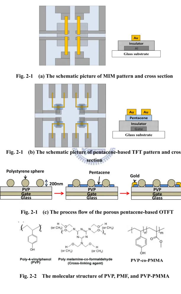
FIG.2-1 (A)THE SCHEMATIC PICTURE OF MIM PATTERN AND CROSS SECTION ... 20
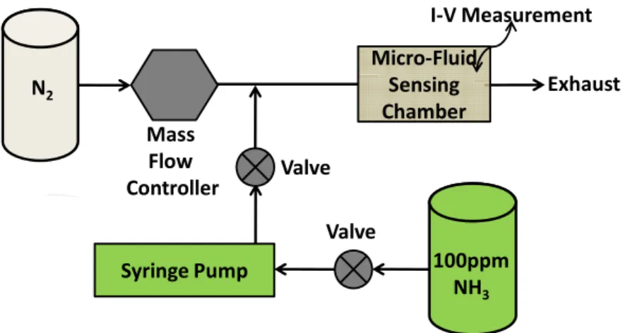
FIG.2-2 THE MOLECULAR STRUCTURE OF PVP,PMF, AND PVP-PMMA ... 20
FIG.2-3MICRO-FLUID SENSING SYSTEM ... 21
FIG.2-4THE PICTURE OF DIGITAL INSTRUMENTS D3100 ... 21
FIG.2-5 THE PICTURE OF CONTACT ANGLE SYSTEM ... 21
FIG.3-1 THE LEAKAGE CURRENT DENSITY OF MIM WITH PVP AND PVP-PMMA DIELECTRICS. ... 31
FIG.3-2 THE CHARACTERISTICS OF PVP AND PVP-PMMAOTFT MEASURED IN AMBIENT. ... 31
FIG.3-3 AFM IMAGE AND SURFACE ROUGHNESS OF (A)PVP(B)PVP-PMMA ... 33
FIG.3-4 WATER CONTACT ANGLE AND SURFACE ENERGY OF (A)PVP(B)PVP-PMMA ... 33
FIG. 3-5 THE TRANSFER CHARACTERISTICS OF (A) PVP OTFT (B) PVP-PMMA OTFT WITH ENCAPSULATION OR NOT ... 34
FIG.3-6 THE TRANSFER CHARACTERISTICS WITH FORWARD AND BACK SCAN OF DEVICES WITH (A)PVP(B) PVP-PMMA IN AMBIENT AIR ... 35
FIG. 3-7 (A) THE LINEAR-REGION TRANSFER CHARACTERISTICS OF DEVICES BEFORE AND AFTER 2000 SECONDS POSITIVE GATE BIAS STRESS (B)THRESHOLD VOLTAGE SHIFT ( VTH) OF PVP AND PVP-PMMA DEVICES DURING POSITIVE GATE BIAS STRESS IN AIR (C) THE LINEAR-REGION TRANSFER CHARACTERISTICS OF DEVICES BEFORE AND AFTER 2000 SECONDS NEGATIVE GATE BIAS STRESS (D) THRESHOLD VOLTAGE SHIFT ( VTH) OF PVP AND PVP-PMMA DEVICES DURING NEGATIVE GATE BIAS STRESS IN AIR ... 37
FIG.3-8 THE TRANSFER CHARACTERISTICS OF DEVICES BEFORE AND AFTER 2000 SECONDS (A) POSITIVE GATE BIAS STRESS (B) NEGATIVE GATE BIAS STRESS ON PVP AND PVP-PMMA DEVICES WITH ENCAPSULATION
... 38 FIG.3-9 THE TRANSFER CHARACTERISTICS OF DEVICES (A) BEFORE AND AFTER 1000, AND 10000 SECONDS UNDER NEGATIVE GATE BIAS STRESS (B) LIGHT ILLUMINATION COMBINED WITH POSITIVE AND NEGATIVE GATE BIAS STRESS ON PVP-PMMAOTFT WITH ENCAPSULATION ... 39
FIG.4-1 (A)AFM IMAGE OF THE PS SPHERE ON THE PENTACENE (B) THE TRANSFER CHARACTERISTICS OF POROUS OTFT IN DIFFERENT ENVIRONMENT (C) POSSIBLE MECHANISM. ... 46
FIG.4-2 SCHEMATIC DEVICE STRUCTURES (A)CONVENTIONAL OTFTS ... 46
FIG.4-3 (A)THE TRANSFER CHARACTERISTICS OF POROUS OTFT IN DIFFERENT ENVIRONMENT (B) THE TRANSFER CHARACTERISTICS TO VARIOUS NH3 CONCENTRATION (C) THE OUTPUT CHARACTERISTICS TO N2 AND NH3 ... 47 FIG.4-4 REAL-TIME MEASUREMENT OF (A) CONVENTIONAL OTFT IS EXPOSED TO 5PPM NH3(B)POROUS OTFT IS EXPOSED TO VARIOUS NH3 ... 48 FIG.4-5POROUS OTFT IS EXPOSED TO 3PPM NH3 IN HUMID N2 ... 49
X
Table Captions
TABLE. 1-1 (A) THE DISEASES AND INGESTIONS ASSOCIATED WITH UNUSUAL BREATH ODORS. (B)THE CONCENTRATION OF THE DISEASES GASES WERE BREATHED BY PATIENTS. ... 10
Chapter 1 Introduction
1-1 An Overview of Pentacene-based Thin Film Transistors
Recently, organic thin-film transistors (OTFTs) have received great attention due to their low-cost and large-area array application. In numerous organic materials, pentacene is promising candidate due to its high hole mobility. Pentacene is made up of five benzene rings as shown in Fig. 1-1.
In previous studies, there are many superior groups to promote the electrical characteristic of pentacene-based thin-film transistors such as field-effect mobility, subthreshold slope, Ion/Ioff , and low operation voltage.
OTFT arrays to drive liquid crystal (LC) [1] [2] or organic light emitting diode (OLED) [3] which showed full-color moving pictures had been demonstrated. These fabrication processes and the handlings of the backplanes should be carried out in ambient air to enable simple inexpensive production. In these reports, OTFTs were encapsulated by passivation layer to avoid exposing to oxygen or moisture in air, and to avoid damage from the subsequent LC or OLED process. However, even when devices are encapsulated or operated in an inert environment, OTFTs are known to suffer from bias stress effect (BSE) that causes significant threshold voltage shift.
1-2 Operation of OTFTs
A thin film transistor is composed of three basic elements: (i) a thin semiconductor film; (ii) an insulating layer; and (iii) three electrodes (source, drain and gate). Fig. 1-2 show two kinds of standard OTFT device structure. Fig. 1-2 (a) is the top-contact device and Fig. 1-2 (b) is the bottom-contact device, respectively. The general
traditional MOSFET are usually operated in inversion mode while the OTFTs are generally operating in accumulation mode.
Since the pentacene is a p-type semiconductor, negative bias is applied on the gate to turn on our OTFTs. The voltage-drop across dielectric causes the energy band bending in the organic semiconductor and additional positive charge carriers will accumulate at the interfaces. The dielectric serves as a capacitance and can store charges. Then we apply a drain bias to drive the accumulated charges from source to drain and from the drain current. The conduction is determined by the field effect mobility (μFE) which represents charges’ driving ability by the electrical field.
In general, we can divide the operation of OTFTs into two regions: linear region and saturation region. If we add gate bias at turn on state, beginning with small drain voltage, OTFTs are operated in linear region, as given drain become larger the drain current will gradually saturate and into saturation region.
Understand how OTFTs normally operate, parameters such as the threshold voltage, field effect mobility can be extracted according to the measured electric characteristic. In addition, how environment effect devices can also be told by analyzing abnormal changing of these parameters.
1-3 Instability of OTFTs Operation
The bias-stress effect in OTFTs had been studied by using different organic active materials or different gate insulators on different device structures [4]. It was found that, for p-type OTFTs under DC stress, positive gate bias stress caused a positively-shifted VT and negative gate bias stress caused a negatively-shifted VT. The BSE was
reversible by removing gate bias or by applying opposite polarity gate bias. Light irradiation also enhanced the reversal process.
Charge trapping, ion migration, charged-state creation and the formation of bound hole pairs (bipolaron) are several proposed mechanisms to explain the BSE [5]. Charge trapping and ion migration were found to be dominant mechanisms in OTFTs with an organic dielectric [6]. When using thermally-grown SiO2 as the gate dielectric to study
OTFTs reliability, charged-state creation is usually believed to be responsible for ΔVT.
John E. Northrup and Michael L. Chabinyc used density functional calculation to simulate defect states generation in pentacene film and found that it was due to the formation of oxygen- and hydrogen-related defects such as C-H2, OH, and C-HOH in
organic semiconductors [7]. Gu et al. also studied the response time of the defect states in pentacene. Long-lifetime deep electron traps were proposed to explain the hysteresis effect in pentacene-based OTFTs [8].
1-4 Defect Generation Mechanism
Until now, device reliability issue has been a greatest barrier to realize the organic electronic application. Even when devices are encapsulated, the threshold voltage (VT)
tends to shift under continuous bias and the field-effect mobility degrades after prolonged storage in normal environment [6]. The device threshold voltage shift (ΔVT)
is generally attributed to hole/electron trapping in the interface between pentacene and dielectric. Although the field-effect mobility degradation mechanism is not clearly understood, the permeation of H2O and O2 in pentacene film is the usually proposed
mechanism. These two phenomena seriously strict the organic TFTs application ranges.
1-5 Threshold Voltage Shift Mechanism
The ΔVT of OTFTs is believed due to the carrier trapping by the defect states.
into two kinds: negative bias stress and positive bias stress.
First, micro process of defect creation under negative bias stress is introduced. The formation of bipolaron proposed by R. A. Street et al. (Phys. Rev. B, vol.68, 085316, 2003) is one of the plausible mechanisms. The deep states slowly trap holes to form bipolarons. The formation of bipolarons would cause the ΔVth due to the reduction of
mobile holes. The reaction can be expressed as: BP
h h+ →( hh )
The other possible mechanism was proposed by John John E. Northrup et al. (Phy. Rev. B, vol.68, 041202, 2003) They studied the formation of hydrogen- and oxygen-related defects (C-H2, OH, and C-HOH) in pentacene film based on the density functional
calculation. The defect creation reactions were given as follows:
and
22 16 22 14 22 15 22 15
2h++C H O C H+ →(C H O)+ +(C H )+
When the pentacene film is in a hole-rich environment, both these two reactions tend react to the right-hand side and produce positive-charged states that cause the ΔVTH.
Either bipolaron formation or hydrogen-, oxygen-related defect creation, these studies need more experimental results to support their theories. Both mechanisms assume that the reaction rate is proportional to the carrier concentration.
However, compare with negative bias stress effect, there are fewer studies focused on positive bias stress effect. Applying a prolonged positive bias to the device usually causes electrons trapping in the channel and a threshold voltage shift forward positive bias. After removing the positive bias, the recovery of trapped electrons can be observed and the device threshold voltage comes back to the original value. Until now, the micro process of electron trap generation under the positive bias stress is not
+
+ + + →2( )
discussed in detail.
1-6 Hysteresis Mechanism
The hysteresis effect is often found in OTFTs, such as polymer gate dielectrics with hydrophilic and polar groups. The large hysteresis prohibits the OTFTs from applying to a circuit and a switch device for active matrix displays. The threshold voltage in the semiconductor accumulation mode is given as [9]:
V qn d
C V
, by this equation we could get a change in VT between forward and backward scan then
cause hysteresis effect we observe, there are three factor could affect the VT change,
1. no changes (due to charge trapping).
2. Ci changes (charge injection form gate into dielectric or slow polarization). 3. Vfb (structural changes in the semiconductor).
Except the reason about above mathematical equations, the hysteresis effect formation can be classified to three general mechanisms [10]:
1. Channel/dielectric interface induced effect
2. Residual dipole-induced effect caused by slow polarization in the bulk organic dielectric
3. The effects of charges injected from gate electrode.
The OTFTs with polymer gate dielectrics might have anyone mechanisms to affect operation stability. Until now, it’s not clearly for saying hysteresis phenomenon for polymer dielectrics how to form and how to influence the device operation such as memory effect and bias stress effect.
1-7 Polymer Gate Dielectrics
Polymer gate dielectrics can offer application such as large area, simple process, and flexible displays. The interface between organic semiconductor and insulator has strongly relation to electric properties like carrier mobility, threshold voltage, and charge trapping.
PVP (Poly (4-vinyl phenol)) has been reported to be the best polymer gate dielectric. Because it offers high mobility, low leakage, cross-link ability [11], and show the potential for photo-pattern possibility [12]. But its stability such as hysteresis and bias stress effect are need to overcome for application of display circuit. The hysteresis is associated with dipole polarization in the dielectric bulk related to gate voltage, charge trapping in the dielectric due to gate inject charge [13]. Recently, several groups investigated hysteresis and bias stress effect problem of pentacene-based TFTs with bilayer gate dielectrics like PVP and SiO2 [13-16]. The
thickness of PVP represents the amount of residual OH group could cause slow polarization induced hysteresis [13]. There have been many attempts to reduce the concentration of hydroxyl groups in the polymer gate dielectrics by cross-linking them with curing agents, both thermally and photochemically [13-17]. The cross-linking agent ration to PVP is also discussed, increase PMF amount would decrease hole mobility and reduce hysteresis effect [17]. By deep curing PVP or in a vacuum chamber could found polarization effect decrease.
PVP-co-PMMA (poly(4-vinyl phenol)-co-(methyl methacrylate)) has been reported to fabricate hysteresis-free pentacene TFT [19]. The polymer dielectric looks like better than PVP, due to its low leakage current, hysteresis-free, high on/off ration, and photo-crosslink ability. But its bias stress effect is not discussed and hydroxyl groups in the polymer how to influence less to the OTFTs.
1-8 OTFTs for Gas-sensing
For the next generation of sensor applications of medical diagnostics, food monitoring, and chemical or biological warfare are desirable. Portable, low cost, and low power-consumption will be newly demands. The OTFTs should be an adequate candidate due to its solubility and simple fabrication process. In recent, OTFTs are proposed to do as gas sensors. When OTFTs exposed to gaseous species, five parameters: turn on current (Ion), turn off current (Ioff), threshold voltage (VT),
field-effect mobility (μFE) and the subthreshold-swing (S.S), are used to estimate the
gas interaction with OTFTs [20].
Analyzing the chemical composition of human breath helps people to examine their health conditions. A breath-testing for alcohol has been used to detect ethanol concentrations in the ppm range since 1960s and it has been applied extensively in alcohol test of car drivers. Except the main components such as nitrogen, oxygen, water vapor and carbon dioxide, more than 200 gaseous molecules (organic or inorganic) (Conkle, J. P. et al, 1975) exist in human breath. These gaseous species produced in human body reflect normal physiological biochemical processes or pathological conditions such as gastric ulcer, liver disease, cancer, or renal failure. Increased concentrations of some species (target analytes) have been found to correlate with certain diseases as listed in Table 1(a). Sensing the unusual concentration of these target analytes in human breath can be a helpful reference to detect human body conditions. In other words, if sensors can be developed to detect and trace these target analytes in patients’ breath, non-invasive diagnostic of above diseases can be realized.
1-9 Gas Sensing Mechanisms for OTFTs
Morphology effect is a critical sensing mechanism, it could decide gaseous diffuse into channel quickly or slowly. Grain boundaries play an important role in OTFT sensing. The grain size was varied by changing the substrate temperature during deposition, deposition rate surface roughness, and surface energy of dielectrics.
In the organic semiconductor, both grains and grain boundaries could be affected by the analyte. Due to their dipole, the analyte molecules bound on grain boundaries will trap the mobile charge carriers from channels.[21-22] Meanwhile the analyte interacting with the semiconductor grains will result in excess holes through chemical processes that are not completely understood.
1-10 OTFTs for Ammonia Gas Sensing
According to medical reports (C. Shimamoto et al, 2000), breath ammonia levels are significantly higher in cirrhotic patients (0.745 ppm) than in controls (0.278 ppm). Ammonia is an important index for uremia and chronic liver disease as listed in Table 1(b).Patients who have renal failure even exhale 4.8 ppm ammonia in their breath. Current ammonia sensors such as polyaniline sensors, metal oxide sensors, catalytic sensors, and optical analyzers have disadvantages such as high operation temperature, low sensitivity or high cost (G.K. Prasad et al., 2005; Björn Timmer et al., 2005). OTFT is promising to be a non-invasive, inexpensive, portable and disposable diagnostic device because of its low cost fabrication process and high sensitivity to gas molecules.
1-11 Motivation
Organic thin-film transistors (OTFTs) have been extensively explored due to their potentials for low-end electronic applications: drivers for flexible displays, complementary circuits, and radio-frequency identificationtags (RFID). PVP is a well-known polymer gate dielectric due to low leakage and high carrier mobility, but owing to hydroxyl group results in worse bias stress effect and hysteresis show. Make it’s hard to apply for flexible display driving, etc. On the contrary, there is less gate bias stress effect and hysteresis-free for OTFT with PVP-PMMA dielectric which also has hydroxyl group. In previous work, the cross-linking agent ration to PVP is also discussed, increase PMF amount would decrease hole mobility and reduce hysteresis effect [17]. There is high hole mobility for OTFTs with PVP dielectric might due to hydroxyl group dominating. But hydroxyl groups influence on PVP and PVP-PMMA devices differently in ambient air. Above all, it’s necessary to realize polymer dielectrics with hydroxyl groups how to influence OTFTs operation in ambient air.
In this thesis, we infer hydroxyl groups of PVP dielectric absorb much water vapor, and enhance extra holes in channel due to electron traps formation with dielectric surface and water vapor. Further, in order to make sure moisture could significantly affect OTFTs operation due to hydroxyl group charging. We fabricate a novel porous OTFT for water vapor could rapidly pass in and out PVP surface. It is reported that breath NH3 concentration is higher in cirrhotic patients (0.745
ppm) than that in normal person (0.278ppm). OTFTs as NH3 gas sensors were reported to have sensitivity in the low-ppm levels. In this thesis, electron interactions rapidly with ammonia gas molecules and dielectric surface induce extra carrier in the channel by the porous structure. A novel ammonia gas sensor is demonstrated to realize a
Fi Ta B D (a) (b) L ig. 1-2 OTF ble. 1-1 (a) (b)The c Breath comp disease m Aceton Ammon Butyric a Ethaneth Hydrogen Disease Gas Renal failur ) Liver Cirrho Fig. 1-1 FT device c ) The diseas concentrati ponent as a marker ne nia acid hiol n sulfide re sis Pat
Figure
1 The mole configuratioses and ing ion of the d Dia Uremia; C Liv Liv Pe 4. Am tients ≥ 0.745
s of Ch
ecular struc on: (a)Top-gestions ass diseases gas Diseases betes; lung c Chronic live ver Cirrhosi ver Cirrhosi riodontal dis .8ppm mmonia 5ppm ; healtapter 1
cture of pen -contact de ociated wit ses were br cancer er disease is is sease th ≤ 0.278pp ntacene evice (b) Bo th unusual reathed by Refe Ebeler e Grote et Davies e Manosis Manosis Manosis Manosis Da Ref Shim m ottom-conta breath odo patients. rences et al., 1997 t al., 1997 et al., 1997 s., 1983 s., 1983 s., 1983 s., 1983 avies, 1997 ferences mamoto, 2000 act ors. 0Chapter 2 Experimental Setup
2-1 Introduction
The structures are made the Metal-Insulator-Metal (MIM), top-contact bottom-gate Thin Film Transistors (TFTs), and a novel porous structure of pentacene-based TFT. We will introduce our devices how to fabricate, and the pattern of devices is shown in the Fig. 2-1 we use in this thesis. And the parameter of device extracting method and material analysis we use.
2-2 Cleaning the Glass Substrate
There are two steps to clean and remove particle and organic pollution on Glass substrate (CORNING EAGLE 2000). The roughness of glass substrate is important for metal deposition and metal adhesion, or could cause point defect to influence the interface between organic layer and metal.
The glass cleaning steps are as follow: Steps:
(1) Glass substrates are place of the DI water current flow for 5 minutes in order to remove the particles.
(2) Put the glass substrates in the acetone with ultrasonic resonance for 5minutes to remove the organic pollution
(3) Put the glass substrates under the DI water current flow for 5 minutes to remove the solvent.
(5) Put the glass substrates under the DI water with ultrasonic resonance for 1 minute twice to remove the residual solvent.
(6) Dry the glass substrates with N2 flow to blow off the water drop on the
substrates
(7) Put the glass substrates on the hot plate at 120℃ for 3 minutes to remove the moisture.
(8) Naturally cool down to the room temperature.
2-3 Metal-Insulator-Metal Fabrication
2-3.1 Bottom Metal Deposition
Before metal deposition, the glass substrates should be cleaned. The 50 nm Aluminum (99.999%) was deposited by thermal evaporator around 5x10⁻⁶torr. The deposition rate was controlled at 2Å/sec and substrate heater was hold at 60℃, the adequate deposition rate and temperature were benefited to help metal film have good adhesion to glass substrate. The metal pattern was defined by shadow mask.
2-3.2 Dielectric Fabrication
In this section, introduce each of the dielectric layer deposition respectively: 1. Poly (4-vinyl phenol) (PVP):
PVP was obtained from Aldrich with molecular weight about 20000. PVP have OH function groups on its molecule structure, poly(melamine-co-formaldehyde) (PMF) was used to be cross-linking agent for PVP, and propylene glycol monomethyl ether acetate (PGMEA) as the solvent. Their chemical structures of PVP and PMF are schematically shown in Fig. 2-2. First, we dissolved PVP and PMF in the PGMEA solvent with a magnetic stirrer for overnight. PVP was 8wt% in the solution, and fixed
PVP and PMF weight ratio was 11:4. We then filtered mixed solution through a syringe filter with 0.2μm PTFE membrane and spin coating on the substrate at 1200 rpm for 1min. To avoid metal pad or bonding result in unnecessary leakage current through the insulator, we removed additional solution on the substrate by the cotton swabs with PGMEA. Put the substrates on the hot plate and cured at 200℃ for 1 hour in the ambient air. The cross-link reaction was more completed at high temperature and for a long time, let OH functional groups on the PVP can be cross-linked by PMF as more as possible.
2. Poly(4-vinyl phenol-co-methyl methacrylate) (PVP-PMMA):
PVP-PMMA was obtained from Aldrich, PVP-PMMA copolymer both have phenol and methyl methacryl functional group chain. The chemical structure of PVP-PMMA is schematically shown in Fig. 2-2. We dissolved 15wt% PVP-PMMA in the N, N-dimethyl formamide (DMF) and put the solution on the hot plate at 70℃ until spin-casting the solution on the substrate. After spin coating of the polymer solution, to avoid metal pad or bonding result in unnecessary leakage current through the insulator, we removed additional solution on the substrate by the cotton swabs with DMF. The polymer film was baked on the hot plate at 150℃ for 1 hour. Because PVP-PMMA solution didn’t mix cross-linking agent, the film could be removed easily by acetone, ethanol, etc.
2-3.3 Top Metal Deposition
We deposited Gold (99.999%) as the top metal on the film. The deposition was started at 5×10⁻⁶torr and rate was controlled at 1Å/s. Au electrodes are defined through shadow mask and orthogonal to bottom metal. The destination of gold evaporation was used to simulate the actual structure for source/drain & gate metals of pentacene TFT.
2-4 Pentacene-based Thin Film Transistors Fabrication
2-4.1 Bottom Gate Metal Deposition
Before gate metal deposition, the glass substrate should be cleaned. The 50-nm Aluminum (99.999%) was deposited by thermal evaporator around 5x10⁻⁶torr. The deposition rate was controlled at 2Å/sec at 60℃.The gate metal pattern and metal pad were defined by shadow mask. The width of gate metal pattern was set up to be 1.5mm. The device has large contact resistance if the width of gate metal is less than channel length.
2-4.2 Dielectric Film Formation
After gate metals defined, we purged the N2 flow to keep the substrates clean. The
solutions of PVP and PVP-PMMA were spin coating on the different substrates. Similarly, we removed additional solution by the cotton swabs with PGMEA and DMF. And put each other on the hot plates in the ambient air. (PVP at 200°C and PVP-PMMA at 150°C for 1 hour).
2-4.3 Pentacene Thin Film Growth
The pentacene material obtained from Aldrich without any purification. Put the substrates with PVP and PVP-PMMA dielectric into the thermal evaporator until high vacuum pressure (3x10⁻⁶torr), we evaporate 50-nm-thick pentacene film. The deposition rate of pentacene was controlled at 0.4~0.5Å/sec at room temperature and active layer was defined by shadow mask.
2-4.4 Source and Drain Electrodes Deposition
We deposited 70-nm-Au (99.999%) through shadow mask as source and drain electrodes of pentacene-based TFTs. The deposition was started at 5×10⁻⁶torr and rate was controlled at 1Å/s. The device channel width and length was 1000μm and 200μm. We can get conventional top contact and bottom gate TFT schematic as Fig. 2-1 (b)
2-5 Encapsulation of Pentacene-based TFT in Anhydrous
Oxygen Environment
When the devices have been fabricated, the devices are got from the vacuum chamber to the ambient air. We first investigate their characteristic under the ambient environment and the relative humidity is about 65%. Then we do encapsulation for the devices, action in the glove box which environment is filled with nitrogen and ultra low water vapor and oxygen (H2O<0.1ppm, O2<0.1ppm). Put the samples into glove box
and send to vacuum chamber linked to glove box. By the turbo pump, the device is under 1×10⁻⁶torr (ultra high vacuum) to make sure the water vapor absorption have been excluded. Then take it out in the glove box and use UV binder to joint substrates and package glass under UV light exposure in one minute. As a result, the OTFTs are situated in anhydrous oxygen environment with encapsulation can be measured by wire bonding and metal pad, even though the devices are encapsulated with package glass isolation.
2-6 A Novel Porous Structure of Pentacene-based TFT
under high vacuum (5x10⁻⁶torr) deposit 50-nm-Al (99.999%) film as the bottom gate metals and defined by shadow mask. We mixed the polymer dielectric solution as of 8%PVP (PVP: PMF =11:4) with PGMEA. The dielectric layer of OTFT devices is spinning on the gate metal and bake at 200℃ 1 hour under ambient air. The thickness is measured to be 420nm by Alpha-step. After cross-link reaction is completed. We put the glass substrates exposed to UV/Ozone in 5 seconds to increase PVP surface polarity for enhancing sensitivity for NH3.
The next step is to fabricate nano-scale meshed pentacene structure. We use high density polystyrene spheres as shadow mask. Positively charged polystyrene particles (200 nm, tetra-methylammonium latex) were adsorbed onto the substrates from dispersion by electrostatic interactions. Particles concentration was diluted with ethanol to 0.8 wt%. Immersion time was 3 minutes to allow the adsorption to reach saturation. Excess particles were rinsed off in a beaker with ethanol and then transferred to a beaker with boiling isopropanol(IPA) solution for ten seconds. The key procedure in this fabrication is that the substrate is then transferred to a beaker with boiling isopropanol solution for ten seconds. The substrate is finally blown dry immediately in a unidirectional nitrogen flow. The benefit of this method is the possibility to process large areas in a short processing time without photolithography.
Then under high vacuum (3×10⁻⁶torr) deposit 50-nm-pentacene thin film as active layer and defined by shadow mask. We deposited 100-nm-Au (99.999%) through shadow mask as source and drain electrodes of pentacene TFT. The deposition was started at 5×10⁻⁶torr and rate was controlled at 1Å/s. The device channel width and length was 1000μm and 200μm. The process flow of the porous pentacene-based OTFT and schematic diagram are shown in Fig. 2-1 (c).
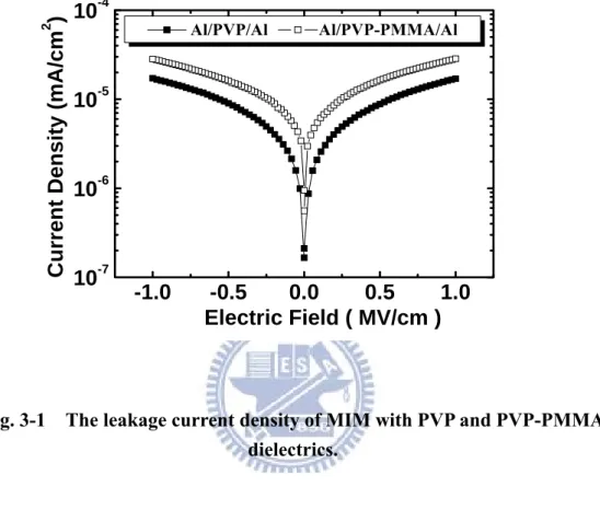
2-7 Micro-Fluid Gas Sensing System
As shown in Fig. 5, various NH3 concentration is obtained by uniformly mixing
various amount of NH3 (from a cylinder contains 100 ppm NH3) with high purity
nitrogen (N2) into a 20-cm-long U-shape tube. The amount of N2 is controlled by a
mass-flow controller. The amount of 100 ppm NH3 is controlled by an electrical
syringe pump. The U-shape tube with mixed gas is connected to a micro-fluid measuring system made by Polytetrafluoroethylene (PTFE) (width = 1 cm, length = 3.5 cm, and height = 0.1 cm). Two Keithley 2400s are utilized to synchronously generate -5 V (drain terminal) and 30V (gate terminal) pulse each 50 millisecond and read out the currents
2-8 Devices Electrical Parameter Extraction
Field effect mobility, threshold voltage, subthreshold slope and Ion/Ioff ratio are
usual used to compare different devices’ performance. In the following section, extraction methods would present how to extract parameters from electrical transfer characteristic of pentacene.
2-8.1 Field Effect Mobility (μ
FE)
The field effect mobility (μFE) was determined by the orientation of pentacene
molecules near gate dielectric. Therefore, gate dielectric surface states strongly affect the device μFE. The device μFE variation can be used to compare the difference between
PVP and PVP-PMMA dielectric layers. In our experiment, μFE were extracted by using
transistor and can be expressed as
I - Saturation region
, where Ceff and VT are effective capacitance per unit area and the threshold voltage. W
and L are device channel width and channel length. When operating device at low drain bias, the linear region equation can be modified to
I - Linear region
Generally, mobility can be extracted from the transconductance maximum GM in the
linear region:
The field effect mobility can be extracted from the transconductance and this equation can be expressed as
In this study, we used max GM value to calculate and define the field effect mobility.
2-8.2 Threshold voltage (V
T)
Threshold voltage (VT) determines the device operation voltage and smaller VT
can help to lower power consumption. Because VT strongly dependents on dielectric
surface states, environmental and fabrication process variations easily cause a shift on the VT. Based on this phenomenon, the device VT shift is usually used as an importance
parameter when pentacene-based TFTs applied to photo-detector or biochemical detector. In this study, we used the linear region equation to extract the device VT.
2-9 Material Analysis Instruments
2-9.1 Atomic Force Microscope (AFM)
Since PVP treated surface may exist OH groups, its surface morphology can also be different compare with PMMA surface. In addition, pentacene deposits on PVP (hydrophilic) and PMMA (hydrophobic) influenced by these two kinds of surfaces may have different grain size or morphology, too. Atomic force microscope (AFM) is used to measure surface morphology on a scale from angstroms to 30 microns. It scans samples through a probe or tip, with radius about 20 nm. The tip is held several nanometers above the surface and using feedback mechanism that measured interactions between tip and surface on the scale of nanoNewtons. Variations in tip height are recorded when the tip is scanned repeatedly across the sample, then producing morphology image of the surface. In this experiment, the used equipment is Digital Instruments D3100 as shown in Fig. 2-3 and the used active mode is tapping mode.
2-9.2 Contact Angle System
Contact angle system is used to estimate wetting ability of a localized region on a solid surface. The angle between the baseline of the drop and drop boundary is measured. Comparing the result can tell the material surface is relatively hydrophilic or hydrophobic, then can further analysis surface chemical composition. Since PVP have OH groups on its molecular structure while PVP-PMMA have less. We prepared the glass substrate coating with PVP and PVP-PMMA. By the contact angle system, we found the water contact angle and surface energy of PVP and PVP-PMMA were similar.
Figure of Chapter 2
Fig. 2-1 (a) The schematic picture of MIM pattern and cross section
Fig. 2-1 (b) The schematic picture of pentacene-based TFT pattern and cross section
Fig. 2-1 (c) The process flow of the porous pentacene-based OTFT
Fig. 2-2 The molecular structure of PVP, PMF, and PVP-PMMA Glass substrate Al Insulator Au Glass substrate Gate Insulator Pentacene Au Au Glass PVP Gate Gold Glass PVP Gate Pentacene Glass PVP Gate Polystyrene sphere 200nm PVP-co-PMMA
Fig. 2-3 Micro-fluid sensing system
Fig. 2-4 The picture of Digital Instruments D3100
Fig. 2-5 The picture of contact angle system
N2 100ppm NH3 Mass Flow Controller Syringe Pump Micro‐Fluid Sensing Chamber Exhaust Valve Valve I‐V Measurement
Chapter 3 Result and Discussion
3-1 Metal-Insulator-Metal Leakage Test
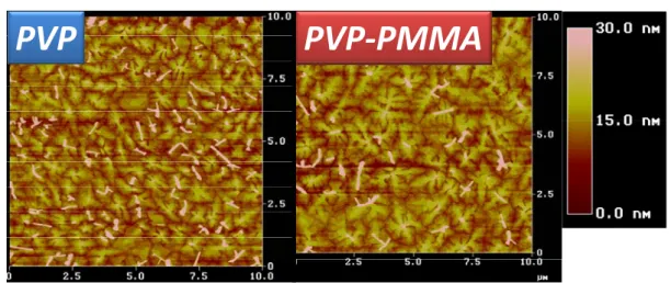
Follow previous sections, we can get two polymer dielectric between Al and Au electrodes, and the cross-section were 1×1 mm2. The thickness of the polymer films measured by using a surface profiler (Alpha-step) was about 420nm. So we can investigate the electrical insulating properties and capacitance of PVP and PVP-PMMA. We applied one electrode voltage sweep from 0 to ±50v and the other electrode was ground. Fig. 3-1 showed the MIM leakage current density were 1.71×10⁻⁸ A/cm2 and 2.85×10⁻⁸ A/cm2 in an electric field of 1MV/cm. Showing that PVP and PVP-PMMA both have enough insulating properties for OTFT operation. The measured capacitance of the MIM structure with PVP and PVP-PMMA was approximately 8.8nF/cm2 and 5.6nF/cm2.
3-2 Characteristics of Pentacene-based TFTs with PVP and
PVP-PMMA Dielectrics
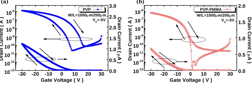
Electrical transfer characteristics of pentacene-based organic thin film transistors (OTFTs) with PVP and PVP-PMMA dielectrics measured in the ambient air and in the dark are shown in the Fig 3-2. We operated the device in the linear region |VD| |VG VT| and got field effect mobility (μFE) and threshold voltage by extracting from
transfer of characteristics devices. The μFE and VT of PVP OTFTs were about
0.5~0.6cm2/Vs and -15 V. And the μFE and VT of PVP-PMMA-OTFTs were close to
PVP-PMMA was 3×10⁵. In our research, if we measured transfer characteristics (ID-VG)
more times, we could know threshold voltage of PVP OTFT easily shift to positive, but PVP-PMMA OTFT was much more stable only shift less. Apparently, PVP-PMMA OTFT has fine characteristics for display application than PVP OTFT. In the next sections, we would explain why the PVP OTFT has higher mobility but poor stability than PVP-PMMA OTFT.
3-3 Morphology of PVP, PVP-PMMA and Pentacene Thin
Films
Before and after depositing pentacene thin films on organic gate dielectrics, using atomic force microscope (AFM) to observe the morphology of PVP, PVP-PMMA and pentacene films deposited on PVP and PVP-PMMA. Surface roughness is one of factors that can effect semiconductor crystallization. Pentacene grow on smooth surface usually have better morphology and mobility than grow on rough surface. Fig. 3-3(a) and (b) are atomic microscopy images of PVP and PVP-PMMA gate dielectric before depositing pentacene thin films. Both PVP and PVP-PMMA have smooth surface roughness about 0.5 nm. Fig. 3-3 (c) and (d) are atomic microscopy images of pentacene thin films on PVP and PVP-PMMA gate dielectrics. By telling (c) and (d) images, pentacene films have similar grain size no matter it was deposited on PVP or PVP-PMMA surface. However, according to the study proposed by Sangyun Lee et al, OH-terminated interface may increase the mobility by supplying the hopping sites, the carriers then can move easily through the channel. Fig. 3-3 (e) show the AFM images of pentacene films morphology during
PVP-PMMA rather than PVP. It is reported the large grain size of pentacene-based TFTs on the much hydrophobic surface have higher mobility is observed during initial pentacene film growth state [23]. In our experiments, OH groups’ effects on OTFTs need further experiment to study why the PVP-PMMA OTFT also have OH group but not present high mobility like PVP OTFT.
3-4 Wet-ability of PVP and PVP-PMMA Dielectrics
PVP and PVP-PMMA films were fabricated by using spin-coating process on the glass substrates. Water contact angles of PVP and PVP-PMMA dielectric surfaces were 67.3o and 63.9o as shown in Fig. 3-4 (a) and (b). Previous researches mentioned that water contact angle strongly dependents the chemical composition of dielectric surface. Fig. 3-4 (a) and (b)shows that PVP dielectric surface has indistinct difference with PVP-PMMA because OH groups also consist in PVP and PVP-PMMA molecule structure. But they also provide a good surface energy for pentacene deposition. Surface energy of PVP and PVP-PMMA calculated were 50.3 mJ/m2 and 48.3 mJ/m2.
3-5 Moisture Effect on OTFTs Operation
Of the polymer gate dielectrics reported in the literature, PVP is perhaps the dielectric with the highest mobility for pentacene-based TFTs. We try to clarify why PVP-OTFT has higher mobility than PVP-PMMA OTFT. In our work, we do encapsulation in the anhydrous oxygen environment for PVP OTFT and PVP-PMMA OTFT. Fig. 3-5(a) and (b) show the transfer characteristics of OTFTs with or w/o encapsulation. By the Table 2, we can get information of moisture effect to OTFTs. PVP OTFT with encapsulation has the lowest mobility and the lowest threshold voltage
in the Table 2. We can infer the moisture contributes large mobility to PVP OTFT, because OH groups closed to the channel easily interact with water vapor to become electron traps to induce extra hole. In contrast, the mobility of PVP-PMMA OTFT has less change. It means the methyl methacryl groups not only prevent moisture invade but also perform good behavior for OTFTs such as stable electrical properties, high on/off ratio, low leakage current.
3-6 Moisture Effect on Hysteresis Phenomenon Investigation
Though PVP OTFT have high mobility than PVP-PMMA OTFT in ambient air, but its instability has been widely discussed in previous researches [13-17], hysteresis and bias stress effect were observed in the transfer characteristic of pentacene-based TFTs with PVP dielectric. In this section, we firstly discuss the hysteresis of PVP-OTFT and PVP-PMMA-OTFT in ambient air, and then we encapsulate two devices to observe the hysteresis phenomenon in anhydrous oxygen environment.
3-6.1 Hysteresis Phenomenon Investigation on OTFTs in
Ambient Air
Devices with PVP and PVP-PMMA dielectrics were prepared to measure by semiconductor parameter analyzers HP4156A (Agilent). Every time we fabricated the device completely and vacuumed them in boxing quickly to prevent moisture intrusion. First, we measured them in the dark box in the ambient air with a relative humidity of 65% at room temperature 25°C. We given symmetric sweeps from VG=+30V to
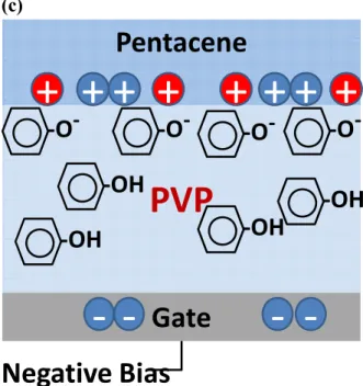
electrical transfer characteristics of devices. We observed hysteresis behavior appeared for the PVP-OTFT, but no hysteresis was observed for the PVP-PMMA OTFT. It was found that back scan current (on to off) was large than forward scan current (off to on) (or called clockwise hysteresis), it’s different with hysteresis due to hole trapping in the channel/dielectric interface [14]. But it is considered to relate with residual dipole-induced effect caused by slow polarization in the bulk organic dielectric with hydroxyl groups. This behavior is often found in the PVP or terminated-OH (hydroxyl groups) dielectric, which can be slowly reoriented by an applied electric field [5]. When PVP OTFT swept from off to on, extra hole would be stay in the channel/dielectric interface. Then we sweep gate voltage from on to off mode, the extra hole can’t be released rapidly by slow polarization due to dipole reorientation. That is why back scan current is large than forward scan current, so the hysteresis is formed. Respect to PVP-PMMA-OTFT, no hysteresis is observed in the on and subthreshold swing region. Hydroxyl groups in PVP-PMMA might difficultly be charged or be interfered the polarity of vinyl phenol by MMA groups. It seems that PVP-PMMA OTFT has no memory effect on device operation.
3-6.2 Hysteresis Phenomenon Investigation on OTFTs with
Encapsulation
In previous section, we find PVP OTFT has hysteresis but PVP-PMMA OTFT has hysteresis-free in dark and ambient environment. Although PVP and PVP-PMMA dielectrics both have OH groups, the hysteresis phenomenon is not found for the PVP-PMMA OTFT. In previous researches [5], water vapor might diffuse to PVP bulk dielectric results in slow polarization when OTFT operates. We try to investigate water vapor how to influence two devices both have OH groups. Put devices in the anhydrous
glove box after achieve high vacuum pressure in the chamber, and then encapsulate the devices in the anhydrous oxygen glove box. Also give symmetric sweeps from VG=+30V to VG=-30V (off to on) and back scan from VG=-30V to VG=+30V (on to off)
and VD=-5V, VS=0V. Fig. 3-6 (c) and (d) are electrical transfer characteristics of
devices. Both OTFTs with PVP and PVP-PMMA are hysteresis-free after encapsulating the devices in the anhydrous oxygen environment. It is clearly saying that hysteresis behavior due to water vapor for PVP-OTFT. The amount of OH groups would increase water vapor absorption in the bulk dielectric. As PVP-OTFT in the anhydrous oxygen environment, no water vapor absorption results in slow polarization. On the contrary, PVP-PMMA-OTFT shows hysteresis-free even in ambient air, so we guess the MMA group is much hydrophobic for moisture that made water vapor is difficult to invade dielectric bulk.
3-7 Bias Stress Effect on OTFTs in Ambient/Anhydrous
Oxygen Environment
As above description, pentacene thin film deposited on organic dielectrics with PVP and PVP-PMMA groups had different interface states between gate dielectric and pentacene thin film owing to grain size of pentacene initial growth state. In this section, we discuss the OH group influence on the device reliability, and the defect generation mechanism. However, one of main degradation mechanisms is OH group exists and interacts with water vapor.
3-7.1 Bias Stress Effect on OTFTs in Ambient Air
In this section, the bias stress effect on devices with PVP and PVP-PMMA groups in the dark and ambient air environment was discussed. Because Au/pentacene contact barrier is prefer to hole transportation, pentacene-based TFTs in this study is p-type. The positive gate bias was applied to stress the device at off-state region and the negative gate bias was applied to stress the device at on-state region.
For positive gate-bias stress, VG was kept at +15 V and VD = VS were 0 V for 2000
sec. The linear-region transfer characteristics of devices before stress and after 2000-sec stress are depicted in Fig. 3-7 (a). Then, threshold voltage shift (△VT) curves
of devices with PVP and PVP-PMMA gate dielectrics were plotted as a function of bias stress time as shown in Fig. 3-7 (b). We found that positive gate-bias stress influences on devices with PVP and PVP-PMMA gate dielectrics were similar but different with pentacene-based TFT on SiO2 dielectric [8]. Obviously, the gate-bias stress causes a negative shift of the transfer characteristics of devices with PVP and PVP-PMMA gate dielectric. For the negative gate-bias stress, VG was kept at -15V
minus initial threshold voltage (-15V-VT) while VD = VS were 0 V for 2000 sec. The
linear-region transfer characteristics of devices before stress and after 2000-sec stress are depicted in Fig. 3-7 (c). Then, threshold voltage shift (△VT) curves of devices with
PVP and PVP-PMMA gate dielectrics were plotted as a function of bias stress time as shown in Fig. 3-7 (d). The negative bias stress caused a △VT of both transfer
characteristics of device with PVP and PVP-PMMA gate dielectrics. The △Vth of
device with PVP gate dielectric is much larger than with PVP-PMMA gate dielectric, even make device situate normally on-state. Compare to the positive gate bias stress, the negative gate bias stress caused large △Vth of device with PVP-PMMA dielectric.
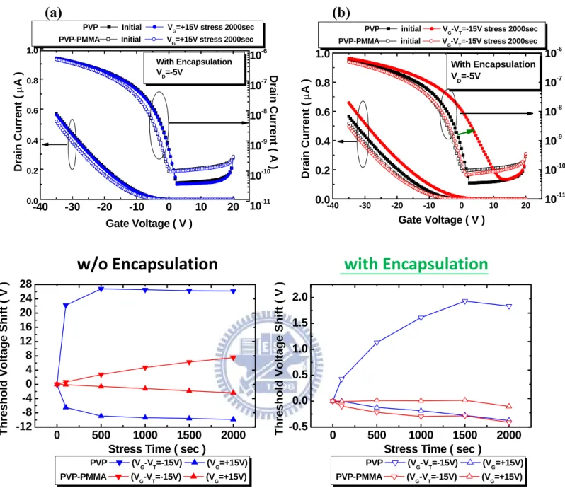
3-7.2 Bias Stress Effect on OTFTs with Encapsulation
After discuss pentacene-based TFTs in ambient air, we encapsulate the devices with PVP and PVP-PMMA dielectrics and measure the same gate-bias stress condition like previous section. For positive gate-bias stress, the transfer characteristics of both devices are depicted in Fig. 3-8 (a). Both transfer characteristics of devices keep almost unchanged after applied VG=+15V stress 2000-seconds. Apparently, polymer
dielectrics with OH groups in anhydrous ambient hardly form electron traps with water vapor.
For negative gate-bias stress, the transfer characteristics of both devices are depicted in Fig. 3-8 (b). PVP OTFT still was suffered for negative gate bias stress, but transfer characteristics of PVP-PMMA OTFT almost keep unchanged. It’s a incredible result for stressing device hold on high carrier concentration in the channel. For OTFTs with or without encapsulation, comparison to threshold voltage shift is shown in Fig. 3-8 (c) and (d).
3-8 Superior Stability of PVP-PMMA OTFTs with
Encapsulation
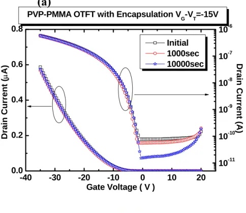
In the last part, negative gate bias stress effect on PVP-PMMA OTFTs with encapsulation has been decreased drastically. Even give voltage -30volts (VG-VT=-15volts) bias stress ten thousand seconds to gate electrode on PVP-PMMA
devices with encapsulation maintain initial electrical properties. Gate bias stress on the transfer characteristics of device are depicted in Fig. 3-9 (a) shows high stability for PVP-PMMA OTFTs. It might be caused in no water environment which OH group is hard to form negative-chareged with water vapor. Further, we use LED backlight to
characteristics with 1.2mW white light illumination as shown is shown in Fig. 3-9 (b). PVP-PMMA device is much more stable with light. Even give gate bias stress on device companied with 1.2mW light. The threshold voltage slightly shifted. Its high stability saying that OH group is too difficult to form negative-charge with water vapor to be electron traps.The similar result is reported for high stability use Cytop [24] as gate dielectric owing to its ultralow gate leakage current.
Figures of Chapter 3
Fig. 3-1 The leakage current density of MIM with PVP and PVP-PMMA dielectrics. -1.0 -0.5 0.0 0.5 1.0 10-7 10-6 10-5 10-4 Al/PVP/Al Al/PVP-PMMA/Al
Current Density (mA/cm
2 ) Electric Field ( MV/cm ) -40 -30 -20 -10 0 10 20 0.0 0.5 1.0 1.5 2.0 2.5 3.0 Drain Current ( A ) V D=-5 V W/L=5 Drain Current ( μ A ) Gate Voltage ( V ) PVP OTFT PVP-PMMA OTFT 10-12 10-11 10-10 10-9 10-8 10-7 10-6
Table. 3-1 OTFT Parameters
Dielectric PVP PVP-PMMA
Ci(nF/cm2) 8.8 5.6
Mobility (cm2/V*s) 0.5~0.6 0.31
Threshold Voltage (V) About -15 About - 14 V
Ion/Ioff Near 5×10⁴ >5×10⁵
PVP
Roughness Rms:5.2A
PVP‐PMMA
Roughness Rms:5.6A
(a) (b)PVP
PVP‐PMMA
(c) (d)Fig. 3-3 AFM image and surface roughness of (a) PVP (b) PVP-PMMA AFM image of 50-nm pentacene on (c) PVP (d) PVP-PMMA
AFM image of 5-nm pentacene on(e) PVP and PVP-PMMA
Fig. 3-4 Water contact angle and surface energy of (a) PVP (b) PVP-PMMA
PVP
PVP‐PMMA
(e) PVP Water contact angle 67.32° Surface Energy 50.3 mJ/m2 PVP‐PMMA Water contact angle 63.96 ° Surface Energy 48.3mJ/m2(a)
(b)
Fig. 3-5 The transfer characteristics of (a) PVP OTFT (b) PVP-PMMA OTFT with encapsulation or not
-40
-30
-20
-10
0
10
20
10
-1210
-1110
-1010
-910
-810
-710
-6Drain
Curren
t (
μ
A )
Drai
n Current ( A )
Gate Voltage ( V )
PVP OTFT w/o encapsulation with encapsulation0.0
0.4
0.8
1.2
1.6
2.0
-40
-30
-20
-10
0
10
20
10
-1210
-1110
-1010
-910
-810
-710
-6Drai
n Cu
rre
n
t (
μ
A )
Drai
n
Current
( A )
Gate Voltage ( V )
0.0
0.4
0.8
1.2
1.6
2.0
PVP-PMMA OTFT w/o encapsulation with encapsulationFig. 3-6 The transfer characteristics with forward and back scan of devices with (a) PVP (b) PVP-PMMA in ambient air
(c) PVP (d) PVP-PMMA with encapsulation
-30 -20 -10 0 10 20 30 10-13 10-12 10-11 10-10 10-9 10-8 10-7 10-6 PVP-PMMA W/L=1000μm/200μm VD=-5V Gate Voltage ( V ) 0.0 0.5 1.0 1.5 2.0 Dr ain Curr ent ( μ A ) Drain Cu rren t ( A ) -30 -20 -10 0 10 20 30 10-13 10-12 10-11 10-10 10-9 10-8 10-7 10-6 W/L=1000PVP μm/200μm VD=-5V Gate Voltage ( V ) 0.0 0.5 1.0 1.5 2.0 2.5 3.0 Dr ain Curr ent ( μ A ) Drain Cu rren t ( A )
(a)
(b)
(a) (b) -30 -20 -10 0 10 20 30 10-13 10-12 10-11 10-10 10-9 10-8 10-7 10-6 PVP-PMMA W/L=1000μm/200μm VD=-5Vw/o encapsulation with encapsulation
Gate Voltage ( V ) 0.0 0.5 1.0 1.5 2.0 Dr ai n Cur rent ( μ A ) Drain Curre n t ( A ) -30 -20 -10 0 10 20 30 10-13 10-12 10-11 10-10 10-9 10-8 10-7 10-6 W/L=1000PVP μm/200μm VD=-5V
w/o encapsulation with encapsulation
Gate Voltage ( V ) 0.0 0.5 1.0 1.5 2.0 2.5 3.0 Dr ai n Cur rent ( μ A ) Drain Cu rren t ( A )
-40 -30 -20 -10 0 10 20 10-13 10-12 10-11 10-10 10-9 10-8 10-7 10-6 Dr ain C u rr e nt ( A ) Gate Voltage ( V )
PVP Initial VG=+15V stress 2000sec PVP-PMMA Initial VG=+15V stress 2000sec
Stress in ambient air
VD=-5V (a) 0 500 1000 1500 2000 -10 -8 -6 -4 -2 0 Δ VTH ( V )
Stress Time ( sec )
A- PVP VG=+5 VG=+10 VG=+15 PVP-PMMA VG=+5 VG=+10 VG=+15 (b) -40 -30 -20 -10 0 10 20 10-12 10-11 10-10 10-9 10-8 10-7 10-6 10-5 Dr ai n Curr ent ( A ) Gate Voltage ( V )
PVP initial VG-VT=-15V stress 2000sec
PVP-PMMA initial VG-VT=-15V stress 2000sec
Stress in ambient air VD=-5V
(c)
0 500 1000 1500 2000 0 5 10 15 20 25 30 A- PVP VG-VT=-5V VG-VT=-10V VG-VT=-15V PVP-PMMA VG-VT=-5V VG-VT=-10V VG-VT=-15V Δ VTH ( V )Stress Time ( sec )
Fig. 3-7 (a) The transfer characteristics of devices before and after 2000 seconds positive gate bias stress (b) Threshold voltage shift (△Vth) of PVP and
PVP-PMMA devices during positive gate bias stress in air (c) The transfer characteristics of devices before and after 2000 seconds negative gate bias stress
(d) Threshold voltage shift (△Vth) of PVP and PVP-PMMA devices during
negative gate bias stress in air
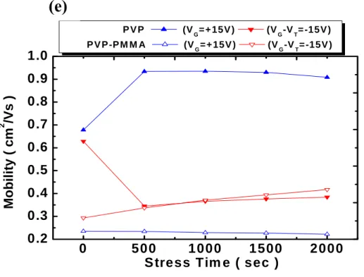
(e) The field-effect mobility plotted as a function of stress time for positive bias and negative bias on the PVP and PVP-PMMA devices
0 500 1000 1500 2000 0.2 0.3 0.4 0.5 0.6 0.7 0.8 0.9 1.0 Mob ilit y ( c m 2 /Vs )
S tress Tim e ( sec )
P V P (V
G= + 15V ) (VG-VT= -15V )
P V P -P M M A (VG= + 15V ) (VG-VT= -15V )