行政院國家科學委員會專題研究計畫 成果報告
金屬閘極/高介電係數材料互補式金氧半場效電晶體在 45
到 22 奈米世代之應用(3/3)
研究成果報告(完整版)
計 畫 類 別 : 整合型 計 畫 編 號 : NSC 99-2120-M-009-002- 執 行 期 間 : 99 年 08 月 01 日至 100 年 10 月 31 日 執 行 單 位 : 國立交通大學電子工程學系及電子研究所 計 畫 主 持 人 : 荊鳳德 共 同 主 持 人 : 管傑雄、張廖貴術、王水進、巫勇賢 報 告 附 件 : 國外研究心得報告 出席國際會議研究心得報告及發表論文 公 開 資 訊 : 本計畫可公開查詢中 華 民 國 100 年 11 月 28 日
中 文 摘 要 : 由全世界「電子元件」方面的科學家與工程師的努力,經過 10 年的研發,「金屬閘極/高介電係數」互補式「金氧半場 效電晶體」終於在 2007 年底,Intel 使用「後置及取代閘 極」製程(gate-last & replacement-gate process) ,於 45-nm node 積體電路量產成功。而 IBM 集團(包含 IBM, Samsung, Toshiba, Global Foundries 等)亦於 2010 年中, 使用傳統「前置閘極」(gate-first process),於 32-nm node 積體電路正式應用於 5 座 12 吋晶圓量產。此「前置閘 極」 較 「後置及取代閘極」具有簡單的製程、以及 10~15% 小的 layout 面積,且預計於 2012 年推進至 28-nm node 積體 電路。IBM 集團的成功,使用了 La2O3 & Al2O3「高介電係 數」閘極氧化層於 n 型與 p 型電晶體,以達到低的「臨界電 壓」(Vt)。此 La2O3 & Al2O3「高介電係數」氧化層電晶 體,乃為本實驗室於 1998~2000 年首先發明,且 IBM 亦引用 了本實驗室的論文。我們於本計畫研發使用了較低成本、簡 單製程以及較小面積的「前置閘極」製程,並達到極佳的 「等效氧化層厚度」(equivalent-oxide thickness)微縮: p 型電晶體達 0.85-nm、n 型電晶體達 0.59-nm、且具有低的電 晶體「臨界電壓」。本技術將可應用於數個積體電路技術世 代(28-nm, 20-nm, 14-nm),並有機會應用至未來~10-nm nodes 積體電路。 中文關鍵詞: 高介電係數 金屬閘極 等效氧化層厚度 場效電晶體 臨界電 壓
英 文 摘 要 : After 10 years R&D by global scientists and
engineers, the metal-gate/high-k/Si CMOS was finally into manufacture at late 2007. This was achieved by Intel, using ’gate-last & replacement-gate’
process, implanted in 45-nm node integrated circuit (IC) [11]. Alternatively, IBM alliance (IBM, Samsung, Toshiba, Global Foundries etc) also developed the conventional gate-first process and transferred to five 12-in fabs for 32-nm node IC manufacture, at 2010. The merits of gate-first process beyond
the ’gate-last & replacement-gate’ process are the simpler process and 10~15% smaller layout size, which is expected to implant in 32-nm node IC manufacture at 2012. The success of IBM’s metal-gate/high-/Si CMOS, is due to the use of La2O3 & Al2O3 gate
dielectrics for n- and p-MOSFETs respectively [2], which are the enable technology to reach low
threshold voltage (Vt) CMOS. These La2O3 & Al2O3 MOSFETs were first pioneered by our group in Taiwan at year 1998~2000 [13]-[15], and IBM’s paper
published in IEEE International Electron Devices Meeting (IEDM) [2] also cited our papers. We further used the La2O3 & Al2O3 gate-dielectrics and scaled the equivalent-oxide thickness (EOT) to 0.59-nm and 0.85-nm for low Vt n- and p-MOSFETs, respectively. These technologies can be used for several technology generations (28-nm, 20-nm, 14-nm), and even useful for future for 10-nm node ICs.
英文關鍵詞: high-k dielectric, metal-gate, EOT, MOSFET, threshold voltage, Vt
1
行政院國家科學委員會補助專題研究計畫
■成果報告
□期中進度報告
金屬閘極/高介電係數材料互補式金氧半場效電晶體在 45 到 22 奈米世代
之應用(3/3)
計畫類別:□ 個別型計畫 ■ 整合型計畫
計畫編號:NSC 99-2120-M-009-002
執行期間: 2010 年 8 月 1 日至 2011 年 10 月 31 日
計畫主持人:荊鳳德教授(國立交通大學電子工程學系)
共同主持人:管傑雄教授(國立臺灣大學電機工程學系)
張廖貴術教授(國立清華大學工程與系統科學系)
巫勇賢副教授(國立清華大學工程與系統科學系)
王水進教授(國立成功大學微電子工程研究所)
計畫參與人員:陳維邦、鄭淳護、吳添立
成果報告類型(依經費核定清單規定繳交):
□精簡報告
■
完整報告
本成果報告包括以下應繳交之附件:
□赴國外出差或研習心得報告一份
□赴大陸地區出差或研習心得報告一份
□出席國際學術會議心得報告及發表之論文各一份
□國際合作研究計畫國外研究報告書一份
處理方式:除產學合作研究計畫、提升產業技術及人才培育研究計畫、列管計
畫及下列情形者外,得立即公開查詢
□涉及專利或其他智慧財產權,□一年□二年後可公開查詢
執行單位:國立交通大學電子工程學系及電子研究所
中 華 民 國 100 年 10 月 25 日
2
金屬閘極/高介電係數材料互補式金氧半場效電晶體在 45 到 22 奈米世代之應用
(3/3)
“Metal-gate/high-
CMOSFETs for 45 to 22 nm technology nodes”
計畫編號:NSC 99-2120-M-009-002
執行期間:99 年 08 月 01 日至 100 年 10 月 31 日
主持人:荊鳳德 交通大學電子工程系教授
一、 中文摘要 由全世界「電子元件」方面的科學家與工 程師的努力,經過10年的研發,「金屬閘極/ 高介電係數」互補式「金氧半場效電晶體」終 於在2007年底,Intel使用「後置及取代閘極」 製程(gate-last & replacement-gate process) ,於 45-nm node積體電路量產成功。而IBM集團(包 含IBM, Samsung, Toshiba, Global Foundries等) 亦於2010年中,使用傳統「前置閘極」(gate-first process),於32-nm node積體電路正式應用於5 座12吋晶圓量產。此「前置閘極」 較 「後置 及取代閘極」具有簡單的製程、以及10~15% 小的layout面積,且預計於2012年推進至28-nm node積體電路。IBM集團的成功,使用了La2O3 & Al2O3「高介電係數」閘極氧化層於n型與p 型電晶體,以達到低的「臨界電壓」(Vt)。此 La2O3 & Al2O3「高介電係數」氧化層電晶體, 乃為本實驗室於1998~2000年首先發明,且 IBM亦引用了本實驗室的論文。我們於本計畫 研發使用了較低成本、簡單製程以及較小面積 的「前置閘極」製程,並達到極佳的「等效氧 化層厚度」(equivalent-oxide thickness)微縮: p 型電晶體達0.85-nm、n型電晶體達0.59-nm、且 具有低的電晶體「臨界電壓」。本技術將可應 用於數個積體電路技術世代(28-nm, 20-nm, 14-nm),並有機會應用至未來~10-nm nodes積 體電路。 二、英文摘要After 10 years R&D by global scientists and engineers, the metal-gate/high-/Si CMOS [1]- [27] was finally into manufacture at late 2007. This was achieved by Intel, using “gate-last &
replacement-gate” process, implanted in 45-nm node integrated circuit (IC) [11]. Alternatively, IBM alliance (IBM, Samsung, Toshiba, Global Foundries etc) also developed the conventional
gate-first process and transferred to five 12-in
fabs for 32-nm node IC manufacture, at 2010. The merits of gate-first process beyond the “gate-last & replacement-gate” process are the simpler process and 10~15% smaller layout size, which is expected to implant in 32-nm node IC manufacture at 2012. The success of IBM’s metal-gate/high-/Si CMOS, is due to the use of La2O3 & Al2O3 gate dielectrics for n- and
p-MOSFETs respectively [2], which are the enable technology to reach low threshold voltage (Vt) CMOS. These La2O3 & Al2O3 MOSFETs
were first pioneered by our group in Taiwan at year 1998~2000 [13]-[15], and IBM’s paper published in IEEE International Electron
Devices Meeting (IEDM) [2] also cited our
papers. We further used the La2O3 & Al2O3
gate-dielectrics and scaled the equivalent-oxide thickness (EOT) to 0.59-nm and 0.85-nm for low
Vt n- and p-MOSFETs, respectively. These
technologies can be used for several technology generations (28-nm, 20-nm, 14-nm), and even useful for future for 10-nm node ICs.
關 鍵 詞 (keywords) : 高 介 電 係 數 (high- dielectric),金屬閘極 (metal-gate),等效氧化 層厚度 (EOT),場效電晶體 (MOSFET) , 臨 界電壓 (threshold voltage, Vt)
三、計畫緣由及目的
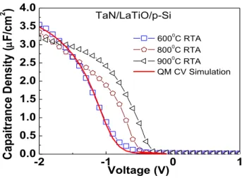
(A). High Vt challenge for gate-first MOSFET
Fig. 1 depicts the C-V characteristics of metal-gate/high- CMOS capacitors, under
3
various rapid thermal annealing (RTA) temperatures. Although very high capacitance density of 3.5 μF/cm2 was measured, or equivalent to only 0.59 nm EOT by quantum-mechanical C-V simulation, the capacitance density decreases monotonically with increasing RTA temperature from 600, 800, to 900oC. The even much more difficult challenge is the decreasing flat-band voltage (VFB) with increasing RTA temperature from 600
to 900oC, which leads to the intolerable high VT
MOSFET: ox dep F fb t C Q V V 2 (1)
Here the 2ψF, Qdep, and Cox are the surface
bending potential to inversion, depletion charge and oxide capacitance, respectively.
Fig. 1. C-V of TaN/LaTiO/p-Si MOS capacitors after different RTA temperatures. The VFB lowering for MOS
capacitor at smaller EOT is the fundamental challenge for low VT n-MOSFET.
However, such high VT is opposite to the
low power IC technology trend. Besides, the conventional self-aligned and gate-first CMOS process requires a high RTA temperature of 1000oC, where significant VFB roll-off and VT
increase were found that fail the metal-gate/ high-κ/Si n-MOSFET for modern IC application [17]. Similar VFB roll-off or metal-gate
Fermi-level pinning was also found in metal-gate/high-κ/Si p-MOSFET to cause the unacceptable high VT [20]. The VFB can be tuned
by metal work-function as:
ox ox ox f MS fb C Q C Q V (2)
Here the ΦMS, Qf, and Qox are the
metal-semiconductor work-function difference (ΦM-ΦS), fixed charge and oxide charge,
respectively. The using low or high work-function metal is the method to lower the
VT for n- or p-MOSFET, respectively. The
target metal work-functions are 4.1 and 5.2 eV for respective n- or p-MOSFETs [17], similar to doped poly-Si gate. Nevertheless, to compensate the VFB roll-off, the metal work-function
requires further adjustment to <4.1 and >5.2 eV for n- and p-MOSFETs. The only candidate in periodic table with >5.2 eV work-function is the Pt, but unfortunately the Pt will diffuse rapidly at 1000oC to cause the p-MOSFET failure [3]. This means no solution to reach low VT
metal-gate/high-κ/Si p-MOSFET with the available materials in Periodic Table! This is also the reason why it takes nearly 10 years after the first metal-gate/high-κ/Si MOSFET [13] reported in the literature.
(B). gate-last & gate-first low Vt metal-gate/
high-κ/Si MOSFET
To address this issue, Intel uses the “gate-last & replacement-gate” process [11]-[12], where the metal-gate was formed at low temperature to prevent the metal diffusion into the high-κ gate dielectric. This innovative idea indeed solves the
VFB roll-off issue and reaches the low VT
metal-gate/high-κ/Si CMOS. However, the conventional gate-first process is highly desired especially for foundry, where the cost is a major concern. Our pioneered La2O3 gate-dielectric
MOSFET has negative VFB that is ideal for
n-MOSFET [14]-[15]: -3.5 -3.0 -2.5 -2.0 -1.5 -1.0 -0.5 0.0 0.5 1.0 1.5 0 100 200 VFB=15mV C a p a c it a n c e ( p F ) Voltage (V)
Fig. 2. C-V of metal-gate/La2O3/p-Si MOS capacitors after
1000oC RTA, with negative VFB for low VT nMOS.
-2 -1 0 1 0.0 0.5 1.0 1.5 2.0 2.5 3.0 3.5 4.0 6000 C RTA 8000 C RTA 9000 C RTA QM CV Simulation TaN/LaTiO/p-Si Voltage (V) Ca pai tra nce De nsi ty ( F/ cm 2 )
4
The negative VFB for 1000oC-annealed MOS
capacitor is the ideal candidate for low VT
n-MOSFET. Our work initiates the new VFB
tuning method, using unique Qox in high-κ gate
dielectric instead of conventional ΦM
work-function tuning in eq. (2). Thus, our works were cited by IBM’s paper published in IEEE
IEDM [2] shown in Fig. 3:
Fig. 3. Our pioneered La2O3 and Al2O3 high-κ gate
dielectric MOSFET papers were cited by IBM’s paper published in IEEE IEDM.
Our La2O3 gate-dielectric MOSFET paper
also becomes the “Highly Cited Paper”, within the top 1% citation among engineering area worldwide, according to the Essential Science
IndicatorsSM of THOMSON REUTERS. In the
following, we will show the high performance low-VT p- and n-MOSFET with highly scaled
EOT, beyond the commercial available 32-nm node CMOS. The gate-first method was used because of the lower cost, simpler process, smaller layout area, and full compatibility with conventional self-aligned CMOS process.
四、研究方法及成果 A. Experimental procedure:
Standard Si substrates with ~10 ohm-cm resistivity were used in this study. For p-MOSFET, a thin SiON was first grown on 12-inch n-Si wafers. Then HfAlO of 1 nm thickness was deposited by physical vapor deposition (PVD) and followed by post- deposition annealing (PDA) at 500oC in O2 for 5
min. The adding Al2O3 into HfO2 is used to tune
the VFB to reach low-VT p-MOSFET, which is
due to the unique negative charges in the Al2O3
gate dielectric. The composition ratio of Hf and Al in HfAlO is 1:1. After that, the metal-gate was formed by depositing 50 nm MoN and 200 nm TaN by PVD and patterning. The p+ source-drain regions were formed by 35 KeV and 51015 cm-2 BF2+ implantation, followed by
1000oC RTA activation for 1 sec. Finally the Al metal was deposited for source-drain and backside contacts.
For n-MOSFET with highly scaled EOT, higher κ gate dielectric and novel low temperature source-drain junction were used. The self-aligned, gate-first TaN/LaTiO n-MOSFETs were made by 1st depositing TiO2-doped La2O3 (TiLaO) on Si by PVD,
followed by a 500oC O2 PDA. After TaN
metal-gate deposition and patterning, self-aligned 20 nm Sb n-type dopant and thin Ni were deposited and covered by a 100 nm SiO2.
Then a 650oC RTA was applied for the Ni-silicide (NiSi) induced solid-phase diffusion (SPD). After etching the non-reacted Ni similar to silicide process, an Al contact metal was added on the source-drain to form the n-MOSFETs. The fabricated MOSFETs were characterized by capacitance-voltage (C-V) and current-voltage (I-V) measurements.
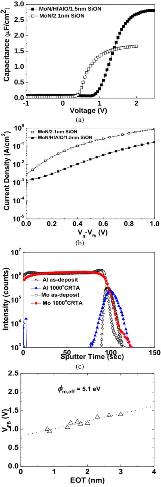
B. Device characteristics of MoN/HfAlO/
SiON/n-Si p-MOSFETs at 0.85 nm EOT:
Figures 4(a) and 4(b) show the respective
C-V and J-V characteristics of MoN/HfAlO/
1.5-nm-SiON and control MoN/2.1-nm-SiON capacitors. A ~500 mV Vfb shift, smaller EOT of
0.85 nm and low leakage current of 1.610-1 A/cm2 at 1 V of Vg-Vfb were measured for
MoN/HfAlO/1.5-nm-SiON device than the control MoN/2.1-nm-SiON sample. Such positive Vfb shift is the unique property of Al2O3
gate dielectric for low-Vt p-MOSFET. The
modulation of Vfb is attributed to the HfAlO
diffusion to SiON after 1000oC RTA, where the robust SiON blocks further diffusion into n-Si. The small EOT of 0.85 nm was obtained by considering quantum-mechanical effect. The small EOT is due to optimized inter-diffusion of HfAlO/SiON and slight diffusion of MoN gate after 1000oC RTA, as observed from SIMS measurements shown in inserted Fig. 4(c).
5 -1 0 1 2 0.0 0.5 1.0 1.5 2.0 2.5 3.0 MoN/HfAlO/1.5nm SiON MoN/2.1nm SiON Voltage (V) Ca pac itanc e ( F/cm 2 ) (a) 0.0 0.2 0.4 0.6 0.8 1.0 10-5 10-4 10-3 10-2 10-1 100 MoN/2.1nm SiON MoN/HfAlO/1.5nm SiON Vg-Vfb (V) Curr ent Density (A/cm 2 ) (b) 0 50 100 150 103 104 105 106 107 Al as-deposit Al 1000oCRTA Mo as-deposit Mo 1000o CRTA Inte ns ity (c oun ts)
Sputter Time (sec)
(c) 0 1 2 3 4 0.0 0.5 1.0 1.5 2.0 2.5 m,eff = 5.1 eV V FB (V) EOT (nm) (d)
Fig. 4. (a) C-V, (b) J-V, (c) SIMS profile, and (d) VFB-EOT
of MoN/HfAlO/1.5-nm-SiON capacitors. Control MoN/2.1-nm-SiON data were also added for comparison.
The effective work-function (m-eff) of 5.1
eV and oxide charge density of 4.5x1012 cm-2 were obtained from a Vfb-EOT plot shown in Fig.
4(d). The large m-eff is suitable for p-MOS
applications.
Figure 5 shows the gate leakage current comparison of MoN/HfAlO/SiON, poly-Si/SiO2,
MoN/2.1-nm-SiON and TaN/HfLaO gate stacks. The small 1.65 nm EOT in MoN/2.1-nm-SiON control device is also due to the slight MoN diffusion. The leakage current of 1.610-1 A/cm2 at 1 V above Vfb is ~4 orders of magnitude lower
than that of SiO2 at a 0.85 nm EOT. This low
leakage current is due to the high-HfAlO. Thus, both high m-eff and low gate dielectric leakage
current can be achieved in MoN/HfAlO/SiON MOS capacitors. 0.8 1.0 1.2 1.4 1.6 1.8 2.0 10-4 10-2 100 102 104 TaN/HfLaO [8] MoN/SiON MoN/HfAlO/SiON Benchmark J g @ 1V+ |V fb | ( A/cm 2 ) EOT (nm) Poly-Si/SiO2
Fig. 5. Gate leakage current density comparison of MoN/HfAlO/SiON, poly-Si/SiO2, MoN/2.1-nm-SiON and
TaN/HfLaO gate stacks.
In figures 6(a) and 6(b) we show the Id-Vg
characteristics and hole mobility as a function of effective electric field of the 0.85 nm EOT MoN/HfAlO/SiON p-MOSFETs, respectively. The mobility data was extracted directly from the measured Id-Vg curves at small Vd. For
comparison, the MoN/2.1-nm-SiON MOSFET with 1.65 nm EOT is also shown. A small Vt of
only -0.10 V was measured from the linear Id-Vg
plot - this is due to the high m-eff of 5.1 eV found
from the C-V measurements. Such low Vt meets
the lowest scalable value of 4kT/q for MOSFET at the end of International Technology Roadmap
for Semiconductors (ITRS) [1]. In addition, good
hole peak mobility of 80 cm2/V-s and 56 cm2/Vs at 0.8 MV/cm were obtained, at a small EOT of 0.85 nm. T slightly degraded mobility is found
6
compared with the MoN/2.1-nm-SiON control sample. The reasonable good mobility is due to the optimized SiON between high- HfAlO and Si that is critical to prevent mobility degradation.
-1.0 -0.5 0.0 0.5 10-9 10-8 10-7 10-6 10-5 10-4 10-3 MoN/HfAlO/1.5nm SiON W=100m L=10 m Vd=-0.5 V Vd=-0.1 V Dr ain Curre nt (A) Gate Voltage (V) (a) -1.00 -0.8 -0.6 -0.4 -0.2 0.0 50 100 150 200 Universal MoN/2.1nm SiON EOT=1.65 nm MoN/HfAlO/1.5 nm SiON EOT=0.85 nm Hole M o b ilit y ( cm 2 /V-sec ) Effective field (MV/cm) (b)
Fig. 6. (a) The Id-Vd and (b) hole mobility vs. effective
electric field for the MoN/HfAlO/SiON p-MOSFETs.
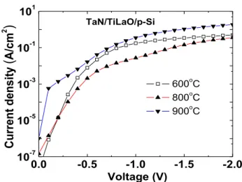
C. Device characteristics of TaN/LaTiO/p-Si
n-MOSFETs at 0.59 nm EOT:
Following the C-V characteristics of TaN/LaTiO/p-Si MOS capacitors shown in Fig. 1, Fig. 7 shows the J-V characteristics of these very small EOT capacitors. Although the leakage current was lowered after 800oC RTA, unwanted both decreasing capacitance density and Vfb
roll-off were found in Fig. 1, as the RTA temperature was increased from 600 to 900oC. We further measured Secondary Ion-Mass Spectroscopy (SIMS) to study the VFB roll-off at
high temperatures. Figure 8 shows the SIMS profile of above MOS structure after 600 and 800oC RTA. The inter-diffusion of the Ti and Si was found with increasing the RTA temperature.
0.0 -0.5 -1.0 -1.5 -2.0 10-7 10-5 10-3 10-1 101 TaN/TiLaO/p-Si 600oC 800oC 900oC Curr ent density ( A/cm 2 ) Voltage (V)
Fig. 7. J-V characteristics of TaN/TiLaO/p-Si n-MOS at various RTA temperatures.
40 60 80 100 120 140 101 102 103 104 105 106
Si
Ti
O
In tensity (cou nts) Depth (nm) RTA 600oC RTA 800o CFig. 8. SIMS profile of TiLaO after 600 and 800oC RTA treatments.
The Oxygen peak in the high- dielectric shifts towards the Si, suggesting the formation of interfacial SiOx from thermal-dynamic
considerations. This interface layer is further observed by cross-sectional Transmission Electron microscopy (TEM), which is unavoidable unless an interfacial SiO2 or SiON
is inserted between high- and Si to decrease the interface reaction and inter-diffusion. However, the inserted interfacial oxide limits further EOT down-scaling. This additional interfacial layer led to a decrease of the gate-leakage current when the RTA temperature was increased to 800oC in Fig. 7. Nevertheless, this cannot explain the unexpected leakage current decrease after 900oC RTA. We have used X-Ray Diffraction (XRD) to measure the crystallinity of the LaTiO after various RTA. As shown in Fig. 9, the amorphous LaTiO becomes crystallized at 900oC RTA. Therefore, the higher leakage
7
current after the 900oC RTA may be related to the formation of poly-crystals that provide additional leakage paths through highly-defective grain boundaries. This further emphasizes the importance of low-temperature processing to control both the interfacial reactions and the leakage current.
20 30 40 50 60 70 80 0 100 200 300 400 500 TiLaO 1000oC 900o C Intens ity (count s) 2 (degree) 600oC
Fig. 9. Grazing incidence XRD spectra of TiLaO, after various RTA treatments.
To lower the interfacial reaction and preserve the small EOT, we have used Ni-induced SPD that will drive-in the source-drain Sb dopants for TaN/LaTiO n-MOSFET. Figures 10(a) and 10(b) show the
Id-Vd and Id-Vg characteristics. Besides the well
behaved transistor characteristics, a low Vt of
0.14 V was measured at the ultra-thin 0.59 nm EOT. However, a mobility of 154 cm2/Vs was obtained in TaN/LaTiO n-MOSFET at 0.8 MV/cm with a 0.59 nm EOT, which is lower than the universal mobility of SiO2/Si
n-MOSFET. Such mobility degradation is due to the soft phonon scattering, where the electron wave-function penetrates into high-κ gate dielectric and causes additional electron scattering to lower the mobility. The degraded mobility was also widely found at metal-gate/high-n-MOSFET with small EOT less than 1 nm. The lowered mobility problem at highly scaled EOT can only be resolved by using high mobility new channel materials with smaller effective mass, such as Ge and III-V, where the defect-free integration on Si substrate was first demonstrated by our group using wafer-bonding and smart-cut to realize the Ge-on-Insulator (GeOI) [28]-[29] and III-V-on-Insulator (IIIVOI) [30]. 0.5 1.0 1.5 2.0 0 3 6 9 12 15 18 Vg = 0 V Vg = 0.5 V Vg = 1.0 V W/L = 100 / 8 m Dr ain Curre nt (mA ) Drain Voltage (V) Vg = 1.5 V Vg = 2 V (a) -1.0 -0.5 0.0 0.5 1.0 1.5 2.0 10-9 10-7 10-5 10-3 Vd = 0.1 V TaN/TiLaO/p-Si VT=0.14 V Dr ain Curr ent (A) Gate Voltage (V) (b)
Fig. 10. (a) Id-Vd and (b) Id-Vg characteristics of
self-aligned gate-first TaN/LaTiO/p-Si n-MOSFETs.
五、結論與討論
Low-Vt gate-first metal-gate/high-CMOS
was reached be using the novel oxide charge tuning that is unreachable by the conventional gate work-function tuning. Using the unique positive and negative VFB of Al2O3 and La2O3
gate dielectrics in combination with high HfO2
and TiO2, low-Vt of -0.10 and 0.14 V were
reached for n- and p-MOSFETs respectively, with small 0.85 and 0.59 nm EOT. The self-aligned and gate-first process of metal-gate/high-CMOS has merits of full compatibility with current VLSI. These technologies with small EOT can be used for several technology generations from 28-nm, 20-nm, 14-nm, even to future 10-nm node ICs.
8
六、References
[1] The International Technology Roadmap for Semiconductors, 2009 [Online]. Available: www.itrs.net
[2] D.A. Buchanan, E.P. Gusev, E. Cartier, H. Okorn-Schmidt, K. Rim, M. A. Gribelyuk, A. Mocuta, A. Ajmera, M. Copel, S. Guha, N. Bojarczuk, A. Callegari, C. D'Emic, P. Kozlowski, K. Chan, R. J. Fleming, P. C. Jamison, I. Brown, and R. Arndt, “80 nm polysilicon gated n-FETs with ultra-thin Al2O3
gate dielectric for ULSI applications,” in IEDM
Tech. Dig., 2000, pp.223-226.
[3] H.-H. Tseng, C. C. Capasso, J. K. Schaeffer, E. A. Hebert, P. J. Tobin, D. C. Gilmer, D. Triyoso, M. E. Ramón, S. Kalpat, E. Luckowski, W. J. Taylor, Y. Jeon, O. Adetutu, R. I. Hegde, R. Noble, M. Jahanbani, C. El Chemali, and B. E. White, “Improved short channel device characteristics with stress relieved pre-oxide (SRPO) and a novel tantalum carbon alloy metal gate/HfO2 stack,” in IEDM Tech. Dig., 2004, pp. 821-824.
[4] P. F. Hsu, Y. T. Hou, F. Y. Yen, V. S. Chang, P. S. Lim, C. L. Hung, L. G. Yao, J. C. Jiang, H. J. Lin, J. M. Chiou, K. M. Yin, J. J. Lee, R. L. Hwang, Y. Jin, S. M. Chang, H. J. Tao, S. C. Chen, M. S. Liang, and T. P. Ma, “Advanced dual metal gate MOSFETs with high-k dielectric for CMOS application,” in VLSI Symp.
Tech. Dig., 2006, pp. 11-12.
[5] K. Akiyama, W. Wang, W. Mizubayashi, M. Ikeda, H. Ota, T. Nabatame and A. Toriumi, “VFB roll-off in HfO2 gate stack after high
temperature annealing process - a crucial role of out-diffused oxygen from HfO2 to Si -,” in Symp.
on VLSI Tech. Dig., 2007, pp. 72-73.
[6] S. C. Song, C. S. Park, J. Price, C. Burham, R. Choi, H. C. Wen, K. Choi, H. H. Tseng, B. H. Lee, and R. Jammy, “Mechanism of Vfb roll-off with high work function metal gate and low temperature oxygen incorporation to achieve PMOS band edge work function,” in IEDM
Tech. Dig., 2007, pp. 337-340.
[7] N. Mise, T. Morooka, T. Eimori, S. Kamiyama, K. Murayama, M. Sato, T. Ono, Y. Nara, and Y. Ohji, “Single metal/dual high-k gate stack with low Vth and precise gate profile control for highly manufacturable aggressively scaled CMISFETs,” in IEDM Tech. Dig., 2007, pp. 527-530.
[8] K. L. Lee, M. M. Frank, V. Paruchuri, E. Cartier, B. Linder, N. Bojarczuk, X. Wang, J. Rubino, M. Steen, P. Kozlowski, J. Newbury, E.
Sikorski, P. Flaitz, M. Gribelyuk, P.Jamison, G. Singco, V. Narayanan, S. Zafar, S. Guha, P.
Oldiges, R. Jammy, M. Ieong,
“Poly-Si/AlN/HfSiO stack for ideal threshold voltage and mobility in sub-100 nm MOSFETs,” in Symp. on VLSI Tech. Dig., 2006, pp. 160-161.
[9] M. Kadoshima, T. Matsuki, M. Sato, T. Aminaka, E. Kurosawa, A. Ohta, H. Yoshinaga, S. Miyazaki, K. Shiraishi, K. Yamabe, K. Yamada, T. Aoyama, Y. Nara1, Y. Ohji, “Practical dual-metal-gate dual-high-k CMOS integration technology for hp 32 nm LSTP utilizing process-friendly TiAlN metal gate,” in
IEDM Tech. Dig., 2007, pp. 531-534.
[10] J. Huang, P. D. Kirsch, D. Heh, C. Y. Kang, G.
Bersuker, M. Hussain, P. Majhi, P.
Sivasubramani, D. C. Gilmer, N. Goel, M.A. Quevedo-Lopez, C. Young, C. S. Park, C. Park, P. Y. Hung, J. Price, H. R. Harris, B. H. Lee, H.-H. Tseng, R. Jammy, “Device and reliability improvement of HfSiON+LaOx/metal gate stacks for 22nm node application,” in IEDM
Tech. Dig., 2008, pp. 45-48.
[11] K. Mistry, C. Allen, C. Auth, B. Beattie, D. Bergstrom, M. Bost, M. Brazier, M. Buehler, A. Cappellani, R. Chau, C.-H. Choi, G. Ding, K. Fischer, T. Ghani, R. Grover, W. Han, D. Hanken, M. Hattendorf, J. He, J. Hicks , R. Huessner, D. Ingerly, P. Jain, R. James, L. Jong, S. Joshi, C. Kenyon, K. Kuhn, K. Lee, H. Liu, J. Maiz, B. McIntyre, P. Moon, J. Neirynck, S. Pae, C. Parker, D. Parsons, C. Prasad , L. Pipes, M. Prince, P. Ranade, T. Reynolds, J. Sandford, L. Shifren0, J. Sebastian, J. Seiple, D. Simon, S. Sivakumar, P. Smith, C. Thomas, T. Troeger, P. Vandervoorn, S. Williams, and K. Zawadzki, “A 45nm Logic Technology with High-k+Metal Gate Transistors, Strained Silicon, 9 Cu Interconnect Layers, 193nm Dry Patterning, and 100% Pb-free Packaging,” in IEDM Tech. Dig., 2007, pp. 247-250.
[12] S. Natarajan, M. Armstrong, M. Bost, R. Brain, M. Brazier, C-H Chang, V. Chikarmane, M. Childs, H. Deshpande, K. Dev, G. Ding, T. Ghani, O. Golonzka, W. Han, J. He, R. Heussner, R. James, I. Jin, C. Kenyon, S. Klopcic, S-H. Lee, M. Liu, S. Lodha, B. McFadden, A. Murthy, L. Neiberg, J. Neirynck, P. Packan, S. Pae, C. Parker, C. Pelto, L. Pipes, J. Sebastian, J. Seiple, B. Sell, S. Sivakumar, B. Song, K. Tone, T. Troeger, C. Weber, M. Yang, A. Yeoh, K. Zhang, “A 32nm logic technology featuring 2nd-generation high-k + metal-gate transistors, enhanced channel strain and 0.171
9
2
SRAM cell size in a 291Mb array,” in
IEDM Tech. Dig., 2008, pp. 941-943.
[13] A. Chin, C. C. Liao, C. H. Lu, W. J. Chen, and C. Tsai, “Device and reliability of high-k Al2O3
gate dielectric with good mobility and low Dit,”
in Symp. on VLSI Tech. Dig., 1999, p.135-136. [14] A. Chin, Y. H. Wu, S. B. Chen, C. C. Liao, and
W. J. Chen, “High quality La2O3 and Al2O3 gate
dielectrics with equivalent oxide thickness 5-10Å,” in Symp. on VLSI Tech. Dig., 2000, pp. 16-17 (Highlight Section Paper)
[15] Y. H. Wu, M. Y. Yang, Albert Chin, and W. J. Chen, “Electrical characteristics of high quality La2O3 dielectric with equivalent oxide thickness
of 5Å,” IEEE Electron Device Lett., vol. 21, pp. 341-343, July 2000.
[16] X. Yu, C. Zu, X. P. Wang, M. -F. Li, A. Chin, A. Y. Du, W. D. Wang, and D. L. Kwong, “High mobility and excellent electrical stability of MOSFETs using a novel HfTaO gate dielectric,” in VLSI Symp. Tech. Dig., 2004, pp. 110-111. [17] D. S. Yu, A. Chin, C. H. Wu, M.-F. Li, C. Zhu,
S. J. Wang, W. J. Yoo, B. F. Hung and S. P. McAlister, “Lanthanide and Ir-based dual
metal-gate/HfAlON CMOS with large
work-function difference,” in IEDM Tech. Dig., 2005, pp. 649-652.
[18] X. P. Wang, C. Shen, M.-F. Li, H. Y. Yu, Y. Sun, Y. P. Feng, A. Lim, H. W. Sik, A. Chin, Y. C. Yeo, P. Lo, and D. L. Kwong, “Dual metal gates with band-edge work functions on novel HfLaO high-κ gate dielectric,” in Symp. on
VLSI Tech. Dig., 2006, pp. 12-13.
[19] C. H. Wu, B. F. Hung, Albert Chin, S. J. Wang, W. J. Chen, X. P. Wang, M.-F. Li, C. Zhu, Y. Jin, H. J. Tao, S. C. Chen, and M. S. Liang, “High temperature stable [Ir3Si-TaN]/HfLaON
CMOS with large work-function difference,” in
IEDM Tech. Dig., 2006, pp. 617-620.
[20] C. F. Cheng, C. H. Wu, N. C. Su, S. J. Wang, S. P. McAlister and Albert Chin, “Very low Vt [Ir-Hf]/HfLaO CMOS using novel self-aligned low temperature shallow junctions,” in IEDM
Tech. Dig., 2007, pp. 333-336.
[21] C. C. Liao, Albert Chin, N. C. Su, M.-F. Li, and
S. J. Wang, “Low Vt gate-first
Al/TaN/[Ir3Si-HfSi2-x]/ HfLaON CMOS using
simple process,” in Symp. on VLSI Tech. Dig., 2008, pp. 190-191.
[22] Albert Chin, C. H. Cheng, N. C. Su, S. J. Wang, C. C. Liao, C. P. Chou, and H. L. Hwang, “Low
Vt metal-gate/high-k CMOS from understanding
the mechanism to innovative solution,” Intl.
Solid-State Devices & Materials Conf. (SSDM),,
Japan, 2008. (Invited)
[23] S. H. Lin, C. H. Cheng, W. B. Chen, F. S. Yeh, and Albert Chin, “Low Threshold Voltage
TaN/Ir/LaTiO p-MOSFETs Incorporating
Low-Temperature- Formed Shallow Junctions,”
IEEE Electron Device Lett., vol. 30, pp.
681-683, June 2009.
[24] S. H. Lin, C. H. Cheng, W. B. Chen, F. S. Yeh, and Albert Chin, “Low Threshold Voltage TaN/LaTiO n-MOSFETs with Small EOT,”
IEEE Electron Device Lett., vol. 30, pp.
999-1001, Sept. 2009.
[25] Albert Chin, M. F. Chang, S. H. Lin, W. B. Chen, P. T. Lee, F. S. Yeh, C. C. Liao, M.-F. L, N. C. Su and S. J. Wang “Flat band voltage
control on low Vt metal-gate/high-k
CMOSFETs with small EOT,” 16th Bi-Annual Conference on Insulating Films on Semiconductors (INFOS), pp. 1728–1732,
Cambridge University, UK, 2009. (Invited) [26] Albert Chin, W. B. Chen, B. S. Shie, K. C. Hsu,
P. C. Chen, C. H. Cheng, C. C. Chi, Y. H. Wu, K. S. Chaing-Liao, S. J. Wang, C. H. Kuan, and F. S. Yeh, “Metal-Gate/ High-κ CMOS scaling from Si to Ge at small EOT,” 10th Intl. Conf. on Solid-State & Integrated-Circuit Tech. (ICSICT),
2010, pp. 836-839. (Invited)
[27] D. R. Islamov, V. A. Gritsenko, A. V. Rzhanov, C. H. Cheng, and Albert Chin, “Bipolar conductivity in amorphous HfO2,” Appl. Phys.
Lett., vol. 99, p. 072109 (3 pages), Aug. 2011.
[28] C. H. Huang, M. Y. Yang, A. Chin, W. J. Chen, C. X. Zhu, B. J. Cho, M.-F. Li, and D. L. Kwong, “Very low defects and high performance Ge-On-Insulator p-MOSFETs with Al2O3 gate dielectrics,” in VLSI Symp. Tech. Dig., 2003, pp. 119-120.
[29] D. S. Yu, Albert Chin, C. C. Laio, C. F. Lee, C. F. Cheng, W. J. Chen, C. Zhu, M.-F. Li, S. P. McAlister, and D. L. Kwong, “ 3D GOI CMOSFETs with novel IrO2(Hf) dual gates and high-κ dielectric on 1P6M-0.18um-CMOS, ” in IEDM Tech. Dig., 2004, pp. 181-184.
[30] C. C. Liao, S. Kao, Albert Chin, D. S. Yu, M.-F. Li, C. Zhu, and S. P. McAlister, “Comparing High Mobility InGaAs FETs with Si and GOI Devices,” in 64th Device Research Conference
1
國科會補助專題研究計畫項下赴國外(或大陸地區)出差或研習心得報告
日期: 100 年 7 月 20 日
一、國外研究過程
日本東京大學 Prof. Toriumi 在 high-k 及 Ge MOSFET 之研究頗負盛名,與本研
究計畫主題很相關。日前雙方在加拿大蒙特屢市的 219 屆國際電化學協會研討會相
遇,筆者報告完邀請演講後,Prof. Toriumi 問了一些 high-k MOSFET 的量測問題,
我們也初步討論合作研究及筆者到東京大學訪問研究的可能性。六月中旬,Prof.
Toriumi 寄來邀請信,確定 7/2-7/11 赴該校進行訪問研究。
7 月 2 日抵達東京,進住旅館已晚。7 月 3 日赴東京大學材料系館,由研究生
帶領參觀其各實驗室、無塵室,瞭解設備與環境。7 月 4 日在東京大學材料系館,學
習瞭解 Multi-target magnetron sputtering,其利用 Laser ablation of targets,可以同時濺
鍍多元素以形成合金,是 high-k 製程研究很重要的設備。7 月 5 日赴東京大學材料系
館,學習瞭解 High pressure annealing、Rapid thermal annealing,這些設備得以改變
high-k 晶格結構。7 月 6 日赴東京大學材料系館,學習瞭解 Spectroscopic ellipsometry、
Thermal desorption meter,分析 GeO2 分解時之原子產生及擴散。7 月 7 日赴東京大
計畫編號
NSC 99- 2120 - M - 009 - 002
計畫名稱
金屬閘極/高介電係數材料互補式金氧半場效電晶體在 45 到 22 奈米世
代之應用(3/3)
出國人員
姓名
張廖貴術
服務機構
及職稱
國立清華大學工程與系統科學系
教授
出國時間
100 年 7 月 2 日至
100 年 7 月 11 日
出國地點
日本東京
2
學材料系館, 學習瞭解 Raman Spectroscopy 可以分析 graphene 之原子層數,XPS 可
分析 high-k 中鍵結與判斷 dipole。7 月 8 日赴東京大學材料系館,學習瞭解 Device
fabrication、E-beam lithography。7 月 9 日在東京大學材料系會議室,筆者報告一專
題演講,說明 Charge-pumping measurement 應用於 high-k MOSFET 的陷阱分析,Prof.
Toriumi 建議評估 displacement current 的影響,也有研究生問到如何測量 capture cross
section 等。7 月 10 日赴東京大學,由研究生帶領參觀校園及電機系等單位重要設施。
7 月 11 日赴東京大學,自行參觀校園及附近設施,午後搭機回台。
二、研究成果
此次訪問研究之心得,主要在 high-k 及 Ge MOSFET,也大致瞭解 graphene 之研究,
分別敘述如下,
1. High-k dielectrics
(a) 由多元素合金改變結構以增加 high-k 介電係數
例如 Y2O3 into HfO2、Si-doped HfO2、LaYOx、及 LaTaOx 等。
(b) 以 Rapid Thermal Treatment 控制 high-k 結構及介電係數
(c) 介電層雙偶極(dipole)之形成
MOS 元件 Vfb 偏移以 dipole formation 之理論解釋受到重視,也藉由鍵結能量
改變(shift of binding energies by XPS)驗證,有許多研究及論文都引用此機制。
Dipole formation 可能是介電層之間氧密度不同產生應力,驅使 dipole 產生。
2. Ge MOSFET
(a) GeO2 在 GeO2/Ge 介面分解
3
電特性不佳。分解成 GeO 後,GeO 之擴散將限制其繼續分解。
(b) 高壓氧化 GeO2/Ge 界面
在 GeO2/Ge 施以高壓氧化,在熱動能上可以抑制 GeO2 之分解而改善界面
與 GeO2 電特性,製作 Ge MOSFET,觀察到 mobility 相當高。
(c ) 以稀土元素及高壓氧化改善 high-k/Ge 界面
例如以 LaLuO on Ge 可以鈍化(passivate)界面,而改善 MOS 元件電特性。
(d) Fermi level pinning at metal/Ge interface
金屬與鍺之接觸,能帶差與金屬功函數無關,僅與鍺 Ef 能階有關,此機制
仍待研究。經由一層很薄的氧化層在 metal/Ge 中間,能將 Schottky-ohmic 接
觸做轉換,因此 n+ junction 可利用此方法,減少 metal/Ge 接觸電阻,製作特
性佳的 n-channel Ge MOSFET。
3. Graphene FET
Graphene 是近來很熱門的奈米材料,由於有極高的 carrier mobility,與一般
CMOS 製程匹配,很受重視。研究初步,要先解決如何由石墨層撥離出 graphene。
然後須測量 graphene/metal interface 之接觸電阻,是 Graphene 應用於奈米電子元
件之關鍵。
綜合以上研究心得,該研究群在 Ge 基材上成長閘介電層及分析研究,藉由先形成
GeO or GeN 在 Ge 基材,然後沉積 HfO2 介電層,及適當高氣壓或快速退火處理,可
以改善介電層之熱穩定與漏電流等。再者,半導體元件之材料及電特性測量分析,
其所須投入的資源不必多,但是成果卻可能非常重要,從該研究群的幾篇精彩論文
即可看出,其研究規劃很好,所以探討的機制很深入,並不需複雜的分析或貴重設
備。有些 high-k 製程研究很值得學習,例如 LaGeO 的製程探討,就是將兩種最新穎
4
材料整合研究,爾後類似元素應可再研究開發。
三、建議
赴國外研究享負盛名之實驗室訪問研究,對研究人員新知之取得,最新研發方
向的瞭解確有極大的幫助,此方面之補助經費並不多,希望國科會持續或更加
強。
四、其他
本次訪問研究,雙方亦討論國科會與日本科學技術振興機構(NSC/JST)雙邊
共同合作計畫之可能性,惟每件計畫每年平均最高補助經費為五佰萬日圓,日
方學者對國際合作研究比較保守,此預算對他們較低,也難引發興趣。
Travel Report
IEEE Electron Devices Society AdCom and IEEE International Electron Devices Meeting
由於服務於 IEEE Electron Device Society 擔任 Technical Committee 及 IEEE International Electron Devices Meeting 之 Executive Committee,我於 12 月 4 日下 午搭乘長榮航空公司之飛機,抵達 San Francisco 機場時,已下午三點了,再搭 乘 BART 捷運至旅館,放下行李時,已經近 5 點了。而 IEEE Electron Devices AdCom 於星期六早上開始,因此略加整理後即到大會舉辦之 Hilton 旅館。 第二天一大早再去開 Electron Devices Society AdCom 會議,中午時我們並討論 了,將在 IEEE Trans. Electron Devices 期刊,出版 Special Issue 的工作可行性。 此會議一直到晚上 9 點才結束。然另外 International Electron Devices Meeting 之 會前會即在晚上 8 點舉行,所以我們於 7:30 即離開 AdCom,前往接下來之另 一會議。
此 International Electron Devices Meeting 為 IEEE Electron Devices Society 之 最主要的會議,這也是為何 AdCom 選在前兩天舉行之故,因主要 IEEE Electron Devices Society 之會員,均會來參加此會議。此「會前會」之主要參與人員為 Executive Committee 及各 Section Chair & Co-Chair。而「會前會」不但有清點各 Section Chair 是否由全球各國到達會場外,並報告了 Section Chair & Co-Chair 之 職責,因亞洲各國(新加坡及印度除外)均非英語系國家,因此我必須負責為各個 演講者找英文翻譯,如演講者來自日本,我們必須找精通日語、英語者,且為同
領域並參加本次 International Electron Devices Meeting 者,因此我和我的日本藉 Co-Chair 花了很多時間安排,方找到適合人選擔任 English Language Translator。 本次 International Electron Devices Meeting 於 12 月 6 日星期一早上正式舉 行,而第一位 Plenary Invited Speaker 為 Kinam Kim President & CEO of Samsung Advanced Institute of Technology。此研究院為三星電子最尖端的研發單位,因此 President Kim 報告了三星電子未來發展的願景及達成此目標的先進元件研發。其 包 含 的 範 圍 從 Display Technology 、 three dimensions Flash memory 、 new non-volatile memory、 new metal-gate/high-k/Ge-ⅢⅤCMOS Logic 、near future energy/power device etc。如果能達到這些目標,人類世界將進入另外一新科技時 代!而三星電子規畫成功的時間卻只在未來 5~10 年短期內。如三星電子能在這些 領域成功,將對台灣 DRAM、Display、LED、Flash Memory 等產業的公司造成 致命性的打擊。所幸我們在 Flash Memory、new ultra-low energy non-volatile memory、flexible plastic electronics and metal- gate/high-k/Ge MOSFET 各方面均有 重大的突破,發表以下論文於 International Electron Devices Meeting 而我們在這 些領域均超越三星電子及韓國大學的教授。而我們發表論文後,均為 Intel、 SanDisk 等 Logic 及 Memory 大公司所詢問,並向我們要求發表的投影片電子檔。 我們的 metal- gate/high-k/Ge MOSFET 為目前的世界記錄,其 performance 超越 Stanford University 的 Ge MOSFET,並較 Intel 的 metal- gate/high-k/Si MOSFET 具有相同先進的 equivalent-oxide-thickness(EOT),然而我們的 MOSFET 卻有更高
的 electron mobility。我們的 ultra-low energy resistive RAM(RRAM)為世界上首次 之新的 non-volatile memory 具有如傳統 Flash Memory 相近的 Switching Energy, 然卻具有 10000 倍更高的速度,更佳的 Program/Erase endurance,更便宜的製造 成品等優勢。
本次 International Electron Device Meeting 於 12 月 9 日星期三下午結束,在 經 Executive Committee 會後會討論後,圓滿結束。我於星期四凌晨搭長榮航空 飛機返台,到達台灣時已是星期五早上了。本次行程參加此二會議,經一些困難 克服後,圓滿結束。
國科會補助計畫衍生研發成果推廣資料表
日期:2011/10/26國科會補助計畫
計畫名稱: 金屬閘極/高介電係數材料互補式金氧半場效電晶體在45到22奈米世代之應用 (3/3) 計畫主持人: 荊鳳德 計畫編號: 99-2120-M-009-002- 學門領域: 奈米儀器設備與發展研發成果名稱
(中文) 金屬閘極/高介電係數材料互補式金氧半場效電晶體在45到22奈米世代之應用 (3/3)(英文) METAL-GATE/HIGH-κ/GE MOSFET WITH LASER ANNEALING AND
FABRICATION METHOD THEREOF
成果歸屬機構
國立交通大學發明人
(創作人)
荊鳳德技術說明
(中文) 金氧半場效電晶體一般使用鍺通道能提供較高的Veff和高的電子遷移率,來改善 汲極電流,然而不好的高介電常數和鍺的接面及在使用離子佈值的源極及汲極上 的低參雜活性離子是鍺的金氧半場效電晶體面臨的最大問題,因此為了改善這些 問題,我們設計了金屬閘極/高介電係數層/鍺 金氧半場效電晶體使用雷射退火和 製造方法去達到能同時改善接面的品質和高場效電子遷移率,所以能應用於鍺金 氧半場效電晶體,解決目前市場上迫切的需求(英文) To improve the Id, Ge channel is used for MOSFET to provide higher veff and high-field
mobility. The poor high-κ/Ge interface and low doping activation at ion-implanted source-drain are the main issue for Ge MOSFET.
Thus, for the demand, designing a metal-gate/high-κ/Ge MOSFET with laser annealing and a fabrication method thereof to achieve both better interface quality and high-field mobility in metal-gate/ high-κ/Ge MOSFETs has become an urgent issue for the application in the market.
產業別
其他專業、科學及技術服務業技術/產品應用範圍
metal-gate/ high-κ/Ge MOSFET技術移轉可行性及
預期效益
need to talk with TEL
99 年度專題研究計畫研究成果彙整表
主 持 荊 鳳計畫編號: 99-2120-M-009-002-名稱:金屬閘極/高介電係數材料互補式金氧半場效電晶體在 45 到 22 奈米世代之應用(3/3) 量化 項目 實際 已達 成數 (被 接受 或已 發 表) 預期 總達 成數 (含 實際 已達 成 數) 本 計 畫 實 際 貢 獻 百 分 比 單 位 備註(質 化 說 明 : 如 數 個 計 畫 共 同 成 果 、 成 果 列 為 該 期 刊 之 封 面 故 事 ...等) 期 刊 論 文 0 0 10 0% 研 究 報 告 / 技 術 報 告 0 0 10 0% 研 討 會 論 文 0 0 10 0% 篇 文 作 專 書 2 2 10 0% 申 請 中 件 數 0 0 10 0% 利 已 獲 得 件 數 2 2 10 0% 件 術 件 2000 2000 10 件數 0% 轉 權 利 金 42 42 10 0% 千 元 碩 士 生 31 31 10 0% 博 士 生 2 2 10 0% 博 士 後 研 究 員 2 2 10 0% 與 畫 力 本 國 ) 專 任 助 理 0 0 0% 人 次
IEEE Fellow ’for contributions to high-K dielectrics and metal gate electrodes complementary metal-oxide semiconductor’
國際會議 Tutorial 及 Invited Talks:
Si Nanoelectronics Workshop (SNW), 2011. (Panelist) SanDisk, USA 2011. (invited talk)
Materials Research Society (MRS), San Francisco, USA, April, 4-8, 2010. (Tutorial & Se Chair)
3D Transistor Workshop, Japan 2010 (Director Yushiro Nishi, Stanford). (invited t 16th Bi-Annual Conference on Insulating Films on Semiconductors (INFOS), Camb University, UK, June 29~July 1, 2009. (invited talk)
7th Intl. Symposium on High Dielectric Constant Materials and Gate Stacks, 216th El Chemical Society (ECS), Vienna, Austria, Oct. 4-9, 2009. (invited talk)
Intl. Solid-State Devices & Materials Conf. (SSDM), (IEEE), Tsukuba, Japan, Sept. 2 2008. (invited talk)
Intl. Symp. on Advanced Gate Stack Technology (ISAGST), (IEEE), Austin, Texas Sept.29-Oct. 1, 2008. (invited talk)
國際合作:Tokyo Electron Ltd. (TEL), Natl. Inst. of Advanced Industrial Science & Techn 受國際主要媒體「紐約時報」’New York Times’訪問 (Dec. 15, 2008)-首次於台灣電子元件 界之研發: http://bits.blogs.nytimes.com/2008/12/15/for-chip-makers-hybrids-may-be-a-way-for 期 刊 論 文 46 46 10 0% 文 作 研 究 0 0 10 0% 篇
報 告 / 技 術 報 告 研 討 會 論 文 33 33 10 0% 專 書 3 3 10 0% 章 / 本 申 請 中 件 數 1 1 10 0% 利 已 獲 得 件 數 2 2 10 0% 件 件 數 2000 2000 10 0% 件 術 轉 權 利 金 0 0 10 0% 千 元 碩 士 生 0 0 10 0% 博 士 生 0 0 10 0% 博 士 後 研 究 員 0 0 10 0% 與 畫 力 外 國 ) 專 任 助 理 0 0 10 0% 人 次
成 法 化 之 如 學 活 獲 獎 重 際 、 成 際 力 他 產 術 之 效 項 請 字 填 果項目 量化 名稱或內容性質簡述 驗工具 質 性 量性) 0 程 / 模 0 腦及網 系統或 具 0 材 0 辦之活 競賽 0 討 會 / 作坊 0 子報、 站 0 畫成果 廣之參 閱聽) 數
國科會補助專題研究計畫成果報告自評表
請就研究內容與原計畫相符程度、達成預期目標情況、研究成果之學術或應用價
值(簡要敘述成果所代表之意義、價值、影響或進一步發展之可能性)
、是否適
合在學術期刊發表或申請專利、主要發現或其他有關價值等,作一綜合評估。
1. 請就研究內容與原計畫相符程度、達成預期目標情況作一綜合評估
■達成目標
□未達成目標(請說明,以 100 字為限)
□實驗失敗
□因故實驗中斷
□其他原因
說明:
2. 研究成果在學術期刊發表或申請專利等情形:
論文:■已發表 □未發表之文稿 □撰寫中 □無
專利:■已獲得 □申請中 □無
技轉:■已技轉 □洽談中 □無
其他:(以 100 字為限)
In this 3 years' project, we have published 6 papers in premier IEEE International Electron Devices Meeting (IEDM), 2 papers in Symp. on VLSI, 1 in Advanced Materials, got a new IP on laser annealing process for advanced CMOS, joint development projects with Tokyo Electron Ltd. (TEL). The Laser Annealing has been listed in Intel's roadmap for Highly Scaled CMOS at sub-15 nm nodes.
3. 請依學術成就、技術創新、社會影響等方面,評估研究成果之學術或應用價
值(簡要敘述成果所代表之意義、價值、影響或進一步發展之可能性)(以
500 字為限)
我們全世界首創的高介電係數閘極氧化層(high-κ) La2O3 和 Al2O3,IBM 聯盟(IBM, Samsung, Toshiba, Global foundries etc) 已成功於 2010 年應用至 32 奈米節點的 metal-gate/high-κ CMOSFET,此乃由於 high-κ La2O3 和 Al2O3 獨特的正、負電荷,使 「 平 帶 電 壓 」 的 調 整 達 到 低 的 「 起 始 電 壓 」。 這 個 閘 極 優 先 製 程 比 Intel 的 replacement-gate & gate-last 製程簡單且經濟,此外 high-κ La2O3 也具有相對於矽的 較大導帶差和比 HfO2 大的κ值。IBM 聯盟的 32 奈米技術節點的 metal-gate/high-κ CMOSFET 已 在 2010 年 成 功 量 產 , 其 nMOS 的 「 等 效 氧 化 層 厚 度 」 (equivalent-oxide-thickness, EOT) 接 近 於 Intel 但 於 pMOS 稍 大 。 我 們 的 metal-gate/high-κ CMOSFETS 有非常小的「等效氧化層厚度」(0.6~0.7 奈米),較低的 起始電壓(<0.2V)。我們另一個優勢是在較佳的微縮下,漏電流比 Intel 的元件小 4 個數 量級。
因為我們的研究貢獻,計畫主持人荊鳳德教授穫得 IEEE Fellow ’for contributions to high-K dielectrics and metal gate electrodes for complementary metal-oxide semiconductor’,而 TSMC R&D Vice President 亦寫 email 恭喜我們穫得 IEEE Fellow。
我們的研究團隊亦受邀請到國際會議 Tutorial 及 Invited Talks: Si Nanoelectronics Workshop (SNW), 2011. (Panelist)
SanDisk, USA 2011. (invited talk)
Materials Research Society (MRS), San Francisco, USA, April, 4-8, 2010. (Tutorial & Section Chair)
3D Transistor Workshop, Japan 2010 (Director Yushiro Nishi, Stanford). (invited talk)
16th Bi-Annual Conference on Insulating Films on Semiconductors (INFOS), Cambridge University, UK, June 29~July 1, 2009. (invited talk)
7th Intl. Symposium on High Dielectric Constant Materials and Gate Stacks, 216th Electro Chemical Society (ECS), Vienna, Austria, Oct. 4-9, 2009. (invited talk) Intl. Solid-State Devices & Materials Conf. (SSDM), (IEEE), Tsukuba, Japan, Sept. 24-26, 2008. (invited talk)
Intl. Symp. on Advanced Gate Stack Technology (ISAGST), (IEEE), Austin, Texas USA Sept.29-Oct. 1, 2008. (invited talk)
國際合作:Tokyo Electron Ltd. (TEL), Natl. Inst. of Advanced Industrial Science & Technology
且受國際主要媒體「紐約時報」’New York Times’訪問 (Dec. 15, 2008)-首次於台灣 電子元件學術界之研發:
http://bits.blogs.nytimes.com/2008/12/15/for-chip-makers-hybrids-may-be-a-way -forward/