國 立 交 通 大 學
電子工程學系 電子研究所碩士班
碩 士 論 文
高壓 BCD 製程之靜電放電防護元件
設計與實現
Study of Electrostatic Discharge Protection
Devices in High-Voltage
BCD Technology
研 究 生: 許哲綸 (Che-Lun Hsu)
指導教授: 柯明道教授 (Prof. Ming-Dou Ker)
高壓 BCD 製程之靜電放電防護元件
設計與實現
Study of Electrostatic Discharge Protection
Devices in High-Voltage
BCD Technology
研 究 生:許哲綸 Student:
Che-Lun
Hsu
指導教授:柯明道教授
Advisor:
Prof.
Ming-Dou
Ker
國立交通大學
電子工程學系
電子研究所
碩士論文
A Thesis
Submitted to Department of Electronics Engineering and Institute of Electronics
College of Electrical and Computer Engineering
National Chiao-Tung University
in Partial Fulfillment of the Requirements
for the Degree of
Master
in
Electronics Engineering
August 2009
Hsin-Chu, Taiwan
中華民國九十八年八月
高壓 BCD 製程之靜電放電防護元件
設計與實現
學生:許哲綸
指導教授:柯明道教授
國立交通大學 電子工程學系電子研究所碩士班
ABSTRACT (CHINESE)
在 smart power technology 中,高壓 (high-voltage, HV) 電晶體已經廣泛運用 在顯示器積體電路 (integrated circuits, ICs) 、電源供應 (power supplies) 、電源 管理 (power management) ,和汽車電子 (automotive electronics) 應用上。為了 克服在高壓電晶體中的高工作電壓,製程上的複雜度與確保高壓元件可靠度的困 難度也隨之增加。因此,在如此惡劣工作環境下所引發的栓鎖 (latch-up) 現象對 於在靜電放電 (electrostatic discharge, ESD) 可靠度的考量上更具有挑戰性。
有效率的靜電放電防護設計對於要求可靠度的高壓電晶體而言是極重要 的。為了確保靜電放電防護元件的效率和可靠性,其靜電放電防護元件的電壓-電流 (I-V) 特性曲線圖必須落在靜電放電防護設計窗口 (ESD protection design
window) 的範圍內。也就是說靜電放電防護元件的觸發電壓 (trigger voltage, Vt1)
必須比內部電路的崩潰電壓 (VBD, internal) 還要低,且靜電放電保護元件的持有電
壓 (Vhold) 必須大於工作電壓 (VDD) 。
在高壓製程中,雙載子接面電晶體 (bipolar junction transistors, BJTs) 、高壓 金氧半場效電晶體 (HV MOSFET) 和矽控整流器 (silicon controlled rectifier, SCR) 已經普遍被當作靜電放電防護元件。在這些元件中以矽控整流器最為吸引
injection) 和寄生的正回授機制 (regenerative feedback mechanism) 所造成矽控整 流器的低持有電壓特性將會導致被當做電源間靜電放電箝制電路 (power-rail ESD clamp circuit) 使用的矽控整流器更容易發生栓鎖現象。因此,增加靜電放 電防護元件的持有電壓和降低栓鎖現象的發生是高壓靜電放電防護設計中重要 的課題。 在高壓製程中,許多針對增加靜電放電防護元件的栓鎖免疫能力已經被發 展。其中一種方法是增加靜電放電防護元件的持有電壓使大於工作電壓,另一個 方法是增加靜電放電防護元件的觸發電流 (Itrig) 或持有電流 (Ihold) 使大於最小 的栓鎖觸發電流 (ILU) 。因為栓鎖現象是一種毫秒的可靠度測試,所以在判斷栓 鎖免疫能力上使用 DC 量測的持有電壓、觸發電流和持有電流比使用傳輸線系統 (transmission-line-pulsing, TLP) 量測的值當作依據更具有說服力。 在本篇論文中,具有高栓鎖免疫能力的靜電放電防護元件已被設計與發展並 成功的在 0.5-µm 16-V bipolar CMOS DMOS (BCD) 製程中獲得驗證。在整篇論 文中採用矽控整流器當做靜電放電防護元件因為其具有優秀的靜電放電防護表 現。從 DC 的量測結果發現,藉由 N+-Buried Layer (NBL) 的加入可以增加矽控 整流器的持有電流。另外,具有高暫態栓鎖免疫能力的靜電放電防護架構可以利 用堆疊元件的方式去實現。
Study of Electrostatic Discharge Protection
Devices in High-Voltage
BCD Technology
Student:
Che-Lun
Hsu
Advisor:
Prof.
Ming-Dou
Ker
Department of Electronics Engineering &Institute of Electronics
College of Electrical and Computer Engineering
National Chiao-Tung University
ABSTRACT (ENGLISH)
High-voltage (HV) transistors in smart power technologies have been extensively used for display driver integrated circuits (ICs), power supplies, power management and automotive electronics. However, the process complexity and the difficulty to guarantee the reliability of HV devices are greatly increased for the sake of sustaining such high operating voltage in HV ICs. As a result, the electrostatic discharge (ESD) reliability becomes challenging due to the severe latch-up threat in such a harsh environment.
The ESD protection design with high efficiency is vital to the HV ICs for the requirement of reliability. To ensure the effectiveness and reliability of an ESD protection design, it has been generally approved that the I-V characteristics of ESD protection devices should locate within the ESD protection design window which defines the trigger voltage (Vt1) of ESD protection devices to be lower than the both
snapback holding voltage (Vhold) larger than the power supply voltage (VDD).
In HV technology, bipolar junction transistors, HV MOSFET and silicon controlled rectifier (SCR) have been used as on-chip ESD protection devices. Among the ESD protection devices, the SCR device is attractive and applicable for ESD protection because it exhibits extremely high failure current and low dynamic on-resistance with occupying the smallest layout area. Unfortunately, the impact of extremely low holding voltage resulted from double-carrier injection and inherent regenerative feedback mechanism causes SCR to be susceptible to quasi-static latch-up or transient-induced latch-up (TLU) danger under normal circuit operating condition, especially while SCR is used in the power-rail ESD clamp circuit. Consequently, ESD design effort is usually focused on boosting the holding voltage of ESD protection devices and minimizing the latch-up risk in HV ICs.
Several ESD protection structures aimed at increasing the latch-up immunity have been investigated and reported in HV ICs. One way is to increase the holding voltage of ESD protection devices to be larger than the power supply voltage, and the other way is to increase the trigger or holding current of ESD protection devices above certain minimum latch-up triggered current to prevent latch-up during normal circuit operating condition. In addition, the ESD protection devices immunity against latch-up referred to the transmission-line-pulsing (TLP)-measured holding voltage, holding current and trigger current is insufficient because the latch-up event is a reliability test with the time duration longer than millisecond. Therefore, the holding voltage, holding current and trigger current measured from a dc curve tracer is more convincing than that measured by the TLP system while judging the validity of latch-up susceptibility.
In this thesis, the ESD protection devices with high latch-up immunity have been designed and developed, and successfully verified in a 0.5-µm 16-V bipolar CMOS
DMOS (BCD) processes. The SCR devices are adopted as ESD protection devices in this work because of their superior ESD performance. From the dc experimental results, the high holding currents of the single SCR devices are accomplished by the implantation of N+-buried layer (NBL). Besides, the high immunity against transient-induced latch-up can be realized by the stacked configuration of SCR devices.
ACKNOWLEDGEMENTS
致謝
在這兩年充實的碩士生涯當中,首先我要感謝我的指導教授 柯明道老師。 老師在接任義守大學副校長職位之後瘋狂的忙碌,瘋狂的奔波南北兩地。老師的 體力很好,即使開會開得很晚了老師還是神采奕奕、精神抖擻的指導我們。我在 一旁看都覺得老師很辛苦,希望老師身體能夠永遠保持健康,GO! GO! GO!
而在我的研究過程中,我要特別感謝「世界先進股份有限公司」給予我們研 究群許多下線機會,讓我們有機會對我們的電路和元件做一個很好的驗證。 當然啦! 在我頭上的另一個老大就是陳穩義學長。學長人很 nice,很讚!每 次我有研究上的問題,問學長就萬事 OK,很穩當很妥當的啦!就像學長的名字 一樣穩。在此,受小弟深深的一鞠躬,感恩囉!阿里阿多!!! 接下來就是和我同甘共苦的大家啦!人數眾大,讓小弟娓娓道來。這一路走 來從不相識到淺淺的認識最後進入無話不談的感情變化真是令人擋也擋不住,一 發不可收拾,就這樣或許是研究革命的情感,大家一起熬夜 Layout,一起在背後 說別人壞話(叔叔有練過,小朋友不要學),一起度過許多單身的日子(可以不要 嗎 XD),一起打籃球(我要打 10 輪!),一起打嘴炮(讓專業的來),一起打 XBOX(感 謝陸小小的大力贊助,雖然你連惡靈古堡都沒有破關,加油好嗎!!!),這段兩年 的時光還真是有給它豐富到,所有與夥伴的情感都在一瞬間堆砌,推得很滿很 滿,哪天我離開了這個小團體,懷念加上不捨我想是最基本配備吧!!! 再來換響亮亮的夥伴登場,我要大感謝有著紙紮意志力的陸小小,漂亮寶貝 佳琪,團購天后翁姊,動力水肥車的喪盡天良,喜歡高白瘦正的溫教練,躺在椅 子上也可以睡很久的阿戴爾,喜歡偷偷來的 low 雲,愛訂河粉的小凡,愛補刀的 余翔詮,勇闖博班地獄的彥偉,美食專家的 kitty 貓,實驗室管理員的天天開心, 喜歡拍照的世昕,以及長老五人眾歐ㄟ,宗恩,歐陽,Ker Ker 和宅哥。大感謝 大感恩囉! 最後要感謝的人太多了,那就只好感謝上蒼吧!若有遺漏,在此一併謝過。 本論文撰寫時已力求嚴謹,然謬誤之處在所難免,尚祈各位讀者不吝惜賜予寶貴 意見,使本論文能更加完善。 許 哲 綸 謹誌於竹塹交大 民國九十八年八月
CONTENTS
ABSTRACT (CHINESE) ...i
ABSTRACT (ENGLISH) ... iii
ACKNOWLEDGEMENTS ...vi
CONTENTS...vii
TABLE CAPTIONS ...ix
FIGURE CAPTIONS...x
Cheapter 1 Introduction...1
1.1 Motivation...1
1.2 Scheme of ESD Protection Design in High-Voltage (HV) ICs...1
1.3 ESD Protection Design Window of HV ESD Protection Devices...2
1.4 Investigation on the Impact of Kirk Effect to HV ESD Protection Devices....4
1.5 Investigation on the Impact of Kirk Effect to Holding Voltage [8] ... 11
1.6 Brief Summary...15
Cheapter 2 Prior Designs of Latch-up Immunity Increase...16
2.1 Holding Voltage Increase by Segmented Emitter Topology [9] ...16
2.2 Holding Voltage Increase by Stacked Configuration Topology [10] ...20
2.3 Holding Voltage Increase by Gate-Controllable Topology [11] ...25
2.4 Holding Voltage Increase by Implantation of N-Buried Layer [12] ...30
2.5 Trigger Current Increase by PMOS-Triggered HVSCR [13] ...35
2.6 Brief Summary...38
Cheapter 3 Parameters Investigation on Holding Voltage of SCR...39
3.1 Latch-up Immunity Considerations under Normal Circuit Operating Condition...39
3.2 Investigation on Holding Voltage increase of HVSCR...41
3.3 Investigation on the Engineering of Trigger and Holding Voltage Increase of HV SCR ...44
4.1 Impact of N-Buried Layer (NBL) Implantation on Single SCR Devices ...47
4.1.1 SCR with Different Lengths of Anode to Cathode ...47
4.1.2 SCR with Crossed Anode and Cathode ...57
4.1.3 SCR with Extended Anode ...62
4.1.4 SCR with Change Side of P+ and N+ Diffusions in the Cathode (Modified SCR) ...65
4.2 Brief Summary...74
Chapter 5 Proposed Designs of Stacked SCR Devices with Efficient Trigger Circuits ...76
5.1 Diode-Breakdown-Trigger SCR (DBTSCR) with Current Mirror Trigger Circuits ...76
5.2 HV P-Type SCR (HVPSVR) and HV N-Type SCR (HVNSCR) with RC-Based Trigger Circuits...93
5.3 Brief Summary... 115
Chapter 6 Conclusions and Future Works ... 116
6.1 Conclusions... 116
6.2 Future Work ... 117
REFERENCES ... 118
TABLE CAPTIONS
Table 4.1 The measurement results of SCR with different positions of NBL
implantation while DAC are 20µm...55 Table 4.2 The measurement results among the striped type SCR and crossed type SCR and crossed type SCR with NBL ...59 Table 4.3 The measurement results of the anode-extended SCR devices with and
without NBL ...63 Table 4.4 The measurement results of typical and modified SCR devices...69 Table 5.1 The measurement results of the DBTSCR ...91 Table 5.2 The measurement results of HVPSCR and HVNSCR and stacked HVPSCR
FIGURE CAPTIONS
Figure 1.1 The scheme of whole-chip ESD protection design in HV ICs ...2 Figure 1.2 The ESD protection design window of HV ESD protection devices ...4 Figure 1.3 The onset schemes of Kirk effect in BJT devices of (a) p-n-p devices and (b)
n-p-n devices ...6 Figure 1.4 The devices cross-sectional views with parasitic bipolar transistors and the
variations of electric field in (a) DDDPMOS devices and (b) LDNMOS devices under the onset of Kirk effect ...7 Figure 1.5 The cross-sectional views of nDEMOS...8 Figure 1.6 The simulated impact ionization region inside an nDEMOS in (a)
breakdown state and (b) snapback state due to the Kirk effect ...9 Figure 1.7 The cross-sectional views of RESULF LDMOS...10 Figure 1.8 The device simulation data on the junction temperature profile within the
LDNMOS during the snapback breakdown condition ...10 Figure 1.9 The I-V curves for different current regimes of ggLDNMOS: breakdown,
BJT triggering, snapback and high current region after holding voltage ...13 Figure 1.10 Minority carriers (avalanche hole) injection into the n-epi depending on
the depth perpendicular below the FOX (see inset) ...13 Figure 1.11 Impact ionization rates for different current regimes of ggLDMOS ...14 Figure 1.12 Dependence of holding voltage from the ration of the number of electrons
that reach the drain to number of avalanche amplified electrons...14
Figure 2.1 The cross-sectional view of triple-well SCR structure...16 Figure 2.2 The top views of SCR with (a) traditional stripe topology and (b) novel
segmented topology...17 Figure 2.3 The TLP-measured I-V characteristics for two SCR devices with the stripe
and segmented topologies...18 Figure 2.4 The TLP-measured I-V characteristics of SCR devices with different
segment ratios and D5= D6= 8µm...18 Figure 2.5 The TLP-measured I-V characteristics of SCR devices with 1:1 segment
ratio having four D5/ D6 lengths...19 Figure 2.6 The cross-sectional view of high-voltage field-oxide (FOD) device ...20 Figure 2.7 The measurement setup of single high-voltage FOD device and
stacked-field-oxide structure under TLP stress ...21 Figure 2.8 The TLP-measured I-V characteristics of single FOD and stacked FOD
and W2 is the channel width of FOD2 ...21 Figure 2.9 The TLP-measured I-V characteristics of the stacked FOD devices with
different substrate-triggered currents...22 Figure 2.10 Measurement setup for TLU test ...23 Figure 2.11 The measured waveforms on the stacked-field-oxide structure under TLU
test with (a) positive charging voltage and (b) negative charging voltage24 Figure 2.12 The (a) equivalent circuit and (b) cross-sectional view of the GC-HVSCR
device...27 Figure 2.13 The simulated 2-D current flow lines of the GC-HVSCR under (a) normal circuit operating and (b) ESD stress conditions ...28 Figure 2.14 The TLP-measured I-V characteristics of the GC-HVSCR under (a)
normal circuit operating and (b) ESD stress conditions...29 Figure 2.15 Measurement of the temperature dependence of the holding voltage of
GC-HVSCR under normal circuit operating condition...30 Figure 2.16 The cross-sectional view of the NPN bipolar transistor ...31 Figure 2.17 The TLP-measured I-V characteristics of the NPN bipolar transistor under different d values ...31 Figure 2.18 The migrations of impact ionization region in the NPN bipolar transistor
at different current levels...33 Figure 2.19 The (a) TLP-measured I-V characteristics for variations of the parameter t
and (b) linear dependence on the parameter t and the breakdown and trigger voltages ...34 Figure 2.20 The equivalent circuit of PMOS-triggered HVSCR...36 Figure 2.21 The TLP-measured I-V characteristics of PMOS-triggered SCR ...37
Figure 3.1 Solutions to enhance the latch-up immunity by (a) trigger current increase and (b) holding current increase and (c) holding voltage increase under normal circuit operating condition...40 Figure 3.2 The sketch of voltage drops in the SCR device...41 Figure 3.3 The sketches of (a) increasing RC, PNP and (b) increasing RC, NPN and
(C) decreasing RB, NPN and (d) decreasing RB, PNP to boost the holding voltage of SCR devices ...43 Figure 3.4 The engineering of trigger and holding voltages of the SCR device...44 Figure 3.5 The sketches of decreasing the base resistance of NPN transistor in SCR
device by (a) the gate-controlled NMOS and (b) the base-controlled NPN transistor ...45
Figure 4.1 The cross-sectional views of single SCR devices (a) without NBL and (b) with NBL under cathode and (c) with NBL under anode and cathode and (d) with NBL under anode ...48 Figure 4.2 The (a) TLP-measured I-V characteristics of SCR with different DAC and (b)
the comparisons of holding and trigger voltages under different DAC under
the absence of NBL implantation ...49 Figure 4.3 The (a) TLP-measured I-V characteristics of the single SCR devices with
different NBL positions while DAC are 5µm and (b) SCR devices with
different NBL positions while DAC are 20µm ...51
Figure 4.4 Comparisons of the holding and trigger voltages and (b) the HBM level and MM level among the single SCR devices under different positions of NBL implantation while DAC are 20µm ...52
Figure 4.5 Migrations of avalanche region in SCR (a) without NBL and (b) with NBL under cathode and (c) with NBL under anode and cathode and (d) with NBL under anode while DAC are 20µm ...55
Figure 4.6 The DC-measured I-V characteristics of the single SCR devices (a) without NBL and (b) with NBL under anode while DAC are 20µm...56
Figure 4.7 The cross-sectional views of single SCR devices (a) with striped anode and cathode and (b) with crossed anode and cathode and the relative top views (c) with striped anode and cathode and (d) with crossed anode and cathode ...57 Figure 4.8 The cross-sectional views of single SCR devices (a) with crossed anode
and cathode without NBL and (b) with crossed anode and cathode with NBL ...58 Figure 4.9 The TLP-measured I-V characteristics among the striped type SCR and
crossed type SCR and crossed type SCR with NBL ...58 Figure 4.10 Comparisons of the holding and trigger voltages and (b) the HBM level
and MM level among the striped type SCR and crossed type SCR and crossed type SCR with NBL...60 Figure 4.11 The DC-measured I-V characteristics of (a) the striped type SCR without
NBL and (b) crossed type SCR with NBL ...61 Figure 4.12 The cross-sectional views of the anode-extended SCR devices (a) without
NBL and (b) NBL...62 Figure 4.13 The TLP-measured I-V characteristics of the anode-extended SCR
devices with and without NBL...63 Figure 4.14 The DC-measured I-V characteristics of the anode-extended SCR devices
(a) without NBL and (a) with NBL ...64 Figure 4.15 The cross-sectional views of (a) typical SCR and (a) modified NBL ...65
Figure 4.16 Comparisons of the TLP-measured I-V characteristics of (a) modified SCR with and without NBL and (b) modified SCR with NBL and typical SCR with NBL ...66 Figure 4.17 The DC-measured I-V characteristics of (a) typical SCR with NBL and (b)
modified SCR with NBL...67 Figure 4.18 The measured I-V waveforms (a) before transient trigger and (b) after
transient trigger on the typical SCR under TLU test with positive charging voltage ...70 Figure 4.19 The measured I-V waveforms (a) before transient trigger and (b) after
transient trigger on the typical SCR under TLU test with negative
charging voltage ...71 Figure 4.20 The measured I-V waveforms (a) before transient trigger and (b) after
transient trigger on the modified SCR under TLU test with positive
charging voltage ...72 Figure 4.21 The measured I-V waveforms (a) before transient trigger and (b) after
transient trigger on the modified SCR under TLU test with negative charging voltage ...73
Figure 5.1 The cross-sectional views and equivalent trigger circuits of (a) p-triggered DBTSCR and (b) n-triggered DBTSCR and (c) d-triggered DBTSCR ...79 Figure 5.2 The cross-sectional views of single SCR devices (a) without PSB and (b)
with PSB...80 Figure 5.3 The TLP-measured I-V characteristics of single SCR devices without
current mirror trigger circuits ...81 Figure 5.4 The DC-measured I-V characteristics of the single SCR devices (a) with
PSB and (b) and (c) without PSB under the absence of the current mirror trigger circuits...82 Figure 5.5 The TLP-measured I-V characteristics of (a) p-triggered DBTSCR and (b)
n-triggered DBTSCR...83 Figure 5.6 The DC-measured I-V characteristics of p-triggered DBTSCR (a) without
PSB and (b) with PSB ...85 Figure 5.7 The DC-measured I-V characteristics of n-triggered DBTSCR (a) without
PSB and (b) with PSB ...86 Figure 5.8 The (a) TLP-measured and (b) DC-measured I-V characteristics of
d-triggered DBTSCR with PSB...88 Figure 5.9 The measured I-V waveforms (a) before transient trigger and (b) after
Figure 5.10 The measured I-V waveforms (a) before transient trigger and (b) after transient trigger on the d-triggered DBTSCR with PSB under TLU test with negative charging voltage...90 Figure 5.11 The measured results of (a) holding and trigger voltages and (b) HBM
level and MM level of the DBTSCR structures ...92 Figure 5.12 The cross-sectional views of (a) HVPSCR and (b) HVNSCR ...94 Figure 5.13 The equivalent circuits of (a) HVPSCR and (b) HVNSCR...94 Figure 5.14 The cross-sectional views of (a) stacked HVPSCR and (b) stacked
HVNSCR...98 Figure 5.15 The equivalent circuits of (a) stacked HVPSCR and (b) stacked HVNSCR ...99 Figure 5.16 The TLP-measured I-V characteristics of (a) HVPSCR and HVNSCR and (b) stacked HVPSCR and stacked HVNSCR...100 Figure 5.17 The DC-measured I-V characteristics of HVPSCR (a) before trigger and
(b) after trigger ...101 Figure 5.18 The DC-measured I-V characteristics of HVNSCR (a) before trigger and
(b) after trigger ...102 Figure 5.19 The measured I-V waveforms (a) before transient trigger and (b) after
transient trigger on the HVPSCR under TLU test with positive charging voltage ...105 Figure 5.20 The measured I-V waveforms (a) before transient trigger and (b) after
transient trigger on the HVPSCR under TLU test with negative charging voltage ...106 Figure 5.21 The measured I-V waveforms (a) before transient trigger and (b) after
transient trigger on the stacked HVPSCR under TLU test with positive charging voltage ...107 Figure 5.22 The measured I-V waveforms (a) before transient trigger and (b) after
transient trigger on the stacked HVPSCR under TLU test with negative charging voltage ...108 Figure 5.23 The measured I-V waveforms (a) before transient trigger and (b) after
transient trigger on the HVNSCR under TLU test with positive charging voltage ...109 Figure 5.24 The measured I-V waveforms (a) before transient trigger and (b) after
transient trigger on the HVNSCR under TLU test with negative charging voltage ... 110 Figure 5.25 The measured I-V waveforms (a) before transient trigger and (b) after
transient trigger on the stacked HVNSCR under TLU test with positive charging voltage ... 111
Figure 5.26 The measured I-V waveforms (a) before transient trigger and (b) after transient trigger on the stacked HVNSCR under TLU test with negative charging voltage ... 112 Figure 5.27 The measured results of (a) HBM level and MM level and (b) positive
and negative charging voltage level under TLU test among the four proposed structures... 113
Chapter 1
Introduction
1.1 Motivation
Recently, the high-voltage (HV) technology is prospering due to its extremely extensive applications such as power management integrated circuits (ICs), automotive electronics, light-emitting diode (LED) and liquid-crystal-display (LCD) driver ICs. Due to the high power-supply voltage of HV ICs, latch-up issue has become one of the most critical reliability problems in HV applications, particularly on the power-rail electrostatic discharge (ESD) protection devices. When the ESD protection device is used in the power-rail ESD clamp circuit, the device is expected to be kept off under normal circuit operating condition. Under ESD-stress condition, the ESD protection device should be quickly triggered on to discharge ESD current. If the holding voltage of the ESD protection device in the power-rail ESD clamp circuit is lower than the power supply voltage (VDD), the ESD device may be triggered on by
the transient noise to cause a extraordinary serious latch-up failure in HV ICs. The phenomenon often results in IC function failure or even permanent destruction by burning out in such a harsh environment.
As a result, to ensure the reliability of the HV ESD protection device, it is necessary to design an ESD protection device used as the power-rail clamp circuit without suffering the latch-up threat.
1.2 Scheme of ESD Protection Design in High-Voltage (HV) ICs
ESD is an inevitable event of ICs during fabrication, package and assembly processes. The stored ESD charges which are either positive or negative must be
effectively discharged to prevent the internal core circuits from being damaged by ESD overstress during ESD-stress condition. To judge the robustness of ESD protection device, the ESD-testing modes at input-output (I/O) pins with respect to the grounded VDD or VSS pins, pin-to-pin and the VDD-VSS ESD stresses have been
specified to verify the whole-chip ESD robustness [1]. As a result, to provide effective ESD protection for whole IC, on-chip ESD protection circuits should be added around the input, output and power lines of the ICs.
Fig. 1.1 shows the whole-chip ESD protection design in high-voltage ICs. The power-rail ESD clamp circuits across the power lines had been used to further increase ESD robustness of the chip [1]. But, it should take latch-up susceptibility into consideration especially while the ESD protection device is used in the power-rail ESD clamp circuit.
Figure 1.1 The scheme of whole-chip ESD protection design in HV ICs [1].
protection devices is confined between power supply voltage (VDD) and gate-oxide
breakdown voltages of internal circuits (VBD,internal) [2]. The characteristics of trigger
and holding voltage of ESD protection device should be precisely controlled to ensure its effectiveness and robustness during the ESD event. Thus, for an efficient ESD protection device, it is necessary to decrease the trigger voltage (Vt1) and increase the
holding voltage (Vhold) to make them locate within the ESD protection design window.
The demands on lower Vt1 and higher Vhold guarantees the ESD protection devices can
successfully protect internal circuits from being damaged by ESD overstress under ESD-stress condition and prevent them from mis-triggering under normal circuit operating condition with noise inputs, respectively.
The emerging reliability problem in HV ICs is the latch-up threat resulted from the transient ESD pulse. And the serious latch-up issue caused by the strong snapback of ESD protection device has become more important and challenging with the extensive applications in HV ICs industry. The ESD protection device incidentally triggered with a noise input may cause permanent damage to HV ICs due to latch-up danger, particularly for the ESD protection device used in the power-rail ESD clamp circuit. Therefore, to guarantee the ESD protection device without suffering latch-up danger, the holding voltage of ESD protection devices should be higher than the power supply voltage. It has generally approved that adopt the voltage level of 1.1VDD
as the minimum snapback holding voltage to judge the latch-up susceptibility.
Finally, the ESD protection device with high turn-on efficiency and latch-up immunity can be accomplished by accurate control of trigger and holding voltage of ESD protection device within the ESD protection design window.
Figure 1.2 The ESD protection design window of HV ESD protection devices [2].
1.4 Investigation on the Impact of Kirk Effect to HV ESD Protection
Devices
The Kirk effect has been analyzed for silicon-based bipolar junction transistors (BJTs) under high current regime [3]-[5]. The influence of Kirk effect becomes more obvious due to the light-doped layer concentration applied to sustain the high supply operating voltage in HV technology. Consequently, Kirk effect is the most significant phenomenon for the parasitic BJT devices used for ESD protection. The Kirk effect can alter the characteristics of ESD protection devices and further degrade the capability against an ESD event, especially while ESD protections devices are used in HV ICs.
Fig. 1.3 shows the onset of Kirk effect in BJT devices. For n-p-n bipolar junction transistors, the Kirk effect starts when the electron concentration injected from emitter exceeds the average background concentration of collector under high current
responsible for the onset of Kirk effect. After the parasitic n-p-n BJT is triggered, the base-collector depletion zone is flooded with electrons because large electrons injects into the depletion region at high collector current density. Such a high level injection, the charge density of base and collector near the reverse-biased junction will be altered. Owing to the high level injection of electrons, the subtraction of electrons and positive ions decrease the positive charge density of collector region near the depletion zone. On the contrary, the negative charge density of base region near the depletion zone is increased because of the addition of electrons and negative ions. According to charge neutrality principle, the depletion widths are adjusted with the variations of the charge density in the depletion region. At high collector current level, Kirk effect pushes the depletion region out into the collector and leads to an effective increase of the base width. Therefore, Kirk effect in bipolar junction transistors is also well known as base push out effect due to the base widening into the collector region. In addition, Kirk effect generates another important phenomenon. The electric field at the base-collector depletion zone is completely screened by the electrons flood and the peak field is pushed toward to the highly doped collector region. In general, the positions of the peak electric field and the avalanche breakdown region are roughly located at the same place. Besides, the high electric field can increase the impact ionization rates in the avalanche breakdown region. Similarly, as noted above, the analysis of Kirk effect is still suitable for the p-n-p transistors.
Kirk effect is an important phenomenon in bipolar junction transistors at high current condition, especially for the HV devices with light-doped concentration. To be highly efficient and robust HV ESD protection devices, it is necessarily to take the Kirk effect into consideration because most of ESD protections are operated in the parasitic BJT mode. Kirk effect leads to the base extension and the peak electric field migration which greatly affect the devices characteristics such as extremely low
snapback holding voltage. Besides, the peak electric field shifted into the highly doped collector region can results in higher impact ionization rates which promote the increase of avalanched electron-hole pairs.
(a) (b)
Figure 1.3 The onset schemes of Kirk effect in BJT devices of (a) p-n-p devices and (b) n-p-n devices [3], [4].
In smart technology, the device structures of HV MOSFETs such as laterally diffused n-channel MOS (LDNMOS) and double drain-diffused p-channel MOS
1.4. For both typical HV devices, the gate-grounded LDNMOS devices have been frequently used as on-chip ESD protection devices. However, owing to the inefficient parasitic p-n-p bipolar gain, the second breakdown current (It2) of DDDPMOS is too
low to protect the HV ICs against the ESD threat. From the Fig. 1.4, the migration of the highest electric field caused by Kirk effect at high current condition has a great effect on the voltage handling capability of LDNMOS [5]. The highest electric field shifted into the n+/n- junction near the collector side generates an extraordinarily low holding voltage. Such a low holding voltage of HV ESD protection devices will lead to serious latch-up danger under normal circuit operating condition. Therefore, it is an on-going challenge to alleviate the Kirk effect and further design the HV ESD protection devices without suffering latch-up danger.
(a) (b)
Figure 1.4 The devices cross-sectional views with parasitic bipolar transistors and the variations of electric field in (a) DDDPMOS devices and (b) LDNMOS devices under the onset of Kirk effect [5].
Fig. 1.5 shows another cross-sectional view of HV MOSFETs. The n-channel drain extended MOS (nDEMOS) is fabricated in a non-silicided 0.35µm CMOS process. The high-voltage drain has been realized using a thick field oxide (TFO) and lightly doped Nwell to sustain the high supply voltage [6]. The simulated impact
ionization region inside an nDEMOS device due to the Kirk effect is shown in Fig. 1.6. For the nDEMOS device at high drain-source bias, the breakdown initiated at the Nwell-Pwell junction, as illustrated by the MEDICI simulation shown in Fig. 1.6 (a).
When increasing the drain bias, a significant voltage drop occurs across the lowly doped Nwell region since it is completely depleted. When the depletion region expands
with increasing drain bias, the maximum electric field migrates from the Nwell-Pwell
junction to the N+/Nwell interface. Similarly, this leads to a shift of the impact
ionization region towards the N+/Nwell junction and it eventually reach the highly
doped N+ drain region which can greatly increase the numbers of the electron-hole pairs. The impact ionization region locates at the heavily doped drain in the snapback state is demonstrated in Fig. 1.6 (b). As a result, the conductivity modulated Nwell
region gets flooded by the generated electrons and holes due to the high impact ionization rates in the heavily doped drain.
(a)
(b)
Figure 1.6 The simulated impact ionization region inside an nDEMOS in (a) breakdown state and (b) snapback state due to the Kirk effect [6].
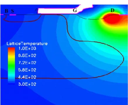
The Fig. 1.7 shows the cross-sectional schematic of the RESURF LDMOS under investigation. The device simulation data on the junction temperature profile within the LDNMOS during the snapback breakdown condition is shown in Fig. 1.8. It shows the N+/N- junction in the drain side has the maximum lattice temperature due to the Kirk effect [7]. Such a surface heat source is partially responsible for the ESD robustness.
Figure 1.7 The cross-sectional views of RESULF LDMOS [7].
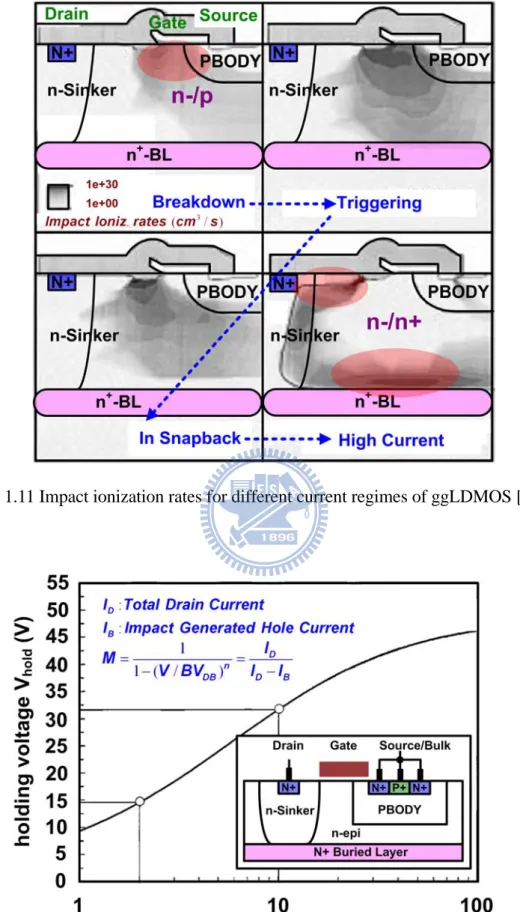
1.5 Investigation on the Impact of Kirk Effect to Holding Voltage [8]
The Figure 1.9 shows the typical I-V curves for different current regimes including the breakdown, BJT triggering, snapback and high current region after holding voltage in the ggLDMOS device. And the LDMOS device under investigation is shown in Fig. 1.10. After triggering of the parasitic BJT device, the strong source electron injection into the bulk results in a push-out of the depletion region across the lightly doped region of n-epi at the snapback state. The gradual progress of the avalanche impact ionization movement is depicted in Fig. 1.11. Apparently, the avalanche region eventually bumps into the highly n+ doped drain and buried layer diffusion in the high current region, which can generate much more electron-hole pairs. Hence, the impact generated hole are emitted and accumulated, which leads to a rapid increase of the hole concentration in the entire n-epi volume after turn-on of the parasitic BJT device. This effect is corroborated in Fig. 1.10, where the ratio of the avalanche hole nh to the n-epi donor doping concentration nd,epi depending on the
depth depi below the FOX is presented. The e-epi resistance and thus the on-resistance
is drastically reduced under the high current condition due to the large hole concentration in the n-epi volume. On the other hand, the current path widening is visible at high current region in Fig. 1.10. This effect also contributes to the low on-resistance after the ignition of the parasitic BJT.
The conductivity modulation of the n-epi due to the avalanche hole injection as well as widening of the current path within the large n-epi area lead to the transition from the high resistive breakdown regime to the low on-resistance of the high current region, as shown in Fig. 1.9.
Concluding, the extraordinarily low holding voltage after ignition of the parasitic BJT device can be attributed to three responsible mechanisms occurring in the BJT on-state [8]. One is the large avalanche multiplication factor at the holding state, and
other is reduced on-resistance and another is the large geometric extension of the avalanche region. Among the three parameters, the avalanche multiplication factor is dominant. The reduced on-resistance and the large geometric extension of the avalanche region have been analyzed as above. Now, the dependence of avalanche multiplication factor and the holding voltage is demonstrated in Fig. 1. 12. The large avalanche multiplication factor M is based upon an increase avalanche field. The field increase after triggering of the parasitic BJT is caused by the migration of the depletion region towards the highly doped drain n+ diffusion in contact with the n-epi which serves as a highly doped p+ diffusion due to the injection of the avalanche hole. The empirical Miller formula is used to describe the voltage V dependence of M, as shown in equation (1.1). The values of ID and IB represent the drain current and
impact generated hole current, respectively. Obviously, a lower holding voltage is attributed to the large avalanche multiplication factor, which can be accomplished by decreasing the n value and increasing IB.
(
)
1 1 / D n D B DB I M I I V BV = = − − (1.1)Besides, decreasing the k value can also reduce the holding voltage, as shown in Fig. 1.12. The k value represents the ratio of electrons reaching the drain to those that have undergone impact ionization, as shown in equation (1.2). It shows that almost all source emitted electrons reach the drain avalanche region and thus contribute to impact ionization.
.
.
Number of Drain Elect
k
Number of Multiplied Drain Elect
Figure 1.9 The I-V curves for different current regimes of ggLDNMOS: breakdown, BJT triggering, snapback and high current region after holding voltage [8].
Figure 1.10 Minority carriers (avalanche hole) injection into the n-epi depending on the depth perpendicular below the FOX (see inset) [8].
Figure 1.11 Impact ionization rates for different current regimes of ggLDMOS [8].
1.6 Brief Summary
The more and more extensive use of high-voltage (HV) technology in field applications such as automotive electronics and display driver ICs under demanding environments like high operating temperature and voltage requires very specific and appropriate protection against electrostatic discharge (ESD). As a result, ESD protection has become an important task on the reliability of HV ICs.
The LDNMOS transistor is most used in HV technology. However, using the parasitic NPN mode of the LDNMOS for HV ESD protection is not suitable due to the poor ESD robustness and low holding voltage. The poor ESD robustness is resulted from the non-uniform issue. And the low holding caused by Kirk effect leads to severe latch-up issue.
Among the ESD protection devices in HV technology, the SCR device is attractive and indispensable due to its superior voltage clamping capability, high failure current, high conductance and high area efficiency during an ESD event. However, the characteristics of high trigger voltage and low snapback holding voltage limit the ESD protection capability of SCR devices especially in HV technology. Thus, the trigger and holding voltage of SCR devices needs to be engineered to maximize the ESD performance.
In HV technology, the characteristic of extraordinarily low holding voltage will cause SCR devices susceptible to the latch-up danger in the real system applications, especially while those devices are used in the power-rail ESD clamp circuit. The extremely low holding voltage is related to the impact ionization occurring at the highly-doped junction due to Kirk effect. Thus, the SCR device for ESD protection in HV ICs is challenging due to the requirement of high latch-up immunity to minimize the risk of ESD-induced latch-up and electrical overstress.
Chapter 2
Prior Designs of Latch-up Immunity Increase
2.1 Holding Voltage Increase by Segmented Emitter Topology [9]
Electrostatic discharge (ESD) protections for high-voltage integrated circuits is developed to minimize the risk of ESD-induced latch-up threat by increasing the holding voltage of novel SCR structure larger than the power supply voltage. The SCR is designed based on the concept that the holding voltage can be increased by reducing the emitter injection efficiency accomplished by a segmented emitter topology in the SCR.
The cross-sectional view of triple-well SCR structure is shown in Fig. 2.1 and was fabricated in the BiCMOS 0.6-µm technology. The D5 and D6 in Fig. 2.1 define the base width and collector resistance in each bipolar transistor. A novel segmented topology is proposed and shown in Fig. 2.2. In the traditional configuration, the emitter N+ blocks in the cathode and emitter P+ blocks in the anode are continuous. In the novel segmented configuration, the emitter N+ and P+ blocks are not continuous and are separated by the well-tie blocks.
(a) (b)
Figure 2.2 The top views of SCR with (a) traditional stripe topology and (b) novel segmented topology.
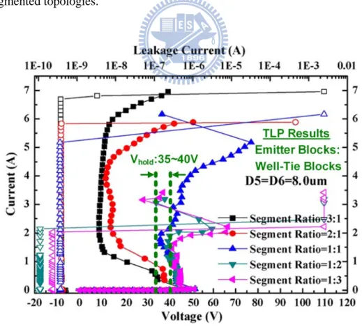
Fig. 2.3 shows the TLP-measured I-V curves of two SCR devices having the same width of 186µm and segment ratio of 1:1 but different topologies. The segment ratio is defined as the number of emitter blocks versus well-tie blocks. Clearly, the holding voltage has been increased significantly from 4V to 40V when the segmented topology is used. Note that the segmented DVR possesses a slightly higher trigger voltage and current due to the decrease in the well resistance by increasing the number of well ties in the device.
The different segment ratios affect the SCR’s holding voltage and can be seen in the TLP-measured results shown in Fig. 2.4. Obviously, decreasing the segment ratio further does not increase the holding voltage. And the failure current It2
decreases with decreasing segment ratio. The poor ESD robustness can be attributed to the current crowding resulting from the smaller emitter area. Nonetheless, a reasonably high It2 of 5.3A is still obtainable for the case of 1:1 segment ratio having a
Figure 2.3 The TLP-measured I-V characteristics for two SCR devices with the stripe and segmented topologies.
Figure 2.4 The TLP-measured I-V characteristics of SCR devices with different segment ratios and D5= D6= 8µm.
Figure 2.5 The TLP-measured I-V characteristics of SCR devices with 1:1 segment ratio having four D5/ D6 lengths.
Changing the dimensions of D5 and D6 can also alter the ESD performance. Fig. 2.5 shows the TLP-measured I-V characteristics of SCR devices with 1:1 segment ratio having four different D5= D6 dimensions. When D5= D6 is increased from 2 to 8µm, the holding voltage is increased from 10 to 45V due to the larger base width and collector resistance.
A new SCR structure has been developed and realized for high-voltage ESD applications. A higher holding voltage is developed based on the use of a segmented topology to reduce the emitter injection efficiency of the parasitic BJTs in the SCR. Besides, increasing the base width and collector resistance can also increase the holding voltage. Finally, a large holding voltage for latch-up immunity and high failure current for ESD robustness are accomplished and successfully verified in the 0.6-µm BiCMOS technology.
2.2 Holding Voltage Increase by Stacked Configuration Topology [10]
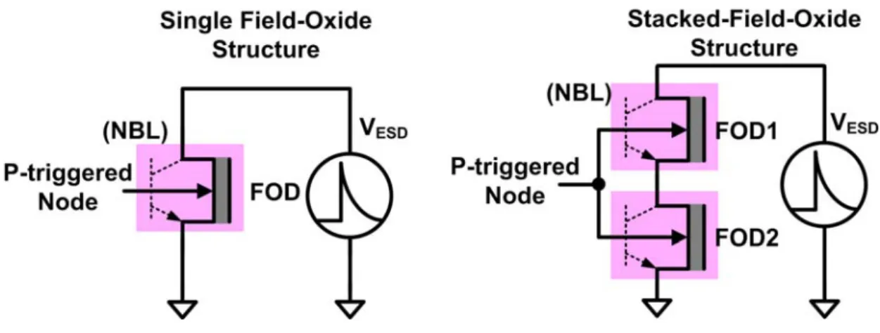
For high-voltage field-oxide (FOD) device structure shown in Fig. 2.6, the device is isolated by the n+ buried layer (NBL) from the p-type substrate. The spacing from collector diffusion to emitter diffusion of FOD device is 6µm.
Figure 2.6 The cross-sectional view of high-voltage field-oxide (FOD) device.
The measurement setup of single FOD device and stacked FOD device under TLP stress is shown in Fig. 2.7. The TLP-measured I-V characteristics of these devices with different device widths are compared in Fig. 2.8. The holding voltage of stacked FOD device in snapback breakdown region is double of that of single FOD device from the TLP-measured results. In addition, the It2 of stacked FOD device is only slightly
degraded as compared with that of single FOD device and can be adjusted by the variations of the device channel width. Obviously, the It2 of stacked FOD device is
linearly increased while the device channel width increases. Therefore, the required ESD robustness of stacked FOD device can be realized to sustain typical 2-kV (It2~1.33A) HBM ESD stress by adjusting the device width.
Figure 2.7 The measurement setup of single high-voltage FOD device and stacked-field-oxide structure under TLP stress.
Figure 2.8 The TLP-measured I-V characteristics of single FOD and stacked FOD devices with different device widths. W1 is the channel width of FOD1, and W2 is the channel width of FOD2.
However, the trigger voltage of stacked FOD device is also increased as compared with that of single FOD device. The substrate-triggered technique can be applied to lower the trigger voltage of the device to ensure effective ESD protection. The TLP-measured I-V characteristic of the stacked FOD device with different substrate-triggered currents (Itrig) is shown in Fig. 2.9. From the results, the trigger
voltage of the stacked FOD device can be decreased while the substrate-triggered is increased. The trigger voltage can be reduces from 40V to 17V when the substrate-triggered is 10 mA. Therefore, the trigger voltage of the stacked FOD device can be effectively reduced lower than that of internal circuits by substrate-triggered technique. Moreover, the It2 level of the stacked FOD device with substrate-triggered
current can be improved.
Figure 2.9 The TLP-measured I-V characteristics of the stacked FOD devices with different substrate-triggered currents.
Figure 2.10 Measurement setup for TLU test.
Transient-induced latch-up (TLU) test is used to investigate the susceptibility of the ESD protection devices to the noise transient or glitch on the power lines during normal circuit operating condition. The measurement setup for TLU test is shown in Fig. 2.10. The positive and negative charging voltage (Vcharge) on the energy storage
capacitor generating the transient is used to trigger the device into the latch state. A supply voltage of 40V was used and trigger source was connected directly to the device-under-test (DUT). The small resistance is used to protect the DUT when the DUT is triggered on into the latch state. In addition, the diode is used to avoid the damage to the power supply during TLU test. The voltage waveform on the DUT (at Y node) under TLU test is monitored in this experiment. The measured voltage waveforms on high-voltage stacked FOD device under TLU test with transient positive charging voltage and negative charging voltage are shown in Fig. 2.11.
(a)
(b)
Figure 2.11 The measured waveforms on the stacked-field-oxide structure under TLU test with (a) positive charging voltage and (b) negative charging voltage.
From the measured results, the device is initially kept off before the transient trigger, therefore the voltage waveforms are kept at 40V. After the transient triggering with the capacitor charging voltages of 80V or -50V, the stacked FOD is triggered. However, the clamped voltage waveforms quickly come back to the original supply voltage level of 40V, without keeping in the latch state. Hence, no latch-up issue is occurred. In addition, a higher capacitor charging voltage is needed to trigger on the stacked FOD device during the TLU test. As a result, the latch-up immunity of the stacked FOD device to the noise transient on the power lines in high-voltage CMOS ICs has been significantly increased.
Latch-up issue of ESD protection devices in high-voltage CMOS ICs has been clearly investigated by TLP stress and TLU test. By adjusting different numbers and different device channel widths of stacked FOD device, the total holding voltage can be designed higher than the supply voltage with the degradation of It2. As a result, a
new latchup-free power-rail ESD clamp circuit with stacked FOD device has been designed and successfully verified in a 0.25-µm 40-V CMOS process to meet the desired ESD level.
2.3 Holding Voltage Increase by Gate-Controllable Topology [11]
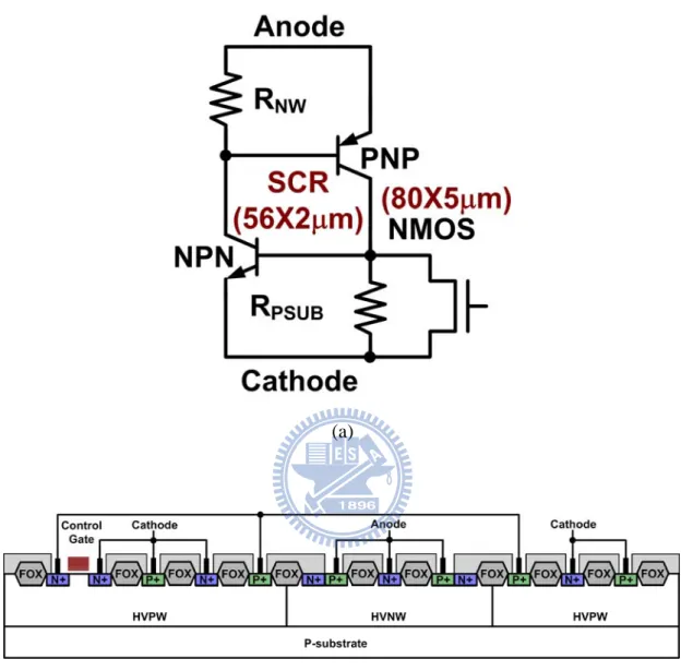
In this work, a simple gate-controllable high-voltage silicon-controlled rectifier (GC-HVSCR) is proposed in a 0.5-µm high-voltage (30V) CMOS process. The cross-sectional view and equivalent circuit of the GC-HVSCR are shown in Fig. 2.12. The HVSCR has a total width of 56x2µm and the control nMOS has a total width of 80x5µm.
The holding voltage (Vh) and the trigger voltage (Vt1) of the GC-HVSCR can be
adjusted by controlling the gate voltage of the nMOS. The simulated 2-D current flow lines of the GC-HVSCR under normal circuit operating and ESD stress conditions are
shown in Fig. 2.13. Under normal circuit operating condition, the gate of the control nMOS is biased with the supply voltage (30V). In Fig. 2.13(a), the current flow lines come from the anode to the P+ doped region. Under the ESD stress condition, the nMOS is set for the OFF state. In Fig. 2.13(b), the current flow lines come from the anode, through the N-well (NW) and the P-substrate, and finally to the cathode. The I-V characteristics of GC-HVSCR are sufficiently different under the normal circuit operating condition and ESD stress condition, which can be attributed to the different current flow lines.
From the simulated results in Fig. 2.14 (a), the breakdown voltage (VBV), trigger
voltage (Vt1) and holding voltage (Vh) under normal circuit operating condition are
40.7V, 69.8V and 55V, respectively. Under ESD stress condition, the breakdown voltage (VBV), trigger voltage (Vt1) and holding voltage (Vh) drop to 41.4V, 48.3V
and 2V, respectively. With the lower Vt1 and Vh, the overstress ESD pulse can be
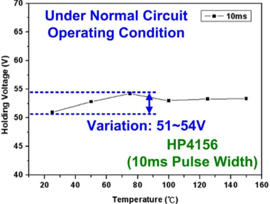
effectively clamped by the GC-HVSCR to protect the internal circuits against ESD damage. The TLP-measured I-V characteristics of GC-HVSCR under the normal circuit operating condition and ESD stress condition are shown in Fig. 2.14 (b). The holding voltages are quite different under the normal circuit operating condition and ESD stress condition. Under normal circuit operating condition, the holding voltage can be boosted due to the serial conduction path of the gate-controllable nMOS and PNP BJT. Therefore, the holding voltage of the GC-HVSCR can be raised to be greater than the supply voltage. When the nMOS is switched OFF under ESD stress condition, the holding voltage of GC-HVSCR can be reduced, thus providing efficient ESD protection. Besides, the overall temperature coefficient of the holding voltage in Fig. 2.15 is observed to be positive. As shown in Fig. 2.15, the holding voltage slightly varies between 51V and 54V for the temperature range from 25℃ to 125℃.
nMOS, whose temperature coefficients are of opposite signs and different amplitudes under normal circuit operating condition.
(a)
(b)
Figure 2.12 The (a) equivalent circuit and (b) cross-sectional view of the GC-HVSCR device.
The proposed GC-HVSCR device has been successfully verified in a 0.5-µm/30V CMOS process. From the simulated and experimental results, the Vh of GC-HVSCR
can be adjusted by changing the gate bias of the integrated control nMOS. The design is useful to avoid latch-up during normal circuit operating condition and at the same time offer high protecting performance under ESD stress condition.
(a)
(b)
Figure 2.13 The simulated 2-D current flow lines of the GC-HVSCR under (a) normal circuit operating and (b) ESD stress conditions.
(a)
(b)
Figure 2.14 The TLP-measured I-V characteristics of the GC-HVSCR under (a) normal circuit operating and (b) ESD stress conditions.
Figure 2.15 Measurement of the temperature dependence of the holding voltage of GC-HVSCR under normal circuit operating condition.
2.4 Holding Voltage Increase by Implantation of N-Buried Layer [12]
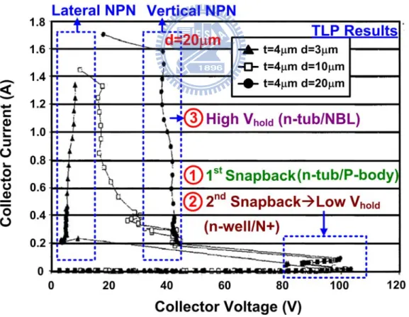
The variations of trigger and holding voltages are demonstrated in this work. The cross-sectional view of the NPN bipolar transistor is shown in Fig. 2. 16. In order to control the ESD parameters, two main layout parameters are varied, as shown in Fig. 2. 16. The parameters t and d are the distance between the p-body and n-well and the distance between the p-body edges to the n+ emitter, respectively. From Fig. 2.17, the I-V characteristics measured by TLP for this d array shows that d value influences strongly the holding voltage of the device. As d becomes large, the holding voltage increases. Indeed, increasing d enlarges the base width of the lateral bipolar while for the vertical bipolar the base width remains constant (process dependent). However for the vertical bipolar when d increases, the path in the BLN are longer and the additional distance represents low BLN collector resistance. Therefore, when d
switches off and the vertical bipolar takes the current. This shows that the current is now mainly flowing vertically via the BLN.
Figure 2.16 The cross-sectional view of the NPN bipolar transistor.
Figure 2.17 The TLP-measured I-V characteristics of the NPN bipolar transistor under different d values.
Besides, the values of small d, medium d and large d are simulated to further investigate the mechanism of holding voltage of the NPN devices. Figure 2.18 shows the migrations of impact ionization region in the NPN bipolar transistor at different current levels. At higher voltage, when the hole-avalanche current in the base is high enough to build up 0.7V under the emitter, this junction becomes forward biased and electrons start to get injected in the base. Because of this new source of electrons, the device may support the same current at a lower voltage and the first electrical snapback occurs. At that moment, a lateral bipolar turns on but the device is still in a low-current bipolar mode. The impact ionization region is still located at the p-body/n-tub junction, as shown in Fig. 2.18 (a).
When the current further increases, the base push-out effect arises. This effect appears when the mobile charge density at the depletion region of the base-collector region becomes higher than the fixed charge density. It results in an extension of the base into the n-tub, by which the ionization region is pushed away from the p-body/n-tub junction towards the collector n-well/n+, as shown in Fig. 2.18 (b). In these higher doped regions, the multiplication rate is higher, so a lower electric field is enough to obtain the same avalanche current. The voltage then drops to bring the device in a second strong and purely electrical snapback state. Therefore, this low holding voltage is thus related to the extremely high impact ionization occurring at the n+ collector regions.
If d is increased to 20µm, the vertical bipolar takes the current. Therefore, the base push-out occurs in the vertical direction pushing the impact ionization towards the BLN, as shown in Fig. 2.18 (c). When the impact ionization region reaches the BLN-layer, a second snapback occurs since the BLN is much higher doped than the n-tub. But since the BLN doping level is lower and much more gradual than that of
experiment, as shown in Fig. 2.17. This explains why the holding voltage is much higher for the large d device than for the small d.
(a)
(b)
(c)
Figure 2.18 The migrations of impact ionization region in the NPN bipolar transistor at different current levels.
(a)
(b)
Figure 2.19 The (a) TLP-measured I-V characteristics for variations of the parameter t and (b) linear dependence on the parameter t and the breakdown and trigger voltages.
Besides, the trigger voltage can be varied by changing the parameter t. As shown in Fig. 2.19, the parameter t influences strongly the breakdown as well as the trigger voltages of the device. As t becomes large, the breakdown and trigger voltages increase. The reach-through effect between the p-body and the n-well leads to a local increase of the electric field and earlier breakdown.
In summary, by changing the parameter t, the trigger voltage can be varied. And the parameter d is aimed to control the holding voltage by changing the lateral base width. Therefore, the bipolar conduction path (vertical or lateral) can be selected by adjusting the lateral base width. Besides, the re-allocation of impact ionization region due to the Kirk effect also determines the holding voltage of the NPN transistors. The impact ionization region locates at different junction leads to the different values of holding voltage. In general, the impact ionization region locates at the highly-doped junction results in the sufficiently low holding voltage.
2.5 Trigger Current Increase by PMOS-Triggered HVSCR [13]
To enable SCR based power protection a number of issues should be solved. First, the SCR needs to be triggered into the low resistive mode. Secondly, the static trigger current and voltage for the SCR needs to be engineered to a high value to prevent unwanted triggering during normal operation. A PMOS-triggered HVSCR is developed to meet the above two requirements. The cross-sectional view of the PMOS-triggered HVSCR is shown in Fig. 2.20. The width of HVSCR is 56µm. To be an efficient HV ESD protection device, the optimized trigger element needs to be added to lower the trigger voltage of ESD protection device. To prevent NMOS degradation and non-uniformity issues, the optimal trigger element for HV SCR based protection is a PMOS device, as shown in Fig. 2.20. The PMOS trigger element shows an advantage over NMOS based triggering because the NMOS would create a
latch-up issue due to the low holding voltage in the parasitic bipolar conduction mode. HV PMOS transistor handles the low ESD stress currents. When the ESD stress current reaches 300mA, the SCR is triggered into a low ohmic conduction.
Figure 2.20 The equivalent circuit of PMOS-triggered HVSCR.
Besides, the trigger voltage can be tuned to the desired voltage by selecting an appropriate size of the PMOS trigger element, as shown in Fig. 2.21. Finally, a high trigger current of SCR by use of the PMOS as a trigger element is realized and successfully verified in a 0.5-µm 43-V CMOS process. Hence, the SCR device is still kept off under normal circuit operation condition.
(a)
(b)
2.6 Brief Summary
The holding voltage higher than power supply voltage has been developed and realized to enhance the latch-up immunity. In this thesis, four solutions to increase the holding voltage and one solution to increase the trigger current of SCR devices are explored.
A high holding voltage can be accomplished by segmented emitter topology, which leads to the poor emitter injection efficiency.
By use of stacked configuration of field-oxide (FOD) devices can also increase the holding voltage of the FOD devices. However, the trigger element is needed to decrease the trigger voltage lower than the breakdown voltages of internal circuits. Besides, changing the current flows by the gate-controllable nMOS can meet the different requirements under ESD stress condition and normal circuit operating condition. The nMOS is kept off under ESD stress condition and kept on under normal circuit operating condition. Hence, the high holding voltage can be designed to higher than the power supply voltage due to the serial conduction path of nMOS and PNP transistors.
Therefore, the n-buried layer can promote the conduction of vertical SCR and further increase the holding voltage.
Finally, the trigger current of SCR device can be increased to a certain level to prevent the unwanted triggering under normal circuit operating condition. A PMOS-triggered HVSCR is realized to meet the requirement because the PMOS does not suffer the strong snapback issue.
Chapter 3
Parameters Investigation on Holding Voltage of
SCR
3.1 Latch-up Immunity Considerations under Normal Circuit
Operating Condition
The holding voltage higher than power supply voltage has been realized to enhance the latch-up immunity. The higher holding voltage discussed in the previous sections are measured by the TLP system. However, the latch-up event is a reliability test with the time duration longer than millisecond. TLP measurement is not suitable for applying to investigate the holding voltage of HV devices for latch-up immunity [14].
Fig. 3.1 shows the solutions to enhance the latch-up immunity. One way is to increase the trigger or holding current of ESD protection devices above certain minimum latch-up triggered current, as shown is Fig. 3.1 (a) and (b), and the other way is to increase the holding voltage of ESD protection devices to be larger than the power supply voltage under normal circuit operating condition, as shown in Fig. 3.1 (c).
In this work, SCR device is adopted as the HV ESD protection device to explore the latch-up immunity under normal circuit operating condition. The holding voltage, holding current and trigger current measured by the dc curve tracer and the 100-ns transmission-line-pulsing (TLP) system are investigated in different structures of SCR devices. Besides, the high immunity against transient-induced latch-up is developed in the stacked configuration of SCR devices.
(a)
(b)
(c)
Figure 3.1 Solutions to enhance the latch-up immunity by (a) trigger current increase and (b) holding current increase and (c) holding voltage increase under normal circuit operating condition.
3.2 Investigation on Holding Voltage increase of HVSCR
The equivalent circuit and associated voltage drops of SCR device are shown in Fig. 3.2. The holding voltage of SCR device can be expressed as the equations (3.1) and (3.2) [15]. The RC, PNP and RC, NPN are the parasitic collector resistances of PNP
and NPN transistors, respectively. And the RB, PNP and RB, NPN are the parasitic base
resistances of PNP and NPN transistors, respectively. In Fig. 3.2, the VC, PNP voltage
drop is caused by the collector current times the collector resistance of PNP transistor. Similarly, the VC, NPN voltage drop is caused by the collector current times the
collector resistance of NPN transistor. According to the equations (3.1) and (3.2), the holding voltage of SCR device can be adjusted by changing the collector and base resistances, as shown in Fig. 3.3. The holding voltage of SCR device can be increased by increasing the collector resistances or decreasing the base resistances of PNP and NPN transistors.
, , , , , , , , , , , ,
1
hold EC PNP C PNP BE NPN B NPN C PNP EC PNP BE NPN B NPN C PNP EC PNP BE NPN B NPNV
V
V
V
R
R
V
V
R
R
V
V
R
=
+
+
⎛
+
⎞
=
+
⎜
⎜
⎟
⎟
⎝
⎠
⎛
⎞
=
+
⎜
⎜
+
⎟
⎟
⎝
⎠
(3.1) , , , , , , , , , , , ,1
hold CE NPN C NPN EB PNP B PNP C NPN CE NPN EB PNP B PNP C NPN CE NPN EB PNP B PNPV
V
V
V
R
R
V
V
R
R
V
V
R
=
+
+
⎛
+
⎞
=
+
⎜
⎜
⎟
⎟
⎝
⎠
⎛
⎞
=
+
⎜
⎜
+
⎟
⎟
⎝
⎠
(3.2)In Fig. 3.3, increasing the collector resistances of PNP and NPN transistors leads to higher access resistance of conduction, and thus increases the holding voltage of SCR device. And the other way to fulfill the high holding voltage of SCR device is to decrease the base resistances of PNP and NPN transistors, which can lead to the poor emitter injection efficiency of SCR device. In other words, the more free carriers are needed to forward bias the base-emitter junction when the base resistances decrease. As a result, the holding voltage across the anode and cathode should increase to maintain the conduction of SCR device.
(a) (b)
(c) (d)
Figure 3.3 The sketches of (a) increasing RC, PNP and (b) increasing RC, NPN and (C) decreasing RB, NPN and (d) decreasing RB, PNP to boost the holding voltage of SCR devices.
3.3 Investigation on the Engineering of Trigger and Holding Voltage
Increase of HV SCR
To be an efficient ESD protection device, the trigger and holding voltage of SCR device should be adjusted. Fig. 3.4 shows the engineering of trigger and holding voltages of the SCR device. The trigger and holding voltages of SCR device are controlled by inserting the circuits at the different positions.
Figure 3.4 The engineering of trigger and holding voltages of the SCR device.
The trigger voltage of SCR device can be reduced by injecting the current into the base of NPN transistor or ejecting the current out the base of PNP transistor. Therefore, the SCR device turns on when the base-emitter junctions of PNP and NPN transistors are forward biased.
(a)
(b)
Figure 3.5 The sketches of decreasing the base resistance of NPN transistor in SCR device by (a) the gate-controlled NMOS and (b) the base-controlled NPN transistor.
The holding voltage of SCR device can also be increased. One way is to add the circuits into the conduction path of SCR device, and the other way is to shunt the base resistances of PNP and NPN transistors. The purpose of shunting the base resistances of PNP and NPN transistors is to reduce the base resistances of PNP and NPN transistors. Fig. 3.5 shows that the base resistance of NPN transistor in SCR device is reduced by the gate-controlled NMOS or the base-controlled NPN transistor. And the voltage potential of the gate or the base should be well controlled. In other words, the NMOS or NPN transistors must turn on to shunt the base resistance of parasitic NPN transistor under the normal circuit operating condition. On the contrary, the NMOS or NPN transistors must turn off during an ESD event.
![Figure 1.9 The I-V curves for different current regimes of ggLDNMOS: breakdown, BJT triggering, snapback and high current region after holding voltage [8]](https://thumb-ap.123doks.com/thumbv2/9libinfo/8760991.208173/30.892.235.676.109.481/figure-different-ggldnmos-breakdown-triggering-snapback-current-voltage.webp)