A 60-GHz High-Gain, Low-Power, 3.7-dB Noise-Figure Low-Noise Amplifier in 90-nm CMOS
Hsin-Chih Kuo and Huey-Ru Chuang
Institute of Computer and Communication Engineering, Department of Electrical Engineering, National Cheng Kung University, Tainan, Taiwan, R.O.C.
[email protected] [email protected] Abstract — This paper presents a 60-GHz high-gain,
low-power, 3.7-dB noise-figure (NF), CMOS low-noise amplifier (LNA) fabricated with a 90-nm process. The CMOS LNA exhibited a two-stage cascode structure with a common-source buffer amplifier. To achieve a lower NF and to prevent poor linearity, an inter-stage noise matching inductor and a derivative superposition method were applied to the LNA design. A thin-film microstrip (TFMS) line was used for matching networks and all interconnections. The TFMS line consists of a top metal layer (M9) serving as the signal microstrip line and a bottom metal layer (M1) serving as the ground plane. The measurement results showed that the proposed LNA exhibited the best gain performance of 22 dB at 57.3 GHz and a minimum NF of 3.7 dB at 61 GHz. The input third-order intercept point was -13 dBm. Further, the proposed LNA dissipated a total power of 13.5 mW from a 1.5 V power supply.
Index Terms — 60-GHz, derivative superposition, low-noise amplifier (LNA), noise matching, thin-film microstrip (TFMS) line.
I. INTRODUCTION
In recent years, the V-band spectrum for wireless personal network (WPAN) applications has become of special interest owing to its bandwidth of approximately 7 GHz, centered around 60 GHz. A high-quality, millimeter-wave (MMW), low-noise amplifier (LNA) plays an important role in modern wireless communication systems. In order to realize low-cost integration of the baseband and the RF front-end on the same die, a complementary metal-oxide semiconductor (CMOS) technology is one of the most attractive solutions to implement a highly integrated systems-on-chip (SoC) for MMW communication applications.
In the case of the LNA design in MMW receivers, an amplifier with a multistage topology is generally adopted to increase the power gain. However, the DC power consumption of such an amplifier is relatively high [1]. A gate-inductive gain-peaking technique for the LNA design [2]
is an effective way to achieve high gain performance with low power. Unfortunately, a high gain amplifier suffers from poor linearity. To improve the linearity properties, [3]-[5] have been studied. However, in these works, high linearity and a low noise figure (NF) could not be achieved simultaneously.
In this paper, we present a 60-GHz, high-gain, low-power, 3.7-dB NF, CMOS LNA fabricated with a 90-nm process.
This LNA utilizes a gain-peaking technique to achieve a
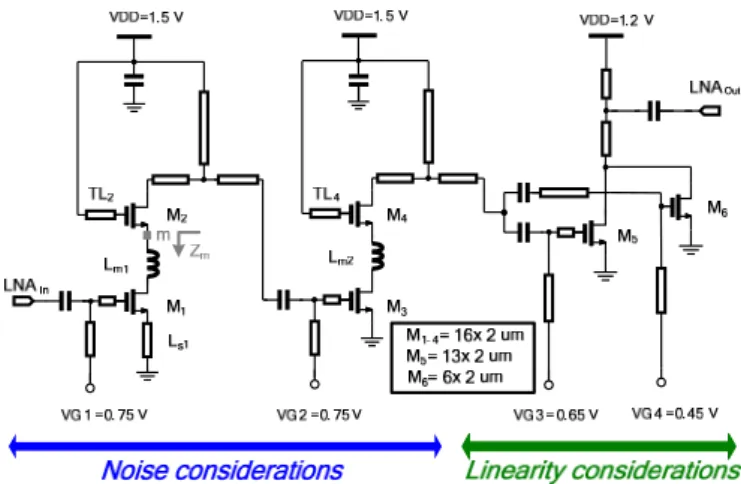
Fig. 1 Design concept and circuit schematic of the proposed 60-GHz high-gain, low-power CMOS LNA.
peak gain of 22 dB and a minimum NF of 3.7 dB while consuming 13.5 mW of power. Fig. 1 shows the design concept and circuit schematic of the proposed 60-GHz high-gain, low-power CMOS LNA.
II. LOW-NOISE AMPLIFIER DESIGN
Conventionally, the cascode stage is widely used for LNAs in a CMOS circuit design, owing to its better isolation and gain performance. In this study, a 2-stage cascode structure with a common-source (CS) buffer amplifier is adopted. The design tradeoffs between power gain and NF are considered for the first two stages. Therefore, the gate-inductive gain-peaking and the inter-stage noise inductor schemes are adopted in the first and second cascode amplifier stages to optimize the maximum available gain and the minimal NF.
The tradeoffs between the power gain and linearity are taken for the third stage. The third CS stage with a derivative superposition (DS) technique provides a tuning mechanism to prevent the process-voltage-temperature (PVT) variations.
On the basis of the noise considerations [6], the simulated current density of the 2-stage cascode structure was chosen as 156 μA/μm, and hence nMOS transistors (M1-4) with 16 fingers for the CS stage and the common-gate (CG) stage (each with W/L = 2 μm/0.1 μm per finger) were adopted. In addition, both the gate inductors Lg2 and Lg4 (denoted as TL2
and TL4, respectively) are in a transmission line structure.
0 0.1 0.2 0.3 0.4 0.5 0.6 0.7 0.8
Lm (nH) 3.5
4 4.5 5 5.5 6
Noise Figure (dB)
Ls = 0.05 nH Ls = 0.1 nH Ls = 0.15 nH Ls = 0.2 nH Ls = 0.25 nH Ls = 0.3 nH
0 10 20 30 40 50 60 70 80 90 100
Frequency (GHz) 0.14
0.16 0.18 0.2 0.22 0.24 0.26 0.28 0.3
L (nH)
2 4 6 8 10 12 14 16 18
Q factor
L Q
(a) (b) (c)
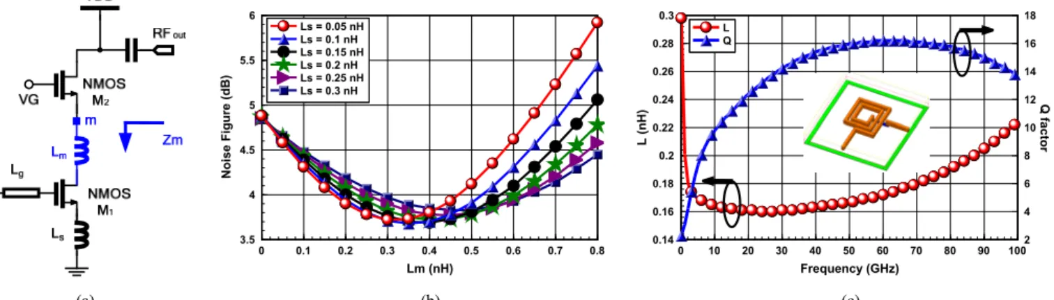
Fig. 2 Inter-stage noise matching inductor: (a) circuit schematic, (b) simulated NF for different Lm and Ls, and (c) simulated inductance and Q value of the TFMS line spiral inductor Lm.
A. Inter-stage noise matching inductor
As shown in Fig. 1, the thin-film microstrip (TFMS) line spiral inductors Lm1 and Lm2 were inserted in series with the signal path between the CS and the CG stages in each cascode structure for noise reduction considerations. The input impedance of the cascode structure from node m, also shown in Fig. 2(a), can be calculated as follows:
sds m s ds
m m
m m L
C g L SC
L I S
Z V
1 1 1
1
(1)
Eq. (1) describes the imaginary part of impedance Zm that depends on the inter-stage noise matching inductor Lm and the source degeneration inductor Ls. The imaginary part of impedance Zm can eliminate the effects due to parasitic capacitance. Thus, the parasitic resistance of the inductor will cause less noise than the original cascode cell. Fig. 2(b) depicts the NF versus different inductances of the Lm and Ls. It could be seen that the NF is reduced from 4.9 to 3.7 dB at 60 GHz by using the inter-stage noise matching inductor.
Furthermore, to achieve a compact size, the TFMS line spiral inductors are designed, which can provide a flexible layout routing. Fig. 2(c) shows the simulated inductance and Q of the TFMS line spiral inductor Lm. The optimal inductance and Q value are chosen as 170 pH and 16, respectively.
B. Linearity stage
The third CS stage with a DS structure is designed to prevent poor linearity. Generally, the third-order intercept point (IP3) of the n-stage cascaded system is expressed as follows:
2
3 , 3
12 12 2 3,2
12 2 3,1 2 3
1 1
IP IP
IP
IP A A A
A
(2)
Based on eq. (2), the cascode structure provides good isolation, owing to which the third linearity stage will not
affect the NF performance. Therefore, noise matching and high linearity performance can be achieved simultaneously.
All the requirements of inter-stage matching are implemented in the conjugate match to achieve maximum power transfer. The matching networks consist of series and shunt transmission lines that are implemented by 50-Ω TFMS lines. The TFMS line consists of a bottom metal layer (implemented by M1) serving as the ground plane and a top metal layer (by M9) serving as the microstrip signal line. The width of the TFMS lines is 9 µm, and the line-to-line distance for any pair of TFMS lines is more than three times the line width to avoid any mutual coupling effects. The TFMS line designs are based on the three-dimensional full-wave electromagnetic simulation by AnsoftTM HFSSTM.
III. MEASUREMENT RESULTS
The LNA was measured with on-wafer probing. The VDD supply voltage and total current consumption were 1.5 V and 9 mA, respectively. Because the parasitic effects of the RF pads were taken into consideration while performing the simulation, the measured results did not require de-embedding.
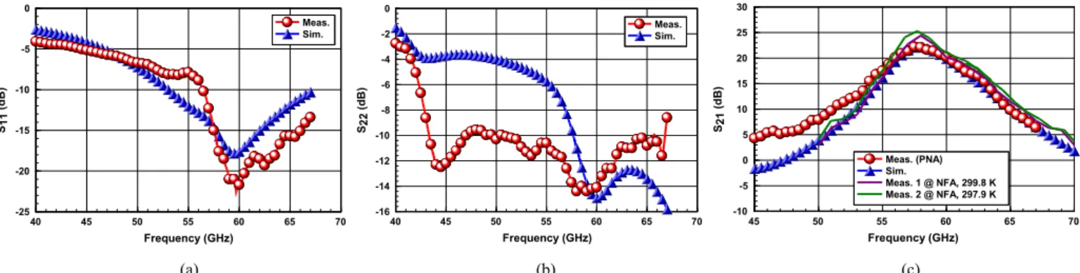
The measured input return losses (S11) and output return losses (S22) from 40 to 67 GHz are plotted in Figs. 3(a) and (b), respectively. From these figures, it is found that both the return losses are well below -10 dB over a frequency range of 57–64 GHz. The related stability K-factor is greater than 1.
Fig. 3(c) shows the measured peak power gain of 22 dB at 57.3 GHz. The simulated and the measured power gain are in good agreement with each other. Fig. 4(a) describes the NF measurement setup. We adopted two RF cables with different lengths (i.e., 60 cm and 120 cm) to verify the measurement (denote as Meas. 1 and Meas. 2). Two noise down-converters are used to cover the measurement frequency from 57 to 64 GHz. Fig. 4(b) shows the measured NF in the desired bandwidth are from 3.7 to 5.2 dB. The average NF is 4.3 dB.
Moreover, the gain performances measured by the noise figure analyzer (NFA) are also plotted in Fig. 3(c), which have a good agreement with the PNA's result. As shown in Fig. 5, the measured input 1-dB compression point (P1dB) and
40 45 50 55 60 65 70 Frequency (GHz)
-25 -20 -15 -10 -5 0
S11 (dB)
Meas.
Sim.
40 45 50 55 60 65 70
Frequency (GHz) -16
-14 -12 -10 -8 -6 -4 -2 0
S22 (dB)
Meas.
Sim.
45 50 55 60 65 70
Frequency (GHz) -10
-5 0 5 10 15 20 25 30
S21 (dB)
Meas. (PNA) Sim.
Meas. 1 @ NFA, 299.8 K Meas. 2 @ NFA, 297.9 K
(a) (b) (c) Fig. 3 Simulated and measured S-parameters: (a) input return losses (S11), (b) output return losses (S22), and (c) power gain (S21).
50 53 56 59 62 65
Frequency (GHz) 1
3 5 7 9 11 13
Noise figure (dB)
Sim.
Meas. 1 @ 60 cm, 299.8 K Meas. 2 @ 120 cm, 297.9 K
Min. NF=3.7 dB @ 61 GHz Avg. NF=4.3 dB
(a) (b) Fig. 4 NF measurement: (a) measurement setup and (b) simulated and measured results.
-40 -35 -30 -25 -20
Input Power (dBm) 12
13 14 15 16 17 18 19 20 21
Gain (dB)
-20 -18 -16 -14 -12 -10 -8 -6 -4 -2
Output Power (dBm)
Meas. Gain
Sim. Gain Meas. Output Power Sim. Output Power
1-dB Sim. Meas.
(a)
-40 -35 -30 -25 -20 -15 -10 -5
Input Power (dBm) -80
-70 -60 -50 -40 -30 -20 -10 0 10 20
Output Power (dBm)
Meas. Pout1 @ 60 GHz Meas. Pout3 @ 60 GHz Meas. Pout1 @ 60 GHz, Vg4=0.38V Meas. Pout3 @ 60 GHz, Vg4=0.38V
(b)
Fig. 5 Simulated and measured results for: (a) input P1dB and (b) input IP3.
Fig. 6 Chip micrograph.
the input IP3 of the amplifier are -23 dBm and -13 dBm at 60 GHz, respectively. Furthermore, Fig. 6 shows the LNA chip micrograph with a size of 0.76 × 0.78 mm2. Table I summarizes the performance comparison of our 60-GHz CMOS LNA with the reported LNAs, this work has an impressive NF and FOM performance.
IV. CONCLUSION
This paper presents a 60-GHz, high-gain, low-power, 3.7-dB NF, CMOS LNA fabricated with a 90-nm process. The proposed LNA adopted a two-stage cascode structure with a CS buffer amplifier. The proposed circuit achieves a peak gain of 22 dB at 57.3 GHz with a minimum NF of 3.7 dB; in
TABLE I PERFORMANCE COMPARISON
Ref. Tech.
(CMOS)
Supply Voltage
(V) Topology Gain
(dB)
IIP3 (dBm)
IP1dB
(dBm)
NFmin
(dB)
Powerdiss
(mW) FOM
[7]
2010 IMS 0.13 m 1.5 Current-reused 13.2 @ 58 GHz -4.7 -15 4.9 29.1 6.8
[8]
2011 MWCL 0.13 m 1.5 3-stage cascode 21 @ 53 GHz -16 -25 8.3 15.1 1.9
[9]
2011 RFIC 65 nm 1.2 3-stage cascade
(with T-Line) 20.6 @ 60 GHz N/A -29 4.9 @ 58 GHz 33.6 --
[10]
2012 RFIC 65 nm 1.25 3 CS TF + CF 23 @ 60 GHz ~ -16.5 -26.5 4 8 22.2
This Work 90 nm 1.5 2-stage cascode + 1 CS 22 @ 57.3 GHz -13 -23 3.7 @ 61 GHz 13.5 25.4
*
PDC NF
f IIP Gain
] FOM [
1 3
addition, input IP3 and input P1dB are -13 dBm and -23 dBm, respectively. Further, the total DC power consumed by the proposed circuit at 1.5 V is 13.5 mW. It should be noted that our proposed LNA has a lower NF, higher gain, and a higher figure of merit (FOM) than the reported state-of-the-art LNAs.
REFERENCES
[1] C. M. Lo, C. S. Lin, and H. Wang, “A miniature V-band 3-stage cascode LNA in 0.13 μm CMOS,” ISSCC Dig. Tech. Papers, pp.
322–323, Feb. 2006.
[2] Y. H. Yu, Y. S. Yang, and Y. J. E. Chen, “A compact wideband CMOS low noise amplifier with gain flatness enhancement,” IEEE J.
Solid-State Circuits, vol. 45, no. 3, pp. 502–508, Jan. 2010.
[3] V. Aparin, G. Brown, and L. E. Larson, “Linearization of CMOS LNA’s via optimum gate biasing,” in IEEE Int. Circuits Systems Symp., vol. IV, May 2004, pp. 748–751.
[4] B. Kim, J. S. Ko, and K. Lee, “A new linearization technique for MOSFET RF amplifier using multiple gated transistors,” IEEE Microw. Guided Wave Lett., vol. 10, no. 9, pp. 371–373, Sep. 2000.
[5] T. W. Kim, B. Kim and K. Lee, “Highly linear receiver front-end adopting MOSFET transconductance linearization by multiple gated transistors,” IEEE J. Solid-State Circuit, vol. 39, no. 1, pp. 223-229, Jan. 2004.
[6] T. Yao, M. Q. Gordon, K. K. W. Tang, K. H. K. Yau, M. T. Yang, P.
Schvan, and S. P. Voinigescu, “Algorithmic design of CMOS LNAs and Pas for 60-GHz radio,” IEEE J. Solid-State Circuits, vol. 42, no.
5, pp. 1044–1057, May. 2007.
[7] C. C. Chen, Y. S. Lin, J. F. Chang, and S. S. Lu, “A 4.9-dB NF 53.5-62-GHz micro-machined CMOS wideband LNA with small group-delay-variation,” IEEE MTT-S Int. Microw. Symp. Dig., vol. 2, pp. 489–492, Jun. 2010.
[8] C. C Huang, H. C. Kuo, T. H. Huang, and H. R. Chuang “Low-power, high-gain V-band CMOS low noise amplifier for microwave radiometer applications,” IEEE Microw. Wireless Compon. Lett. vol.
21, no. 2, pp. 104-106, Feb. 2011.
[9] H. H. Hsieh, P. Y. Wu, C. P. Jou, F. L. Hsueh, and G. W. Huang,
“60GHz high-gain low-noise amplifiers with a common-gate inductive feedback in 65nm CMOS,” in IEEE RFIC Symp. Dig., pp.
1–4, Jun. 2011.
[10] E. Cohen, S. Ravid, and D. Ritter, “A wideband gain-boosting 8mW LNA with 23dB gain and 4dB NF in 65nm CMOS process for 60 GHz applications,” in IEEE RFIC Symp. Dig., pp. 1–4, Jun. 2012.
![TABLE I P ERFORMANCE C OMPARISON Ref. Tech. (CMOS) Supply Voltage (V) Topology Gain (dB) IIP3 (dBm) IP 1dB (dBm) NF min(dB) Power diss(mW) FOM [7] 2010 IMS 0.13 m 1.5 Current-reused 13.2 @ 58 GHz -4.7 -15 4.9 29.1 6.8 [8] 2011 MWC](https://thumb-ap.123doks.com/thumbv2/9libinfo/9000118.285976/4.892.52.832.110.284/table-erformance-omparison-supply-voltage-topology-power-current.webp)
