國立台灣大學電機工程學研究所 碩士學位論文
D
EPARTMENT OFE
LECTRICALE
NGINEERINGC
OLLEGE OFE
LECTRICALE
NGINEERING ANDC
OMPUTERS
CIENCEN
ATIONALT
AIWANU
NIVERSITYM ASTER T HESIS
應用於外差式雷射干涉儀訊號之數位介面設計 A N EW D ESIGN OF D IGITAL I NTERFACE FOR
H ETERODYNE L ASER I NTERFEROMETER S IGNALS
官啟智 Chi-Chih Kuan
指導教授:蔡坤諭 博士 Advisor: Kuen-Yu Tsai, Ph.D.
中華民國九十七年七月
J
ULY, 2008
誌謝
在碩士班兩年的生活,首先我想感謝我的指導教授蔡坤諭老師,蔡老師在我的 研究上提供我很充沛的資源,並且對我學習的方向不會太過限制,很鼓勵我學習 不同領域的知識,在指導我研究方面也適時調整我的方向,讓我能順利完成碩士 的學習。我很感謝參與計畫的王倫老師與顏家鈺老師在計畫中提供我學習的機會 並容忍我許多犯錯的空間,另外我也很感謝在我研究上以及最後論文口試給我建 議的李佳翰老師與盧奕璋老師,以及提供我碩一和碩二研究環境的陳永耀老師。
感謝在碩班兩年陪伴我的好同學,期翔,信全,信宏,偉志,昭文,宇鋕,和 精密運動控制實驗室的凱翔,世康,黃璿,易道,傑方,有你們的陪伴讓我碩班 兩年遇到的痛苦被減輕,遇到的歡樂有你們在變得更歡樂,以及我的學長艮軒,
育諄,沛霖,孟福,水源,壹倫,孝天,致廷,志強,冠儒,你們給我的幫助和 歡笑我會牢記在心。
最後我要感謝我的父母和我的弟弟,感謝你們在這兩年來給我的鼓勵和安慰,
謝謝你們,以及我的女友盈鈺,感謝妳為我付出許多不為人知的辛酸,在我失敗 和落寞的時候妳和我的家人永遠是我最大的支柱。謝謝你們。
官啟智
中文摘要
由於對工具機及半導體步進機台精準度的嚴格要求日以遽增,相對來說對位移 感測器的要求日漸增加,雷射干涉儀是普遍用於位移量測的系統,其具有長距離 的量測範圍和低於奈米尺度的位移解析度。
在不同形式的雷射干涉儀中,外差式雷射干涉儀將光源等同於一個頻率的載 波,並將其用於偵測由移動的平台所產生的都普勒頻率與其對載波產生的頻率調 變,這項優點使外差式的雷射干涉儀相對於傳統的干涉儀不管是對外界環境或校 正誤差所產生的干擾都會有較好的抵抗力。
在這篇論文中首先會以邁克森雷射干涉儀作為開頭,接著介紹單調光雷射干涉 儀與外差式雷射干涉儀。在來介紹過去文獻中提出的幾種外差式雷射干涉儀介
面,以及此論文所提出的改良式的數位架構,最後將以邏輯閘的模擬和FPGA 的
驗證作為本篇論文的結束。
關鍵字: 外差式干涉法,相位量測,數位相位計,雷射量測系統,位移量測。
Abstract
Due to the rigorous demand on the precision of the manufacturing tools or the
lithography stepper, the request of the position sensor is also rigid. The laser
interferometer is the commonly used in the long range positioning system, and with
the sub-nanometer resolution.
In the laser interferometers, the heterodyne laser provides the light as frequency
carriers and catches the Doppler frequency from the moving stages in FM (frequency
modulation) mode. This benefit makes the heterodyne have good endurance to the
misalignment or other environment noise.
In this thesis, the first begins with the introduction of Michelson interferometer, the
homodyne interferometer, and the heterodyne type. The following are the prior digital
interfaces designed for the heterodyne laser interferometer, and the new modified
digital interface and architecture is proposed in this thesis. Finally, the gate-level
simulation and the FPGA verification are presented in the end of this thesis.
Keywords: heterodyne interferometry, phase measurement, digital phasemeter, laser measurement systems, displacement measurement
Statement of Contributions
General Contributions
The following are substantial achievements although not my original contributions.
1. Deliver a measurement system consisting of a Agilent N1231A interferometer
measurement board and a real time operating system implemented with
Mathworks xPC Target. It acquires the position data precisely for real-time
measurement.
2. Deliver an overall digital architecture for heterodyne laser interferometer.
3. Deliver a initial digital interface ASIC (application specific integrated circuit)
design for Agilent laser interferometer. It comes from following the CIC (Chip
Implementation Center) cell-based design flow to the gate-level simulation
without DFT insertion.
4. The above digital interface guarantees 10 nm displacement resolutions under the
pseudo measurement signal testing.
Original Contributions
The original contributions are as follow.
1. A new phase interpolation method for rising timing resolution is proposed. It
achieves 0.6 nm under on-chip testing.
2. A counter glitches canceling method is proposed and passes the verification on
gate-level simulation and FPGA on-chip testing.
Contents
誌謝... I 中文摘要... II
Abstract...III Statement of Contributions...IV Contents ...VI List of Figures ... VII List of Tables ...IX
Chapter 1 Introduction...1
1.1 Servo Control System ...1
1.2 Michelson Interferometer...2
1.3 Homodyne Laser Interferometer...4
1.4 Heterodyne Laser Interferometer...8
1.5 Homodyne and Heterodyne Comparison...11
Chapter 2 Electronics of Heterodyne Laser Interferometer ...14
2.1 Basic Operation...14
2.2 Delay Line Interpolator...16
2.3 Two-way Frequency-Conversion...18
2.4 Vernier Scale ...21
Chapter 3 Architecture...24
3.1 Octonary Phase Interpolation...24
3.2 Data path of Integer Part Calculation...25
3.3 Multiplexer Determination...27
3.4 Minimum Sorter Determination...29
3.5 Metastability and Displacement Resolution Discussion...31
3.6 Method comparison ...33
3.7 Gate Level Simulation on TSMC 0.18 μm Design Kits ...34
Chapter 4 FPGA Verification...42
4.1 Architecture Adapted for Cyclone III ...42
4.2 Gate-level Simulation and On-chip Testing...43
4.3 Optical System and Function Generator Testing ...52
Chapter 5 Conclusion and Future work ...59
References ...60
List of Figures
Figure 1.1 Servo Control Diagram...1
Figure 1.2 Schematics of Michelson Interferometer...2
Figure 1.3 Relationship of Phase Difference and Irradiance. ...4
Figure 1.4 Schematics of Homodyne Interferometer (Courtesy of Spindler and Hoyer Inc.) ...5
Figure 1.5 A simple signal processing circuit for homodyne interferometer. 8 Figure 1.6 Schematics of Homodyne Interferometer...9
Figure 1.7 Schematics of Heterodyne Interferometer (Courtesy of Spindler and Hoyer Inc.) ...11
Figure 1.8 Effect on homodyne misalignment...13
Figure 2.1 Basic Phase Estimation diagram. ...15
Figure 2.2 The block diagram of Zygo delay line interpolator. ...16
Figure 2.3 The operation diagram of Zygo delay line interpolator...17
Figure 2.4 Frequency conversion diagram...18
Figure 2.5 Two-way frequency conversion diagram. ...19
Figure 2.6 Phasemeters selection diagram...20
Figure 2.7 Mechanical Vernier Scale. ...20
Figure 2.8 The operation of Vernier scale method...21
Figure 3.1 The operation of Octonary phase interpolation. ...24
Figure 3.2 Fractional Part Determination. ...25
Figure 3.3 The control unit of the Integer part calculation. ...25
Figure 3.4 The save and reset timing diagram of the control unit. ...26
Figure 3.5 The integral parts counts change unstably...27
Figure 3.6 A counter module with save-and-reset control unit...27
Figure 3.7 count registers’ relationship with the fractional part value...28
Figure 3.8 Schematic of multiplexer determination. ...29
Figure 3.9 Schematic of minimum sorter determination ...30
Figure 3.10 Overall Architecture of the circuits. ...31
Figure 3.11 The probable determined phase location when the timing violation occurs...32
Figure 3.12 Gate-level Simulation in typical model...38
Figure 3.13 The details of the gate-level simulation results from 3D.7 to 39.3...39 Figure 3.14 The details of the gate-level simulation results from 39.3 to 36.0.
...40
Figure 3.15 (a) The gate-level simulation in fast model. (b) Gate-level simulation in slow model...41
Figure 4.1 Architecture adapted for Cyclone III FPGA...42
Figure 4.2 Gate-level Simulation on Cyclone III library...46
Figure 4.3 Testing diagram in Cyclone III FPGA...47
Figure 4.4 Diagram of SignalTap II Analyzer ...47
Figure 4.5 Testing the target mirror moves away from the interferometer. .48 Figure 4.6 Testing the target mirror moves close to the interferometer. ...49
Figure 4.7 RMSE comparison of the displacement difference in 11 different Doppler frequencies...51
Figure 4.8 The optical setup and the troubles in heterodyne laser source. ..52
Figure 4.9 The measured Doppler frequency when the target is stopped....53
Figure 4.10 The Doppler frequency result in a moving stage...54
Figure 4.11 The diagram of the function generator testing...55
Figure 4.12 The captured Doppler frequency in the function generator sweep mode...56
Figure 4.13 The function generator testing from -0.32 MHz to 0.8 MHz ...57
Figure 4.14 The function generator testing from -0.8 MHz to -0.48 MHz..58
Figure 4.15 The function generator testing RMSE in 11 different Doppler frequencies. ...58
List of Tables
Table 3.1 Comparison of Heterodyne Electronics ...34 Table 3.2 Testbench for gate-level simulation on TSMC 0.18 μm design kits.
...36 Table 3.3 Signal names for gate-level simulation on TSMC cell library...37 Table 4.1 Gate-level Simulation Environment for Cyclone III FPGA ...43 Table 4.2 Signal names for reference phasemeter on Cyclone III gate-level simulation...44
Chapter 1 Introduction
1.1 Servo Control System
In the past few years, computer numerical control machine has grown up rapidly.
The critical request to the information of position and velocity also grows up. Under
this framework, a high-precision discrete-time servo-mechanical system needs a
sensor to measure both position and velocity of the position stage in a real-time
manner. Most of sensors are realized as optical ruler or laser interferometer. The laser
interferometer has a benefit on long-range and high-resolution. This thesis chooses the
laser interferometer as a basis and develops electronic techniques to deal with the
stage position in high resolution and velocity tolerance.
Figure 1.1 Servo Control Diagram [1]
1.2 Michelson Interferometer
The basic and original concept of interferometers comes from Michelson
interferometer, which is shown in Figure 1.2. The coherent He-Ne Laser is incident
onto the non-polarized beam splitter and split into two light (1) and (2) which have
equal intense beam.
Laser
Counter
Concave Lens
Pin Hole Fixed Mirror
Translated Mirror
Interference Fringes
(1) (3)
(2)
x
Figure 1.2 Schematics of Michelson Interferometer [2]
The beam (2) hit the mirror which is fixed and the beam (1) hit the mirror which
translates with the stage or object under measured. The beam splitter combines the
reflection of them and redirects them into a concave lens. If we consider beam (1) and
beam (2) in time domain [3]:
1 0
2 0
cos( ) cos( ( ))
E E t
E E t t
ω ω θ
=
= + , where E0 is the wave amplitude of both beam (1) and beam (2). (1.1)
Then combine them as:
0 0
0
cos( ) cos( ( ))
1 1
2 cos( (2 ( ))) cos( ( ))
2 2
E E t E t t
E t t t
ω ω θ
ω θ θ
= + +
= + ×
(1.2)
0
2 cos(1 ( ))
E
=E
2θ t
(1.3)And the intensity read by photo detector is the square of amplitude:
2 2 2
0 2 0
4 cos (1 ( )) 2 2 cos( ( ))
E E t
E t
θ θ
=
=
(1.4)
The path lengths x can be represented as:
x λ
2θ
= ⋅
π
, whereλis the wavelength of laser source. (1.5)The path differences between beam (1) and beam (2) induce the phase change in
wave intensity, if the translated mirror continuously moves, the results behind the
concave lens is an annular fringe pattern and the sinusoidal intensity variation is read
by photo detector through the pinhole. The counter counts the integral multiples in
bright and dark fringes forλ /2 position resolutions. The advanced signal processing
technique in comparing relative phase through ADC achieves the resolution toλ /512
[4].
The thing that must pay attention is that the translated mirror must have a smooth
movement to reduce the back and forth vibration. The Michelson interferometer can
not afford acute back and forth vibration and will happen double counts of
interference fringes. It also needs a fine linear bearing to release this problem. To deal
with this issue and make the laser interferometry more unrestricted to environment or
equipment, the following improvement by generating quadrature outputs of
measurement signal is proposed and called homodyne laser interferometer.
Figure 1.3 Relationship of Phase Difference and Irradiance [3].
The reflection off the both mirrors will be partially incident onto the active volume
of laser source, as the beam (3) in Figure 1.2, the reflection may cause the external
resonate in the laser source, modulating the laser power and wavelength, to cope with
this problem, the corner cube mirror will be used to redirect the beam light and avoid
the overlapping in the laser source.
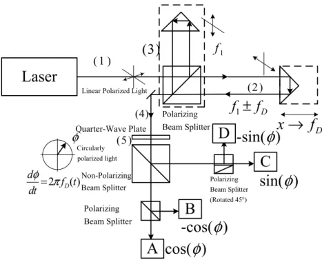
1.3 Homodyne Laser Interferometer
The homodyne interferometer schematic is shown in Figure 1.4. [5] The output of
laser source has been modified into the linear polarized beam and incident onto the
polarizing beam splitter, as mentioned foregoing, the homodyne interferometer
modify and rearrange the corner cube to replace the plane mirror in both fixed and
Laser
x → f
Df
11 D
f ± f
Polarizing Beam Splitter Quarter-Wave Plate
Non-Polarizing Beam Splitter
Polarizing Beam Splitter
Polarizing Beam Splitter (Rotated 45 )°
A
B
C D
( 1 )
(4)
(2 )
(3)
φ
(5 )2 D( )
d f t
dtφ π=
Linear Polarized Light
cos( ) φ -cos( ) φ
sin( ) φ -sin( ) φ
Circularly polarized light
Figure 1.4 Schematics of Homodyne Interferometer (Courtesy of Spindler and Hoyer Inc.)
The beam (1) is 45° with respect to beam (2) and beam (3), the beam (3) is incident
onto the fixed corner cube as the Michelson interferometer, and beam (2) is incident
onto the translated mirror and carry out the frequency
f modulated by Doppler effect,
Dwhich quantity is [5]:
2
D A
f v
=
λ
, whereλ
Ais the wavelength of laser source. (1.6)Both beam (2) and beam (3) is recombined as beam (4) in the polarizing beam
splitter and then redirected into the quarter-wave plate to transform into the circularly
polarized light. This optical setup also avoids the interference light incident onto the
laser source.
The optical setup before the beam (4) is very similar to Michelson interferometer,
after here, the beam (4) pass through a quarter-wave plate with its 45° linear
polarization, then transform into the circular polarization, and make the beam (5) have
180° phase differences in x and y direction, this phenomenon is used to generate
differential wave light for further purpose. The circularly polarized light has a phasor
which angular velocity is 2
π f
D. The rotating phasorφ
( )t
is the main object to be detected. To achieve this goal, the beam (4) is transferred through a polarizing beamsplitter and detected by photodetector A, the relationship between the laser intensity
and the signal A can be shown as [5]:
( ) ( ) [1 cos( ( ))];1 4
4 ( ) ( ) arccos[ -1]
( )
A O
A O
I t I t t
t I t
I t φ φ
= +
= ±
(1.7)
The ( )
I t is the intensity read from photodetector A, and the ( )
AI t is the intensity of
Olaser, which should be noticed that can fluctuate with time. By this equation, one
arccos value cause two ( )
φ t
which have opposite sign. This sign ambiguity can befixed by the quadrature signal generated from rotated 45° polarizing beam splitter.
( ) ( ) [1 sin( ( ))];1
C O 4
I t
=I t
+φ t
(1.8)The added sin term of ( )
φ t
helps classify the region[- /2, /2]π π
, accompany the arccos function, which region is [0, ]π
, the phasor located within [0,2 )π
can be determined. For implement issues, the aging laser source and optical components maycause the intensity ambiguity in the zero-crossing of the interference fringes. This
setup provides the complement signal of signal A and signal C as below:
( ) ( ) [1- cos( ( ))];1 4
( ) ( ) [1- sin( ( ))];1 4
B O
D O
I t I t t
I t I t t
φ φ
=
=
(1.9)
The beams which is incident to photodetector B and photodetector D comes from
another polarized light which have 180° phase differences to the original light. The
complementary signals can be regarded like differential signal pair represented as
digital data or as square wave converting in Figure 1.5. No matter the processing of
the complementary signals, it reduces the effects of intensity fluctuations on the phase
measurement.
Since the ( )
φ t
can be identified clearly, the velocity, v, and displacement, x, can be calculated as below:0
( ) ( )
( ) ( )
2 2 2 4
( )
A A A
D T
t t
v t f t
t x v t dt
λ ω λ φ λ
π π
= = = ∂
∂
=
∫
(1.10)
Note that the displacement x is measured up to time T.
Here shows a simple processing method deal with the homodyne interferometer. In
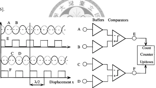
Figure 1.5 [7], the signals B and A are sent to a comparator and results the high/low
level voltage, so do signals C and D. The subtracting action reduces the ambiguity of
fringe contrast in zero-crossing, this low fringe contrast can appear from vibration,
interferometer mis-alignment and unequal in the non-polarizing beam splitter [5]. The
signal E and signal F are the outcome of two comparators, the signal E is the clock of
counter accumulate the register every positive edge trigger, and the signal F is the
up/down sign bit, when the signal E trigger, the bit F appeals low, that means the
displacement x is moving forward. Otherwise, if the bit F appeals high when the
signal E rising trigger, it means the reflector is translating backward. This method is
exquisite that combines both the optical phenomenon and digital techniques.
For further resolution, the xor operation can be applied to signals E and F to induce
double frequency, in this manner, the up/down sign bit must be attached to E&F
signal to occur a correct indicate. The more digital interpolation method is proposed
[6].
Figure 1.5 A simple signal processing circuit for homodyne interferometer.
1.4 Heterodyne Laser Interferometer
The heterodyne laser source generates the different frequency by several ways, and
two well-known manners are longitudinal Zeeman effect or acoustic optical
modulation (AOM) device [9].
As shown in equation (1.4), the photodetector amplitude is a cosine function of
phase differences ( )
θ t
between reference and measurement beam. The heterodyne can be viewed as a frequency shift in ( )θ t
:2 1
( ) 2
t
( - )f f t
'( )t
θ
=π
⋅ +θ
(1.11)Figure 1.6 [11] elaborates more clearly on heterodyne operation;
the
f
2-f frequency oscillates in a fixed frequency when the reflector stops ideally.
1The react Doppler frequency f
δ
from moving reflector makes the beat frequency shifting. What the digital interface that resolves the heterodyne operation needs to dois detecting every cycle’s frequency as precise as it can. To accumulate the detected
frequency and substrates the reference one can produce the phase '( )
θ t
that the phase difference results from the moving reflector.Figure 1.6 Schematics of Homodyne Interferometer
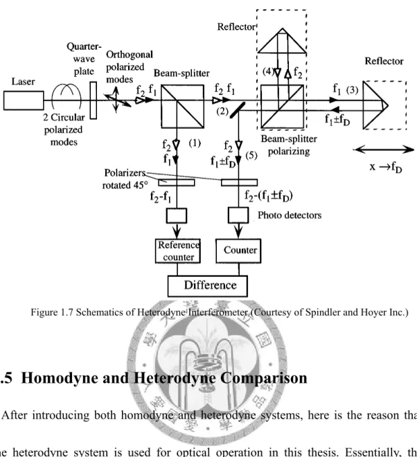
Heterodyne laser source outputs two frequency beams f1, f2, with circular
polarization as shown in Figure 1.7 [5], after passing through quarter-wave plate and
transforming into orthogonal polarized mode, the combinational two frequency wave
is incident onto a non-polarizing beam splitter for beam (1) and beam (2). Beam (1) is
directly incident onto a photodetector and feed through into a digital counter which
counts the cycle in one period of reference beam. Beam (2) carry on two frequency
with x and y direction polarization respectively. The polarizing beam-splitter separates
two different frequencies light. The beam which frequency is f2 enters a fixed
reflector, and the other one is incident onto the translated reflector, the induced
Doppler frequency here is fD, which is identical to equation (1.6). Two beams overlap
at beam (4) and feed into the photodetector. The counter counts and calculates the
time in one measurement signal cycle with a faster clock. The clock speed determines
the minimal timing resolution essentially. After both counters count reference and
measurement period respectively, the digital interface subtracts the measurement
value from the reference one. The difference can represent the phase variance in this
cycle. Accumulating the phase variance continuously, the displacement change can be
observed apparently.
Figure 1.7 Schematics of Heterodyne Interferometer (Courtesy of Spindler and Hoyer Inc.)
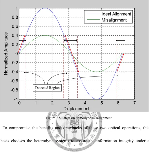
1.5 Homodyne and Heterodyne Comparison
After introducing both homodyne and heterodyne systems, here is the reason that
the heterodyne system is used for optical operation in this thesis. Essentially, the
homodyne system determines the intensity ratio of laser sourceI tO( ) and interference
fringes (For example,
I t in equation (1.7)). The homodyne is a method with a
A( )great potential because its resolution depends on ADC output bits [4] and without the
physical restriction in Doppler frequency, that means state-of-the-art electronics in
ADC or other mixed-signal circuits can help the improving in both position resolution
and velocity tolerance. But some realization problems may affect the signal integrity.
In realization, the intensity of bothI tO( )and ( )
I t must be in a stable range and the
Aphotodetector must have a good signal to noise ratio to keep the optical intensity
transferring to the electronic signal correctly. Besides, to setup a homodyne system
must challenge the following problem. (1) The measurement and reference beam
overlap changes during motion; this makes the optical alignment facing a critical
challenge or scarifies the coherence of interference fringes and loss the integrity in
displacement, as shown in Figure 1.8 [12]. (2) Non-ideal characteristics of
photodetectors, this may affect the intensity and produce the fault signal [12]. (3)
When doing the multi-axes measurement, the laser source intensityI tO( )must be
distributed to each axis equally; this makes the optical setup more complicated or
needs to use multiple laser sources to finish the multi-axes setup [12].
The heterodyne systems do not need the careful regard for the beam intensity. Since
the Doppler frequency fD is carried on light central frequency produced by either
Zeeman effect or AOM, the heterodyne systems care about the timing accuracy in
each measurement cycle. The heterodyne systems also have weakness in resolve the
displacement and velocity. To resolve the timing more accurate, the counting clock
frequency must be multiple times faster then the reference/central signal. The slow
reference frequency can have a better timing resolution intuitively, but the excessively
slow reference frequency will limit the target speed away from the photodetector,
which produces negative Doppler frequency.
0 1 2 3 4 5 6 7 -1
-0.8 -0.6 -0.4 -0.2 0 0.2 0.4 0.6 0.8 1
N o rm al iz ed A m pl itud e
Displacement
Ideal Alignment Misalignment
Figure 1.8 Effect on homodyne misalignment
To compromise the benefits and drawbacks of these two optical operations, this
thesis chooses the heterodyne systems to assure the information integrity under a
critical environment and inexpert optical alignment. Then increase the timing
resolution by digital circuits’ technique.
Chapter 2 Electronics of Heterodyne Laser Interferometer
2.1 Basic Operation
The basic phase estimation of heterodyne laser signal is to put on a counter and
count the cycle between the rising edges of measurement and reference signal, like the
T
1Δ in Figure 2.1 [14]. The phase change between cycles in Figure 2.1 isΔ
T
2-Δ ,T
1accumulates the phase change continuously, and the total phase displacement can be
determined. There still has problem in the determination ofΔ and
T
1 Δ , for example,T
2what if theΔ or
T
1 Δ is equal to 0? The control unit of the counter may have theT
2ambiguity whether it should reset the counter or not. The feasible method to estimate
the phase change is to place two counters to determine
T and
MT respectively, and
Rsubtract
T from
RT .Since
MT is almost a constant if the laser source frequency is stable
Renough, the interface updates the accumulating phase every rising edge of
measurement signal. The control unit will feel comfortable in this method and process
less error during the estimation of the phase variation.
Since the prototype of phase calculation is almost finished. There still has challenge
between the timing resolution and the limitation on the digital circuits. As discussed
before, the faster clock results the higher resolution on resolving every measurement
signal, but the digital counter can not afford the fast clock as higher resolution
expecting. Even the advanced lithography process progress everyday, the fast clock
also produces consideration power consumption and increase the chip temperature.
The following are several ways proposed to extend the timing resolution without
increasing the clock speed. In the following discussions, the integral part means the
multiple counts of the fast clock in Figure 2.1; the fraction part means the time
interval in one fast clock period that is determined.
T2 1 Δ
ΔT
1
1 360 360
R
T f N
ϕ = °ΔT = ° Δτ
TR
TM
Figure 2.1 Basic Phase Estimation diagram.
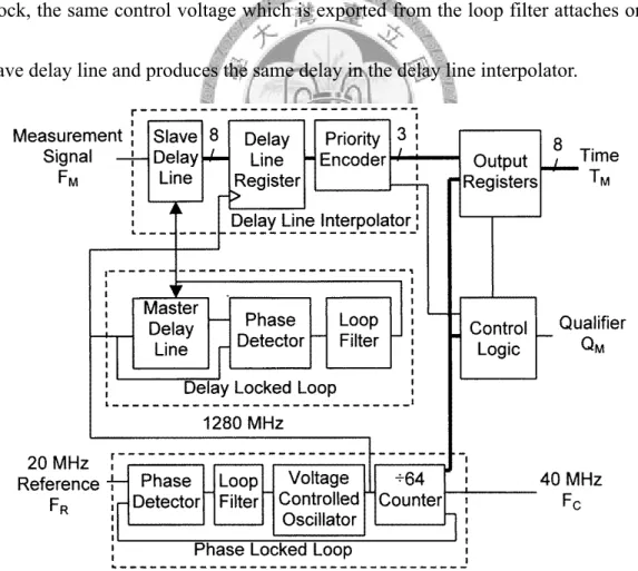
2.2 Delay Line Interpolator
The delay line interpolator method is proposed in 1998 by F.C. Demarest and Zygo
Corporation [15]. As shown in Figure 2.2, the fast clock is generated from PLL and 20
MHz reference signal FR. This PLL generates two clocks; one is 1280 MHz for the
counter to evaluate the integral part of the timing register, and the other is 40 MHz for
circuits processing. The 1280 MHz counter clock feeds into the delay locked loop
which has eight stages delay line. When the DLL lock the period of the 1280 MHz
clock, the same control voltage which is exported from the loop filter attaches on the
slave delay line and produces the same delay in the delay line interpolator.
Figure 2.2 The block diagram of Zygo delay line interpolator.
The slave delay line has the same delay behavior to the master delay line produced
by the master delay line. When the measurement signal enters into the delay
interpolator, the interpolator generates eight signals which have the delay to each
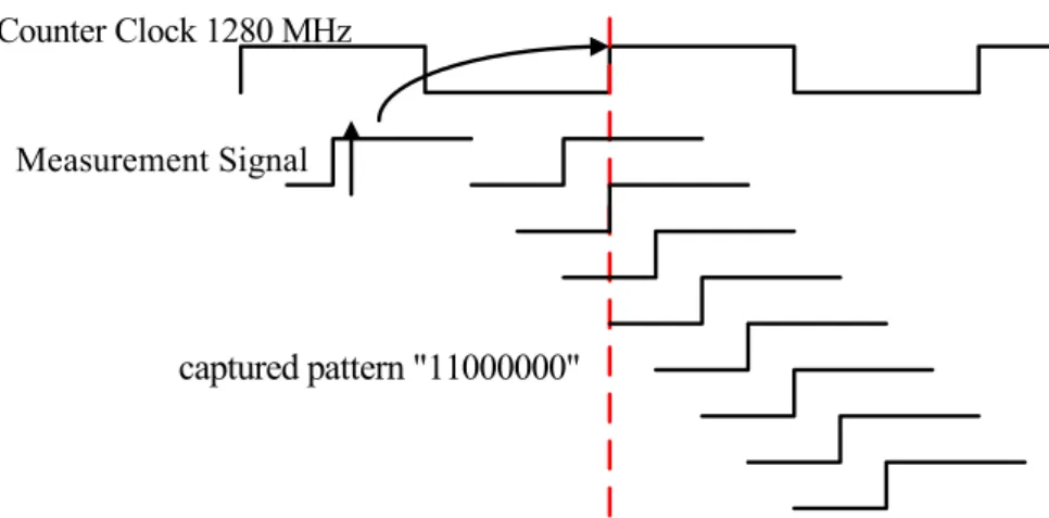
other in one of eight period of the counter clock. As shown in Figure 2.3 [16], when
the measurement signal occur a rising edge trigger, the control unit indicates the
counter clock to capture the output of delay line interpolator. The captured pattern can
represent the location where the measurement signal triggers in the previous counter
clock cycle. If the measurement clock is ideally close to the previous clock rising
edge trigger, the next clock trigger captures the pattern totally 1. And another situation,
if the clock triggers at just half of the clock period in the previous clock, the next
clock trigger will capture the pattern ‘11110000’. After the right code conversion, the
captured pattern can represent the fractional part in one clock period. By this skillful
method, it can obviously detect the timing under one clock cycle and have the eighth
resolution than just use the fast clock from PLL.
Counter Clock 1280 MHz
Measurement Signal
captured pattern "11000000"
Figure 2.3 The operation diagram of Zygo delay line interpolator.
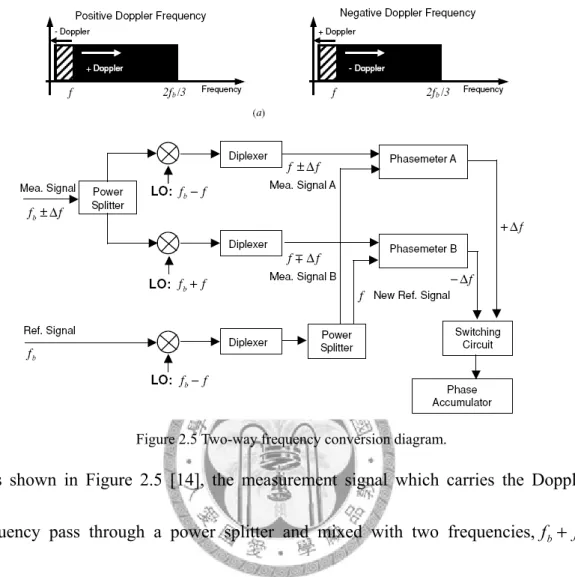
2.3 Two-way Frequency-Conversion
The homodyne technique has the problem in intensity and direction ambiguity, and
heterodyne technique has the restricted bandwidth by central frequency and resolution
specification. For example, the digital phase meter resolves the timing to 1ns; the
corresponding angular resolution is 0.36° in 1 MHz reference frequency. But the same
1ns, it only resolves to 3.6° in 10 MHz carrier signal. One way to increase the
resolution is to shift the measurement and reference signal in a lower level, as shown
in Figure 2.4 [14]. In Figure 2.4, the dropped heterodyne beat frequency
f causes the
bnarrow bandwidth in negative Doppler frequency.
The solution to this problem is to generate a signal which converts the Doppler
frequency to a contrary direction.
fb
Figure 2.4 Frequency conversion diagram.
As shown in Figure 2.5 [14], the measurement signal which carries the Doppler
frequency pass through a power splitter and mixed with two frequencies,
f
b+ ,f
and
f
b+ . The mixed signals have the identical carrier frequency f, and the Dopplerf
frequency fΔ have the same quantity but the opposite sign. The phasemeters digitalize
the Doppler frequency both fΔ and- fΔ . Since these dual frequencies can be detected,
Δf is obtained when fΔ is quite less than zero.
The converted Doppler frequencies have opposite sign in analog operation. A
switching circuit is used to select the right fΔ information. Shown in Figure 2.6 [14],
when the target has a positive velocity, the phasemeter A continuously unwrap the
information from the signal. When the velocity drops the zero, the phasemeter B starts
Figure 2.5 Two-way frequency conversion diagram.
to read the signal
and determines the fΔ . When the frequency is lower than -2/3f, which is the lowest
end that phasemeter A can detect, the switching circuit reads the data from phasemeter
B to phase accumulator to continue the unwrapping operation.
Figure 2.6 Phasemeters selection diagram.
(q r )
Y p L
M MN
= + +
Figure 2.7 Mechanical Vernier Scale.
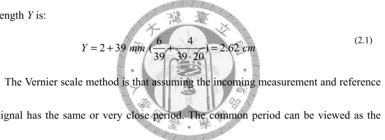
2.4 Vernier Scale
As its name, the Vernier scale method is developed from the mechanical Vernier
caliper [17]. Figure 2.7 shows the operation of the Vernier caliper. The unit length L is
divided into the equal segments which number is N and the stripes are inscribed on
the Vernier scale. The same length L in the main scale is divided into M divisions
(where M = cN – 1, c is a positive integer and is equal to 2 here). The resolution in
Figure 2.7 is L/(MN), and L in Figure 2.7 is 39 mm, M is 39, N is 20. The measured
length Y is:
The Vernier scale method is that assuming the incoming measurement and reference
signal has the same or very close period. The common period can be viewed as the
unit length L in the previous discussion. Pass the reference signal into a PLL and
multiply the frequency by M, so the generated clock has M divisions in one reference
6 4
2 39 ( ) 2.62
39 39 20
Y
= +mm
+ =cm
⋅
(2.1)
reference signal measurement signal
Main Clock
Vernier Clock
0 1
0 1 2 3
, 3 Lead the Main Clock Fractional Part is
1 Integral part is
Figure 2.8 The operation of Vernier scale method.
period. The measurement signal is passed through another PLL and generates another
clock which has N divisions in one measurement or nearly reference period. The
operation diagram is shown on. The main clock determines the integral part of the
phase difference. When the Vernier clock triggers, it begins to determine the fractional
part. Every Vernier clock period, the Vernier clock chases upon the main clock in
1/MN period of the reference signal [17]. The counts that Vernier clock chases is the
residual timing between the last main clocks trigger and the measurement signal
triggers in 1/MN resolution of the reference signal. In Figure 2.8 [17], the main clock
has the frequency M times that reference signal, and the Vernier clock has N times
than the measurement signal. The main clock begins to count the integral part when
the reference signal triggers. The counter counts to 1 when the measurement signal
comes up, so the integral part is 1/M. There still has time interval between the last
main clock triggers and the measurement signal rises. The following operation makes
the Vernier clock trigger detect the high low level of the main clock. Once the Vernier
clock overheads the main clock, it means the undetermined time interval of main
clock has been count in 1/MN (here the fractional part is 3/MN).
The Vernier scale method increases the resolution tremendously, but the lack of
velocity tolerance makes it difficult to realize on the servo control system. The reason
is that the moving target mirror affects both measurement signal and the Vernier clock
which is generated from the measurement signal and PLL. That means the moving
target mirror causes the jitter and undetermined timing during the fractional counting.
The previous research specify the restriction of the frequency deviation as the N times
of the Vernier clock, the vmax can be derived as below [18]:
The resolution is limited by the ts which is the settling time of the detecting flip-flop,
and the b can be estimated as b = ts
f
max, where the fmax is the maximum referencefrequency that the chip or device can work properly. This work is accomplished with
0.6 nm displacement resolution (with λ/2 linear interferometer), ± 0.3 m/sec target
speed.
2 max
( ) , where 1 2 ref
v f b b
N
≈
λ
= (2.2)Chapter 3 Architecture
3.1 Octonary Phase Interpolation
This method is the reverse of the Zygo delay line interpolator which delays the
measurement signal in one of eight of fast clock period. The PLL in this operation
generates eight phases’ signals of the fast clock. When the measurement signals
triggers, it outputs the pattern of these eight phase clocks’ high-low level, and if the
phases is generated precisely, the trigger location below one clock cycle can be
located in anyone of eight patterns in one clock period.
As shown in Figure 3.1. The measurement signal export the pattern from the eight
phase clocks. The 8-bits number then pass through a code converter and transform to
One clock period
"01111000"
Output pattern Measurement Signal
Eight Phase Clocks
a 3-bits number which represents the read phase location from 0 to 7.
Subtracting the previous measurement cycle’s phase location from the new read
ones induces the phase difference below one clock period between two measurement
cycles. This difference is employed as the fractional part of one measurement
counting, and expanding the timing determination sub clock.
3.2 Data path of Integer Part Calculation
The integer part time counting is to count the measurement signal period by a faster
clock, the counts can represent the time ought to the measurement signal period with
8 3 3
Phase Pattern
Phase Location
Subtractor
Fractional Part Counts 3
Figure 3.2 Fractional Part Determination.
Figure 3.3 The control unit of the Integer part calculation.
the timing resolution in one faster clock period. As shown in Figure 3.3, the idle state
is S_0, and when the measurement comes to 1, the state machine generates three
pulses sequentially, which first outputs counter’s value in that time, and then reset the
counter, finally outputs the fractional part value. When the measurement goes down to
0, the circuits accumulate the counts as the incremental phase difference. During the
pass and reset process, the circuits do not count the time even the measurement signal
is in high voltage level. Due to this situation, the real integer counts are the counter’s
counts plus 2.
In Figure 3.5, a trouble appears when the circuits are implemented on the FPGA.
Since the counts’ integral and fractional part is calculated separately. The
meta-stability problem of the integral part counter induces the value instability even
the frequency varies within one clock period. This problem drops the time resolution
to one clock period, and the fractional part detect is useless because the integral part
varies an extra count and the frequency do not change so. The following sections
propose several ideas to solve this problem and guarantee the time resolution under a
Figure 3.4 The save and reset timing diagram of the control unit.
clock period.
3.3 Multiplexer Determination
In previous sections, a counter module with save-and-reset action is represented as
an int_counter module as in Figure 3.6. Eight int_counter modules are employed and
connect with eight different phases of clocks, and each of them counts the same
measurement signal.
Figure 3.5 The integral parts counts change unstably.
Control Unit
Measurement Signal
Clock
Reset Counter
Counts Register
32 32
Output the counts
int_counter module
32 Measurement Signal
Clock
Figure 3.6 A counter module with save-and-reset control unit.
In ideal case, the output counts register has a corresponding relationship with the
fractional part value. As depicted in Figure 3.7, the count_reg_0 to
count_reg_7 are the counts result of eight different phase’s clock which count the
same measurement signal. The 3-bits sel register is the phase location of that cycle’s
measurement trigger. The sel here from 6, 5, to 4 in each measurement cycle, which
reveal the fractional part value is 7. In integral part, one of the eight numbers is 3D
and others seven are 3E. It means there are 7 clocks has triggered before the
measurement signal trigger in the last clock period. This multi-counter calculation
helps us to determine the integral part value more accurate. The first developed
method is to select the counts register by the multiplexer. As shown in Figure 3.7, the
correct register is count_reg_6 where the sel is 5. The less integral number plus
the fractional part constitute the correct frequency estimation. The schematic is shown
as Figure 3.8.
Figure 3.7 count registers’ relationship with the fractional part value.
Although the multiplexer selection looks reasonable, it gets tough to realize on chip.
This architecture can not endure different PVT library, and selection between the
phase location register sel and the correct integral register is mismatch under
different process library. Besides, under the FPGA test, the integral part still vibrates
no matter the register is choose. A revised integral part determination is proposed in
the following section to deal with this problem.
3.4 Minimum Sorter Determination
The multiplexer determination causes plenty of troubles in implementation; the
minimum determination is the improved function to choose the correct integral
register. As shown in Figure 3.7, the correct integral part value is 3D no matter the
Code Conversion
8 3 3
3 Clock[0]
int_counter_0
32 Measurement Signal
Clock[1]
int_counter_1
32 Measurement Signal
Clock[2]
int_counter_2
32 Measurement Signal
Clock[7]
int_counter_7
32 Measurement Signal
Mux
29Integral Part Counts
Fractional Part Counts Subtractor
Phase Location Phase Pattern
Figure 3.8 Schematic of multiplexer determination.
phase location is 6, 5, or 4, and the minimum of the eight integral part values also can
represent the counts from the last beginning clock after the measurement signal trigger.
This method endures the different process corner and performs a better result then the
foregoing. The further formation is to pass the signal into both minimum and
maximum minus 1 block, as shown in Figure 3.9. This arrangement is to prevent the
miscounting situation like in Figure 3.7 if the only minimum register is miscount to
3E. The fractional part is involved again to recognize which register should be
employed. The complete block diagram is shown in Figure 3.9.
The overall architecture is shown in Figure 3.10. The multiply 64 PLL generates the
eight phases’ clocks and synchronizes with the reference signal. The phasemeter
8 3 3
3
Figure 3.9 Schematic of minimum sorter determination
mentioned foregoing calculates the measurement count and outputs the digital words.
The adder adds the constant reference count due to the synchronized reference signal.
The variance between the measurement count and reference count can represent the
velocity output in the moment, and the incremental velocity is the accumulated
displacement since the measurement process starts.
3.5 Metastability and Displacement Resolution Discussion
In practical realization, it only needs four clocks in Figure 3.1 and is enough to
determine eight phase location where the measurement signal triggering. Assume that
the flip-flops’ setup and hold time region are not over eighth of one clock period.
As shown in Figure 3.11, the measurement signal triggers at the rising edge of clk1.
Since the clk2, clk3, and clk4 are stable in this region, the probable location here is
phase location 7 or 0, which is only affected by the metastability in clk1. However, no 64 PLL
×
Figure 3.10 Overall Architecture of the circuits.
matter which location is chosen, the displacement error does not exceed the resolution
that under eighth of one clock period.
The displacement resolution relies on the timing resolution of the reference signal
but not the measurement ones. If the fixed timing resolution is 0.1ns, the displacement
resolution is 0.632 nm if the wavelength is 632 nm and the frequency is 1 MHz. The
resolution rises to 63.2 nm if the frequency is up to 10 MHz. In the heterodyne
interferometry, the displacement resolution is the phase or timing resolution of the
reference signal. The measurement signal’s timing results only represent the time
portion in the reference one. Although the fixed timing resolution may have the more
indistinct resolution in resolving the fast measurement signal’s timing, the counted
measurement portions under the reference signal phase resolution does not affect or
drop the resolution of displacement.
One clock period
Figure 3.11 The probable determined phase location when the timing violation occurs.
3.6 Method comparison
The Zygo delay line interpolator has a good performance including the high
displacement resolution under a clock period and high velocity tolerance of target
mirror, but it requires more sophisticated analog components (one PLL, one DLL, and
one delay line) to cooperate and finishes the work. The frequency shift method has a
great advancement in displacement resolution and hold on the tolerance in mirror
translation velocity, but it also needs lots of analog component such as mixers,
diplexers, and frequency synthesizers to generate precise frequency in local oscillator
parts of Figure 2.5 [14]. The frequency of local oscillator needs the precise adjustment
or it makes error in calculating the displacement.
The Vernier scale method needs less analog components (two PLLs) to achieve high
displacement resolution. But the measurement signal induces the clock unstable
troubles and restricts the mirror translating speed to 0.3 m/s.
The self-developed octonary interpolator provides a digital architecture to solve this
problem with less analog components (one eight phase PLL), and make it easy to
implement entire measuring system in a FPGA board (Altera Cyclone III FPGA). The
following is the comparison of several heterodyne electronics.
Table 3.1 Comparison of Heterodyne Electronics
3.7 Gate Level Simulation on TSMC 0.18 μm Design Kits
To simulate and test the interferometer digital circuits, a method is to employee a
variable wave to simulate the effect of Doppler frequency. If the circuits can detect the
measurement frequency indeed, the variance between it and reference frequency can
be detected. Displacement and speed of the target mirror can also obtain.
The testbench sets the reference frequency as 4 MHz for Agilent Laser Head 5517D
which frequency ranges from 3 MHz to 4 MHz, and multiply the clock frequency up
to 256 MHz. Cooperating with the octonary phase interpolator, the total displacement
resolution compromises to λ/512, λ is the wavelength of laser and comes to 632 nm in
vacuum. The measurement frequency is set as a frequency variant signal, which varies
Mea. Sci.
1998
Mea. Sci.
2004
Mea. Tech.
2006
Agilent N1231B
This work
Position Resolution
λ/512 λ/1024 λ/512 λ/1024 Function generator testing:λ/64
On-chip PLL testing:
λ/512
Speed Tolerance in Target Mirror
2.2 m/s 2.4 m/s 0.3 m/s 2.8 m/s 0.5 m/s
Electronic Implementation
Digital:
ECL Asic.
Analog:
one DLL, one Delay Line one PLL.
Digital: FPGA Analog:
Mixers, Diplexers, Frequency Synthesizers
Digital:
FPGA Analog:
Two PLLs.
Digital: FPGA Analog:
Unknown.
Digital: FPGA Analog:
one PLL (8 phase output.)
measurement triggering, the frequency variance is set as a fractional number which
denominator is 512.
The testbench of this simulation and the detailed measurement profile is shown in
Table 3.2. As shown in Figure 3.13, the pictures show the circuits work properly
during every measurement frequency changes. Equation (3.1) shows the relationship
between the measurement period and the detected integral and fractional value. The
measurement period is modulated with (any value/512), which means the minimum
timing resolution under this architecture is 1/512 of reference period. The integral part
is determined by the counter which has clock speed 64 times than reference period.
The resolution of the integral part is 1/64 of reference period. The fractional part is the
eight phase interpolator of one clock period, which has 8 times timing resolution than
the clock speed, also as 1/512 of reference period time resolution.
( ) ( 2) ( )
512 64 512
ref ref
ref
T T
any value
T
× = ×Integral
+ +fractional
(3.1)Table 3.2 Testbench for gate-level simulation on TSMC 0.18 μm design kits.
The first simulation result is in typical model, as shown in Figure 3.12. Table 3.3
shows the signal index of each signal. The corresponding counts appears clearly with
the measurement frequency change even the variance is small. Figure 3.13 and Figure
3.14 are the zoom-in figures from Figure 3.12. The detailed signals like the state
machine are shown and the correct integral part can be determined without error. The
fractional part is also shown as predicted. Figure 3.15 shows the simulation results in
slow and fast model. During the simulation in slow model, most phase location cannot
be ascertained due to the timing violation between measurement trigger and the clocks
transition. It means the chip cannot work in the difficult environment or the mistakes
Library
TSMC 0.18 μmArea
870938.515625 μm2Clocks
Eight 256 MHz clockswith 45° difference
Displacement Resolution
λ/512Reference Frequency
4 MHzMeasurement Frequency
Period Corresponding Integral Value
Corresponding Fractional Value
250 ns * (511/512)
0x3D 7250 ns * (502/512)
0x3C 6250 ns * (493/512)
0x3B 5250 ns * (484/512)
0x3A 4250 ns * (475/512)
0x39 3250 ns * (466/512)
0x38 2250 ns * (457/512)
0x37 1250 ns * (448/512)
0x36 0typical model.
Mea_clk
Measurement Frequency.Clk[7:0]
Eight different phase clocks.Count_sub[31:0]
The value the subtract measurement counts from the reference counts.Count_reg
The selected integral parts by combination logicsCount_reg_0[31:0]
Integral parts of measurement countssynchronized with clk[0].
Count_reg_1[31:0]
Integral parts of measurement counts synchronized with clk[1].Count_reg_2[31:0]
Integral parts of measurement counts synchronized with clk[2].Count_reg_3[31:0]
Integral parts of measurement counts synchronized with clk[3].Count_reg_4[31:0]
Integral parts of measurement counts synchronized with clk[4].Count_reg_5[31:0]
Integral parts of measurement counts synchronized with clk[5].Count_reg_6[31:0]
Integral parts of measurement counts synchronized with clk[6].Count_reg_7[31:0]
Integral parts of measurement counts synchronized with clk[7].Fraction[2:0]
Fractional parts of measurement countsSel[2:0]
Phase Location of measurement triggerTotal_count[31:0]
Accumulated phase variance.Total_reset
Reset signal to total_count[31:0] register.Reg_transfer
State 1 of state machine to save the counters’ counts.reset
State 2 of state machine to reset the counters.(Negative trigger.)
Sel_ctrl
State 3 of state machine to shift previous and present phase location.(Negative trigger.)
add
Accumulate the phase difference.Table 3.3 Signal names for gate-level simulation on TSMC cell library
Corresponding Counts From 3D.7 to 3C.6
Corresponding Counts From 3C.6 to 3B.5
Corresponding Counts From 3B.5 to 3A.4
Corresponding Counts From 3A.4 to 39.3
Figure 3.13 The details of the gate-level simulation results from 3D.7 to 39.3.
Corresponding Counts From 39.3 to 38.2
Corresponding Counts From 38.2 to 37.1
Corresponding Counts From 37.1 to 36.0
(a) (b)
Figure 3.15 (a) The gate-level simulation in fast model. (b) Gate-level simulation in slow model.
Chapter 4 FPGA Verification
4.1 Architecture Adapted for Cyclone III
The PLL included in Cyclone III can not lock the input frequency under 4 MHz. To
compromise this situation, the architecture is modified to two phasemeter and
subtracts the measurement count from reference ones. The chip clocks run at 260
MHz and the displacement resolution is around λ/550. The overall architecture is
shown in Figure 4.1. Unlike the other one shown in Figure 3.10, this architecture
counts both reference and measurement signal simultaneously, and synchronizes the
reference count with the measurement part control signal. This setup synchronizes the
reference count which is updated by the reference signal, and avoids the timing
violation due to the different updating frequency.
Figure 4.1 Architecture adapted for Cyclone III FPGA
4.2 Gate-level Simulation and On-chip Testing
Before the experiment, the gate-level simulation provides a platform to verify whether
the design is workable. Here uses Altera® Cyclone® III library and Synopsys® Design
Compiler® for HDL synthesis and delay annotation. The clock speed drops to 32 MHz
due to the conservative delay model. The clock speed rises to 260 MHz on the on-chip
testing. The actual integral value is 8 here when the measurement frequency is equal
to reference frequency, but the calculated value is 6 here. The missed 2 is due to the
save and reset process in the state machine.
Table 4.1 Gate-level Simulation Environment for Cyclone III FPGA
Library
Cyclone IIIArea
N/AClocks
Eight 32 MHz clocks with 45° differenceDisplacement Resolution
λ/64Reference Frequency
4 MHzMeasurement Frequency
Period
Corresponding Integral Value Corresponding Fractional Value250 ns* (127/64)
0xD 7250 ns* (118/64)
0xC 6250 ns* (109/64)
0xB 5250 ns* (100/64)
0xA 4250 ns* (91/64)
0x9 3250 ns* (82/64)
0x8 2250 ns* (73/64)
0x7 1250 ns* (64/64)
0x6 0The following chart splits to two to show the signal index of the reference and
measurement timing diagram.
Table 4.2 Signal names for reference phasemeter on Cyclone III gate-level simulation.
ref_clk
Reference Frequency.Clk[7:0]
Eight different phase clocks.Count_reg_ref[31:0]
The selected integral parts of reference countsCount_reg_0[31:0]
Integral parts of reference countssynchronized with clk[0].
Count_reg_1[31:0]
Integral parts of reference counts synchronized with clk[1].Count_reg_2[31:0]
Integral parts of reference counts synchronized with clk[2].Count_reg_3[31:0]
Integral parts of reference counts synchronized with clk[3].Count_reg_4[31:0]
Integral parts of reference counts synchronized with clk[4].Count_reg_5[31:0]
Integral parts of reference counts synchronized with clk[5].Count_reg_6[31:0]
Integral parts of reference counts synchronized with clk[6].Count_reg_7[31:0]
Integral parts of reference counts synchronized with clk[7].Fraction[2:0]
Fractional parts of reference countsSel[2:0]
Phase Location of reference signal triggerReg_transfer
State 1 of state machine to save the counters’ counts.reset
State 2 of state machine to reset the counters.(Negative trigger.)
Sel_ctrl
State 3 of state machine to shift previous and present phase location.(Negative trigger.)
add
State 0 of state machine to process the integral part counts determination.The timing diagram shown in Figure 4.2 shows the reaction of the output registers
after the measurement signal in Table 4.1 is fed in. The selected integral part value
varies depending on the different measurement signal, and the fractional part also
responds as expecting. The signal index of the Figure 4.2 (a) is same as the Table 3.3.
Although the reference integral part count is less 2 than the actual value which should
be detected, the measurement ones suffer the same situation. After the subtraction for
the frequency determination, the non-ideal issue is canceled and output the correct
frequency information.
As shown in Figure 4.3, the on-chip testing employees a PLL to simulate the variant
measurement frequency. The two PLLs on Cyclone III chip connects to two different
oscillators and synchronizes with it. One of the PLLs provides the clocks which are
260 MHz and have 45° between each other. The other supplies the programmable
measurement signal to check if the circuits work in the right function. The SignalTap®
II embedded logic analyzer captures the signal inside the design logic and display on
the host PC through the JTAG connection. The operation diagram is shown in Figure
4.4 [19]. The download design includes the SignalTap II instance, and the embedded
logic analyzer storage the data in the on-chip memory every clock trigger.
(a) (b)
The testing results are shown on Figure 4.5 and Figure 4.6. The central frequency
fed into the reference phasemeter here is 4 MHz. The measurement signal frequency
range from 3.18 MHz to 4.8 MHz, which are equivalent to target mirror velocity
-0.259 m/s to 0.253 m/s. These two figures also compare the results of the phasemeter
with and without the eight integral counters and the minimum sorter. The left side
uses the architecture shown in Figure 3.9. The right side uses only one integral
Figure 4.3 Testing diagram in Cyclone III FPGA
Figure 4.4 Diagram of SignalTap II Analyzer
![Figure 1.5 [7], the signals B and A are sent to a comparator and results the high/low](https://thumb-ap.123doks.com/thumbv2/9libinfo/9607435.633152/18.892.197.760.517.750/figure-signals-b-sent-comparator-results-high-low.webp)