Ming-Chi Kan and Jow-Lay Huanga)
Department of Materials Science and Engineering, National Cheng-Kung University, Tainan 701, Taiwan, Republic of China
James C. Sung
Kinik Company 64, Chung San Road, Ying-Kuo, Taipei-Hsien 239, Taiwan, Republic of China, and National Taipei University of Technology, Taipei, Taiwan 106, Republic of China
Kuei-Hsien Chen
Institute of Atomic and Molecular Sciences, Academia Sinica, Taipei, Taiwan 106, Republic of China Ding-Fwu Lii
Department of Electrical Engineering, Cheng Shiu Institute of Technology, Kaohsiung County, Taiwan 833, Republic of China
(Received 22 January 2003; accepted 9 April 2003)
Undoped and nitrogen-doped amorphous diamond were deposited on n-type Si(100) substrate by a cathodic arc process. By varying nitrogen partial pressure of the gas mixture in the range of 0 to 55.6%, up to 23 at.% of nitrogen was incorporated in amorphous diamond. The electron spectroscopy for chemical analysis, Raman, and atomic force microscopy measurements indicated that most nitrogen atoms replaced carbon atoms in the amorphous structure. The electron concentration, mobility, and its resistivity were determined by the measurement of Hall effect. With the increasing of nitrogen content, the resistivity curve is U-shaped with a local minimum. The electron emission current in vacuum was characterized based on the diode design. It was found that the electron emission was highly reproducible. This is in contrast to the high variability observed for carbon nanotubes. The lowest resistivity coating had the lowest
“turn-on” electrical field of 0.7 V/ m at the current density of 10 A/cm
2.
I. INTRODUCTION
It has generally been accepted that carbon-based ma- terials have great potential as prospective cold cathode materials in microelectronic devices and flat-panel dis- play applications.
1–3These materials include diamond, nanodiamond, amorphous diamond, carbon nanofibers, tetrahedral amorphous carbon (ta-C) films, and random or oriented carbon nanotubes.
4 –13Microtips array or nanotips array of such materials can emit electric current at very low applied fields. The emission depends on vari- ous factors such as negative electron affinity, band gap, surface termination, nitrogen addition, depletion layers, and film thickness.
5However, the electron emission mechanisms for these materials are not well understood, although a number of hypotheses have been proposed.
The negative electron affinity of diamond was be- lieved to play an important role in determining field- emission characteristics. But to obtain low-threshold emission, it is necessary to introduce a high concentration
of donor atoms such as nitrogen atoms. The higher concentration of electrons will enhance the electrical conductivity of diamond so the supply of electrons for the emission is uninterrupted. Hence, it was reported that nitrogen could increase the electrical conductivity and electron emission of amorphous diamondlike carbon films.
13–17The field emission is typically described by the Fowler–
Nordheim (F–N) equation,
18–20which correlates the emission-current density (J, in A /cm
2) with the work function ( ⌽, in eV) and field-enhancement factor () as follows:
J = AF
2⌽t
2共y兲 exp
冋−B共y兲 ⌽ F
3Ⲑ2册. (1)
Where A (1.54 × 10
−6A eV V
−2) and B (6.87 × 10
7eV
−3/2V cm
−1) are constants, F is the applied electric field, and y is given by y ⳱ 3.79 × 10
−4E
−1/2/⌽. For simplicity, it is generally assumed that t
2( y) ≈ 1.1,
(y) ⳱ 0.95 − y
2≈ 1, and F ⳱ V/d, where V is the voltage applied to the emitter electrode, d is the cathode-to-anode distance, and  is field-enhancement factor that is depen- dent on the emitter’s geometry. According to the above
a)Address correspondence to this author.
e-mail: [email protected]
Fowler–Nordheim equation, electron emission is highly sensitive to the work function of the emitter material and field-enhancement factor. The field enhancement due to the incorporation of graphitic carbon, nitrogen, and boron atoms in diamond has been discussed in the literature.
3Nitrogen-doped amorphous diamond could raise the Fermi level (E
F) from near the valence band to near the con- duction band; hence, the electrical conductivity increases accordingly. Thus, nitrogen-doped amorphous diamond should effectively enhance electron field emission.
In this article, we have reported on the investigation of field emission from undoped and nitrogen-doped amor- phous diamond films. They can conveniently be depos- ited by cathodic arc. The arc delivers a flux of ionized carbon atoms toward a negatively biased substrate. At the site of impingement, carbon atoms may pile up to form amorphous diamond that contains distorted tetrahedral bonds. The bonding structure, electron concentrations, resistivity, Fermi level, and mobility may all be depen- dent on nitrogen contents. In this study, we also observed that the fractions of sp
3- and sp
2-bonded C atoms re- mained unchanged over a wide range of nitrogen con- tents. However, the resistivity decreased initially with the increasing amount of doped nitrogen, but it climbed up with further increases of nitrogen. It was previously dis- cussed that the increase of conductivity by nitrogen dop- ing could arise from nitrogen-induced graphitization or the rise of Fermi level in the undoped amorphous dia- mond from above the valence band to near the conduc- tion band.
14,17Because the graphitization was not observed in this study, the increasing conductivity of nitrogen-doped films is attributed to the rise of E
Fin the undoped amorphous diamond from above the valence band to near the conduction band. Veerasamy et al.
14–16have demonstrated that nitrogen can act as a donor in tetrahedral amorphous carbon. Data obtained from electron spectroscopy for chemical analysis (ESCA), Raman, atomic force microscopy (AFM), and Hall effect demonstrated that nitrogen acts as a true dopant in this study.
This research will shed light on the dependence of field-emission characteristics of nitrogen-doped amor- phous diamond on bonding structure, electron concentra- tions, resistivity, Fermi level, and electron mobility.
II. EXPERIMENTAL
Amorphous diamond was deposited on the substrate of n-type silicon wafer with (100) orientation. The typical resistivity of the substrate fell in the range of 0.008∼
0.02 ⍀-cm. Wafers were cleaned by following an RCA (Radio Corporation of America) recipe and then dried by blowing with N
2gas. Amorphous diamond films were deposited on these wafers at a temperature less than 150 °C. During the deposition process, cooling water was
circulated around the substrate holder to prevent the sub- strate from overheating.
The substrate was first etched by Ar ions for 20 min.
Subsequently, it was implanted with C ions under a high bias for 1 min. The wafer was then bombarded by C ions at a lower energy to deposit amorphous diamond.
The carbon source was a graphite target that was va- porized by striking it with an arc. The arc was guided by a magnetic coil that filtered out neutral carbon atoms and macroparticles. The remaining carbon ions were driven by an electrical field to impinge upon the substrate set at a negative bias of 100 V. The partial pressures were varied to form 0 to 55.6%. The thickness of deposited films was in the range 120–140 nm.
The surface morphology of deposited films was stud- ied using an atomic force microscope (NanoScope E, Digital Instruments Inc., CA). Electron spectroscopy for chemical analysis (ESCA, VG.ESCA210, West Sussex, United Kingdom) and micro-Raman (Renishaw system 2000, Wotton-under-Edge, United Kingdom) deter- mined the bonding type of amorphous diamond film. The ESCA data were obtained by using a Mg K
␣x-ray source with an energy of 1253.6 eV, an accelerated volt- age of 12 keV, and a current of 18 mA. The bonding type of carbon was determined in the binding energy region of 276–296 eV, and the nitrogen was in the range 390–
410 eV. The micro-Raman spectrometer used an Ar laser light with a wavelength of 514.52 nm. The laser output power was 10 mW. The spectra were acquired in the range 1000 ∼1900 cm
−1. The bond characteristic of the amorphous diamond was determined by analyzing the disordered (D) peak and the graphitic (G) peak positions.
The depth profiles of C, N, O, and Si in nitrogen-doped amorphous diamond films were measured by auger elec- tron spectroscopy (AES) analysis (VG.Microlab 310D, West Sussex, United Kingdom). The electron concentra- tion, mobility, and its resistivity were determined by the measurement of Hall effect (Bio-Rad Microscience HL5500 Hall System, Hemel Hempstead, United Kingdom).
Field-emission properties were tested in a parallel- plate configuration with an indium tin oxide (ITO)- coated glass anode. The anode–cathode distance was 50 m. The cathode and anode area was 0.5 cm
2. The test chamber was maintained at 6 × 10
−7torr by a tur- bomolecular pump. A Keithely multimeter was used for sourcing the voltage and measuring the current. The volt- age was swept from 0 to 1100 V.
III. RESULTS AND DISCUSSION
A. Identification of chemical bonds and depth profiles of deposited films
The bonding type of undoped and nitrogen-doped
amorphous diamond was determined by ESCA.
21–23The
carbon 1s peak measured by ESCA could contain C–C
sp
3, C–C sp
2, C–N sp
3, C–N sp
2, and C–O bond. The graphite target and diamond powder were used as standard. Each C 1s peak was fitted by a Gaussian function with five components, centered at 284.4 ± 0.3 eV, 285.4 ± 0.3 eV, 286.4 ± 0.3 eV, 288.1 ± 0.3 eV, and 289.5 ± 0.3 eV. Nitrogen 1s peak could contain N–C sp
3, N–C sp
2, and N–O bond. Each N 1s peak was fitted by a Gaussian function with three components, centered at 398.3 ± 0.3, 400.4 ± 0.3, and 402.4 ± 0.3 eV. The C 1s and N 1s spectra of amorphous diamond films are shown in Fig. 1. For curve fitting, five Gaussian components were distinguished in carbon spectra and three in the nitrogen spectra at different binding energies. From the C 1s and N 1s components, nitrogen content in doped amorphous diamond films increased with nitrogen partial pressure, as shown in Fig. 2. From the C 1s components we could determine that relative fraction of sp
3-bonded C atoms [C–C sp
3/(C–C sp
3+ C–C sp
2)] remains un- changed (approximately 46%) whatever the nitro- gen content, as shown in Fig. 3. As seen in Fig. 3, no graphitization in doped amorphous diamond films was observed.
Raman spectroscopy is widely used to identify the type of bonding and is useful for studying the structural modification of the carbon-based materials. The typical Raman spectrum of nitrogen-doped amorphous diamond
is shown in Fig. 4(a). The G peak is associated with the in-plane C–C stretching mode of the sp
2-hybridized car- bon atoms.
17,24,25The positions of G peaks of nitrogen- doped films are shown in Fig. 4(b). The positions of G peaks were not changed. Based on the above Raman spectra, the bonding structure of nitrogen-doped amor- phous diamond films remains unchanged with nitrogen addition. This conclusion is also supported by the data from ESCA results.
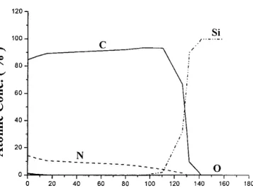
The depth profiles of C, N, O, and Si in nitrogen- doped amorphous diamond films were measured by AES analysis. As shown in Fig. 5 (data from 14.2 at.% nitrogen- doped film), a small number of oxygen atoms exit on the surface of film. In the AES spectrum, nitrogen distribu- tion in nitrogen-doped films and no oxygen atom in the film–substrate interface were observed. This suggests a
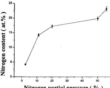
FIG. 2. Relationship between nitrogen partial pressure and nitrogen content in doped amorphous diamond films.
FIG. 3. Relative fraction of sp3-bonded C atom [sp3/(sp3+ sp2)] re- mains unchanged whatever the nitrogen content.
FIG. 1. (a) C 1s and (b) N1 s spectra of amorphous diamond films and curves fitted by Gaussian function.
uniform nitrogen distribution in nitrogen-doped films and no oxidation in the interface to increase barrier height of electron emission.
B. Measurement of Hall effect
The Hall effect was used to determine the electron concentration, mobility, and its resistivity. The depend- ence of these on nitrogen content of amorphous diamond films is revealed in Table I. The electron concentration of films increased with nitrogen content; however, mo- bility decreased with nitrogen content. The resistivity was found to decrease initially with nitrogen content and then it turned up by further increases of nitrogen; the lowest resistivity was achieved by 14.2 at.% nitrogen- doped film. From Table I and Fig. 3, decreasing resis- tivity is attributed to the Fermi level moving from near the valence band edge in the undoped amorphous dia- mond across the midgap and then to a position close to the conduction band mobility edge. Hence, it demon- strated that nitrogen acted as a true dopant in this study.
C. Electron field emission studies on amorphous diamond
Figure 6 shows AFM images of undoped and nitrogen- doped amorphous diamond films. The surface morphol- ogy of undoped and nitrogen-doped amorphous diamond films was very smooth (R
max⳱ 1.5 to 3.5 nm). Accord- ing to previous AFM studies, graphitization could dra- matically increase surface roughness.
17The measured AFM images before and after nitrogen addition clearly demonstrate that the addition of N
2does not change the morphology or roughness of the films. The AFM studies of films are in good agreement with ESCA (Fig. 3) and Raman results (Fig. 4), which also showed no graphiti- zation in nitrogen-doped films. It appeared that there was no local field enhancement due to surface irregularities;
for example, tips and protrusions. In this study, nitrogen enhancement dominated the electron emission from amorphous diamond.
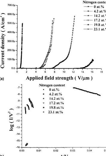
The field-emission-current density versus applied field strength (J–F ) curves of the amorphous diamond films with different nitrogen contents are shown in Fig. 7(a).
FIG. 4. (a) Typical Raman spectrum and (b) G peak positions of Raman spectra of nitrogen-doped amorphous diamond films.
FIG. 5. Depth profiles of nitrogen-doped amorphous diamond films by AES analysis.
TABLE I. The dependence of resistivity, electron concentration, and electron mobility on nitrogen content of amorphous diamond films.
Nitrogen content
(at.%)
Relative resistivity
(/o)
Relative electron concentration
(N/No)
Electron mobility (cm2/V × s)
0 1 1 158
4.2 1.02 1.08 146
14.2 0.89 1.22 145
17.2 0.96 1.29 126
19.8 1.27 1.67 74.5
23.1 3.07 1.87 30.3
o: resistivity of undoped amorphous diamond;: resistivity of nitrogen- doped amorphous diamond; No: electron concentration of undoped amor- phous diamond; N: electron concentration of nitrogen-doped amorphous diamond.
F–N plots (log (I/V
2) − 1/V curve) of amorphous dia- mond are shown in Fig. 7(b). From Fig. 7, the lowest
“turn-on” applied field strength was 0.7 V/m at the current density of 10 A/cm
2, and it was achieved by lowest resistivity nitrogen-doped film. Turn-on applied field strength, as a function of nitrogen content, de- creased up to certain nitrogen content and then increased at higher nitrogen content, as shown in Table II.
From Figs. 3, 4, 6, and 7 and Table I, it is demon- strated that nitrogen enhancement dominated the elec- tron emission from amorphous diamond due to raised Fermi level from near the valence band to near the con- duction band.
Another important practical characteristic for the elec- tron emission is the reproducibility of J–F plots with repeated increase/decrease of applied electric field.
20Sometimes field emitters showed hysteresis in emission properties, which is undesirable for practical applica- tions. However, the nature of hysteresis may shed light on the emission mechanism. To stabilize the emission property, all measurements were performed after a period
of “conditioning;” that is, the electric field was ramped up and down repeatedly until reproducible emission characteristics were observed. As demonstrated in Fig. 8, high reproducibility of field emission for nitrogen-doped amorphous diamond films deposited by cathodic arc was observed. There were no jumps in emission current nor hysteresis observed. The field-emission properties have been very consistent. This is in contrast to the high vari- ability observed for carbon nanotubes, as reported in the literature.
26,27TABLE II. Turn-on applied field strength of undoped and doped amorphous diamond films.
Nitrogen content (at.%)
Turn-on applied field strength (V/m) (turn-on current density: 10A/cm2)
0 5.4
4.2 14
14.2 0.7
17.2 4.95
19.8 7.78
23.1 Not turn on
FIG. 6. AFM images of (a) undoped and (b) doped amorphous dia- mond films.
FIG. 7. (a) Field-emission J–F curves and (b) F–N plots for the amor- phous diamond with different nitrogen contents.
IV. CONCLUSIONS
This research demonstrated how nitrogen doping af- fected field emission of amorphous diamond. ESCA, Raman, AFM, and Hall effect data clearly revealed that nitrogen doping raised the Fermi level of amorphous diamond from near the valence band to near the conduc- tion band. The narrowing down of band gap by the pres- ence of graphitic bonds (sp
2) was not observed. Turn-on applied field strength, as a function of nitrogen content, decreased up to a certain nitrogen content and then in- creased at higher nitrogen content. The lowest turn-on applied field strength was 0.7 V/ m at the current den- sity of 10 A/cm
2, and it was achieved by the lowest resistivity nitrogen-doped film. The field-emission characteristics of nitrogen-doped amorphous diamond films as deposited by cathodic arc were found highly reproducible.
ACKNOWLEDGMENTS
The authors would like to thank the National Science Council of Taiwan, Republic of China, for its financial support under Contract No. NSC91-2216-E-012-002. Ki- nik Company, Taiwan, Republic of China, provided all test samples. The Institute of Atomic and Molecular Sci- ences, Academia Sinica, Taipei, Taiwan, Republic of China, supported most of the characterization work.
REFERENCES
1. G.A.J. Amaratunga, M. Baxendale, N. Rupesinghe, I. Alexandrou, M. Chhowalla, T.B.A. Munindradasa, C.J. Kiley, L. Zhang, and T. Sakai, New Diamond and Frontier Carbon Technology 9, 31 (1999).
2. A.P. Burden, Int. Mater. Rev. 46, 213 (2001).
3. W.P. Kang, T. Fisher, and J.L. Davidson, New Diamond and Frontier Carbon Technology 11, 129 (2001).
4. V.G. Litovchenko, A.A. Evtukh, R.I. Marchenko, N.I. Klyui, and V.A. Semenovich, Appl. Surf. Sci. 111, 213 (1997).
5. A. Llie, A.C. Ferrari, T. Yangi, and J. Robertson, Appl. Phys. Lett.
76,2627 (2000).
6. K.H. Chen, J.J. Wu, L.C. Chen, C.Y. Wen, P.D. Kichambare, F.G. Tarntair, P.F. Kuo, S.W. Chang, and Y.F. Chen, Diamond Rel. Mater. 9, 1249 (2000).
7. W. Zhu, C. Bower, G.P. Kochanski, and S. Jin, Diamond Relat.
Mater. 10, 1709 (2001).
8. Y.H. Chen, C.T. Hu, and I.N. Lin, J. Appl. Phys. 84, 3890 (1998).
9. F.G. Tarntair, L.C. Chen, S.L. Wei, W.K. Hong, K.H. Chen, and H.C. Chen, J. Vac. Sci. Technol. B 18, 1207 (2000).
10. O. Gröning, O.M. Küttel, P. Gröning, and L. Schlapbach, Appl.
Surf. Sci. 111, 135 (1997).
11. S.E. Huq, P.D. Prewett, J.C. She, S.Z. Deng, and N.S. Xu, Mater.
Sci. Eng. B 74, 184 (2000).
12. W. Zhu, G.P. Kochanski, S. Jin, Science 282, 1471 (1998).
13. K. Okano, S. Koizumi, S.R.P. Silva, and G.A.J. Amaratunga, Nature 381, 140 (1996).
14. V.S. Veerasamy, J. Yuan, G.A.J. Amaratunga, W.I. Milne, K.W.R. Gilkes, M. Weiler, and L.M. Brown, Phys. Rev. B 48, 17954 (1993).
15. J. Robertson and C.A. Davis, Diamond Relat. Mater. 4, 441 (2001).
16. J.P. Xanthakis and A. Modinors, Diamond Relat. Mater. 9, 798 (1999).
17. Y.K. Hong, J.J. Kim, J.S. Kim, I.C. Jeon, C. Park, and J.K. Kim, Appl. Surf. Sci. 146, 269 (1999).
18. D. Hong and M. Aslam, J. Vac. Sci. Technol. B 12, 764 (1994).
19. F.Y. Wen, L.C. Chen, J.J. Wu, K.H. Chen, P.F. Kuo, C.W. Chang, Y.F. Chen, W.K. Hong, and H.C. Chen, Appl. Phys. Lett. 76, 2630 (2000).
20. V.V. Zhirnov, C.L. Rinne, G.J. Wojak, R.C. Sanwald, and J.J. Hren, J. Vac. Sci. Technol. B 19, 87 (2001).
21. B. Angleraud, N. Mubumbila, P.Y. Tessier, V. Fernandez, and G. Turban, Diamond Relat. Mater. 10, 1142 (2001).
22. S.T. Jackson and R.G. Nuzzo, Appl. Surf. Sci. 90, 195 (1995).
23. P. Petrov, D.B. Dimitrov, D. Papadimitrious, G. Beshkov, V. Krastev, and Ch. Georgiev, Appl. Surf. Sci. 151, 233 (1999).
24. E. Liu, X. Shi, B.K. Tay, L.K. Cheah, H.S. Tan, J.R. Shi, and Z. Sun, J. Appl. Phys. 86, 6078 (1999).
25. M. Chhowalla, A.C. Ferrari, J. Robertson, and G.A.J. Amaratunga, Appl. Phys. Lett. 76, 1419 (2000).
26. K.A. Dean and B.R. Chalamala, Appl. Phys. Lett. 76, 375 (2000).
27. S.H. Lim, H.S. Kim, C.H. Lee, S.T. Pietruszko, and J. Jang, J. Non-Cryst. Solids 299–302, 864 (2002).
FIG. 8. The reproducibility of field emission for doped amorphous diamond film.