for GHz RF Transmitter Applications
Chung-Yu Wu, Fellow, IEEE, and Hong-Sing Kao, Student Member, IEEE
Abstract—A compact low-voltage low-power CMOS di-rect-conversion quadrature modulator with integrated quadra-ture voltage-controlled oscillator (VCO) and radio frequency (RF) amplifier for wireless transmitter applications is proposed and analyzed. By applying both baseband input signals with quadrature phases and quadrature local oscillator (LO) signals to a set of combiners, the quadrature modulation functions can be implemented. The low-power operation is enabled by the current reuse technique used among quadrature modulator, quadrature VCO, and RF amplifier. Because only two transistors and one re-sistor are cascoded in the critical path of the proposed quadrature modulator between power supply and ground, the supply voltage can be as low as 1.5 V. The proposed circuit structure is used to design a quadrature modulator chip for 1.9-GHz digital enhanced cordless telecommunications (DECT) transmitter applications. The experimental chip is fabricated by using 0.35- m n-well double-poly-triple-metal (DPTM) CMOS technology. The power dissipation is only 18 mW under 2-V power supply voltage. The on-chip quadrature VCO can provide highly accurate quadrature signals without any phase tuning or trimming. The frequency tuning range of the quadrature VCO is 280 MHz from 1.89 to 2.17 GHz at 2-V supply voltage. Due to small mismatch among quadrature signal paths, the measured image ratio is below 42 dBc under 2-V supply voltage when the desired upper side-band (USB) is set at 2 GHz and 51 dBc under 3-V supply voltage when the desired USB at 1.94 GHz. At 2-V supply voltage, the measured LO leakage is 48 dBc. Moreover, the measured second-order intermodulation and third-order intermodulation are less than
46 dBc.
Index Terms—CMOS technology, current reuse, direct-conver-sion, low-power, low-voltage, quadrature modulator, quadrature voltage-controlled oscillator (VCO), radio frequency (RF), RF am-plifier, transmitter, wireless communication.
I. INTRODUCTION
I
N RADIO frequency (RF) transmitters operated in the gigahertz range, the quadrature modulator is one of the key components, which has significant effects on the quality of modulated signals. Generally, direct-conversion [1] and hetero-dyne [2] are the two major methods for quadrature modulation.Manuscript received October 28, 2000; revised January 17, 2002. This work was supported by the National Science Council (NSC), Taiwan, R.O.C., under Grant NSC89-2215-E-009-064. This paper was recommended by Associate Ed-itor K. Mannetakis.
The authors are with the Integrated Circuits and Systems Laboratory, Institute of Electronics, National Chiao Tung University, Hsinchu, Taiwan 300, R.O.C. (e-mail: [email protected]).
Publisher Item Identifier S 1057-7130(02)04747-X.
Fig. 1. Block diagram of the RF transmitter including direct-conversion quadrature modulator core, quadrature VCO, RF amplifier, and power amplifier.
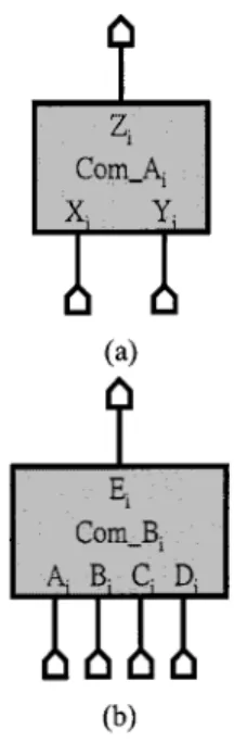
Fig. 2. (a) Block diagram of type-A 2-input combiner. (b) Block diagram of type-B 4-input combiner.
Fig. 1 shows the block diagram of a RF transmitter system which consists of the direct-conversion quadrature modulator core, quadrature voltage-controlled oscillator (VCO), RF am-plifier, and power amplifier. The direct-conversion quadrature modulator core formed by two mixers and one adder, converts the baseband signals and the local oscillator (LO)
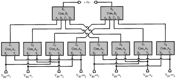
Fig. 3. Block diagram of the direct-conversion quadrature modulator core structure.
signals into the single-side-band output signal. This compact structure can effectively reduce cost, power dissipation, and chip area as compared to the heterodyne quadrature modulator. In addition, both bandwidth and data rate can be improved.
In modern RF mobile transceiver systems, small form factor, lightweight, low cost, and low power dissipation are indispens-able. To implement these systems, integrated circuits (ICs) with high integration level and low power dissipation are required. It is known that the submicron CMOS technology has great poten-tial for RF transceiver design with medium output power. Gener-ally, RF CMOS communication ICs have the advantages of low voltage, low power, low cost, and high integration. So far, many RF CMOS quadrature modulator designs have been reported [1]–[7]. Among them, an 1.9 GHz low-distortion direct-con-version quadrature modulator realized by 0.5- m CMOS tech-nology, has been proposed by the present authors [6] where a new mixer circuit is designed to achieve low power dissipation at 3-V supply voltage. It has been shown that the realized di-rect-conversion quadrature modulator has good performance in image rejection and LO leakage [6].
In the quadrature modulator, highly accurate quadrature signals from the LO are required. So far, there have been four methods proposed to generate LO signals with quadra-ture phases [8]–[16]. They are: 1) Resistance–capacitance capacitance–resistance (RC–CR) phase shifter [8] and [9]; 2) frequency divider [10]; 3) even-stage ring oscillator [11]–[14]; and 4) two direct-coupled and cross-coupled inductance–ca-pacitance ( )-load VCOs [15] and [16]. Among them, the -load VCO has low phase noise and stable oscillation frequency.
In this paper, an improved CMOS direct-conversion quadra-ture modulator with integrated RF amplifier and -load quadrature VCO, as indicated by the shaded area in Fig. 1, for low-voltage and low-power RF transmitter applications is proposed and analyzed [17]. In the proposed quadrature modulator, two types of combiners [6] and [18] are connected to form the quadrature modulator core [6] which performs the low-distortion direct-conversion quadrature modulation func-tion. The circuits of input and output combiners are modified to allow the combination with quadrature VCO and RF amplifier,
respectively. The quadrature VCO merged to the input com-biner is based on the two-stage ring oscillator with tanks as output loads. It has low phase error and low phase noise. The circuit of RF amplifier is also merged to the output combiner in the proposed quadrature modulator. Thus, the output combiner has voltage gain only within the desired band. In the proposed highly integrated new direct-conversion quadrature modulator, the power dissipation can be reduced to 18 mW at 2 V. LO leakage is low and image rejection is high. It is shown from experimental results that the proposed modulator operated at 1.9 GHz can satisfy the specifications of the RF transmitter in digital enhanced cordless telecommunications (DECT) systems [19]. It is expected that the proposed modulators can also be applied to other wireless communication systems like Bluetooth [20] or wireless LAN [21].
In Section II, the operational principles of direct-conversion quadrature modulator core, -load ring-oscillator quadrature VCO, and the overall modulator structure are described. In Sec-tion III, the circuit structure of the proposed quadrature modu-lator with quadrature VCO merged to type-A combiner and RF amplifier to type-B combiner is analyzed. In Section IV, experi-mental results of the proposed CMOS quadrature modulator are described. Finally, the conclusion is given in Section V.
II. OPERATIONALPRINCIPLE
In the proposed quadrature modulator, two types of com-biners are used [6] and [18] to form the modulator core cir-cuit. One is the type-A two-input combiner and the other is the type-B four-input combiner. Their block diagrams are shown in Fig. 2(a) and (b), respectively. The output signals and of these two combiners can be expressed as [6] and [18]
Type A (1)
Type B (2) In (1), is the output of the two-input combiner Com
, and are the inputs to Com , and are constants. In (2), is the output of the four-input combiner
Fig. 4. Cascoded architecture which enables the current reuse technique among quadrature VCO, combiners, and RF amplifier.
Com , , , , and are the inputs to Com , and are constants.
The structure of the direct-conversion quadrature modulator core is shown in Fig. 3 where the input signals are applied to eight type-A combiners (Com Com ) and the output is taken as the difference of the outputs of two type-B combiners (Com and Com ). Assume that the common-mode dc voltage is imposed upon the input signals and whereas the common-mode dc voltage upon the input sig-nals and . Then the inputs to and , and , and , and and can be written as , , , and whereas those to and , and , and , and and as , ,
, and , respectively. Note that and ( and ) are quadrature signals. Substituting the input voltages of and into (1), the outputs ( ) of Com Com (Com Com ) can be expressed in the form of (1) with the input signals and ( and ).
Since , , , and ( , , , and ) are sent to the inputs of the combiners Com (Com ), its output ( ) can be obtained from (2) with ( ), ( ), ( ), and ( ). The output signal
can be derived by substituting as functions of , , , and into (2). Through some calculations, it can be found that if and , the undesired terms in the expression of can be canceled and the resultant is
(3) This verifies the quadrature modulation function of the direct-conversion quadrature modulator core in Fig. 3. It can be seen from (3) that both second-order terms and of the input combiner and first-order terms of the output com-biners have no effects on the quadrature modulator function.
In order to efficiently reduce chip area, power dissipation, and quadrature phase error, the quadrature VCO is cascoded with eight type-A combiners whereas RF amplifier is merged to two type-B combiners as shown in the block diagram of Fig. 4. As may be seen from Fig. 4, the cascoded quadrature VCO and type-A combiners uses the same current (5.8 mA) whereas the combined type-B combiner and RF amplifier uses the same (3.2 mA). In this way, the total power dissipation can be re-duced approximately to one half of the original one. Further-more, the signal paths from quadrature VCO to quadrature mod-ulator can be kept very short and symmetrical to alleviate the
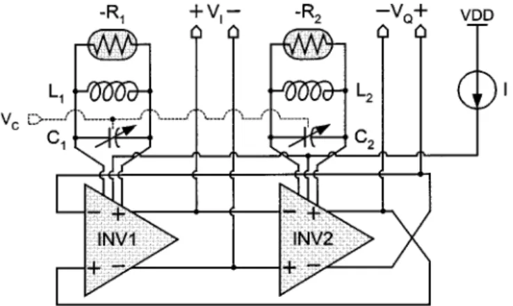
in-Fig. 5. Conceptual block diagram of the quadrature VCO.
Fig. 6. (a) Circuit diagram of type-A 2-input combiners. (b) Circuit diagram of type-B 4-input combiners.
fluence on the quadrature phases of VCO output signals by the parasitic components on the signal paths. Thus, the phase error can be minimized.
To implement the integrated quadrature VCO in Fig. 4, a new circuit structure based on the even-stage ring oscillator is pro-posed [22]. Fig. 5 shows the conceptual block diagram of the proposed quadrature VCO where two fully differential inverters with on-chip -tank loads and negative resistors are connected to form a two-stage ring oscillator. Only two inverter stages with two spiral inductors are used so that both chip area and power dissipation can be saved. Moreover, the current of the two in-verters is kept constant by the current source [22] as shown in Fig. 5. This can reduce power dissipation [16] and enhance the phase accuracy of the quadrature signals [22].
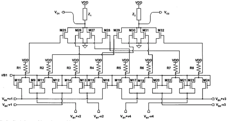
Fig. 7. Circuit diagram of the quadrature modulator.
In Fig. 5, tanks are used as inverter loads in the two-stage ring oscillator. Thus, the phase noise can be reduced. The two tanks are realized by on-chip spiral inductors ( ) and variable capacitors ( ). The negative resistors (
) connected in parallel with the tanks, are required to cancel the series resistance effect of spiral inductors and guar-antee oscillation. The two variable capacitors can be tuned si-multaneously by the control voltage from the frequency syn-thesizer to obtain the desired oscillation frequency expressed as Hz which is independent of the bias current of the inverters. The maximum impedance of the -load occurs at the oscillation frequency. At this frequency, the fully differen-tial inverter achieves the maximum gain and the ring oscillator can maintain the quadrature oscillation. At other frequencies, the impedance of the -load decreases and the gain of the fully differential inverter also decreases. Thus, the ring oscil-lator cannot maintain the quadrature oscillation.
At oscillation, the delay times of the two fully differential inverters of Fig. 5 are always kept the same so that their outputs can provide highly accurate quadrature signals. To achieve equal delay times in these two fully differential inverters, symmetrical layout topologies must be used.
III. CIRCUITDESIGN A. Quadrature Modulator
Since the long-channel MOS transistor is basically a square-law device, the second-order transfer function in (1) can be implemented by long-channel MOS transistors [18]. Fig. 6(a) shows the type-A combiner circuit where the drain terminals of the MOS transistors M1 and M2 are connected to the resistor . In the type-A combiner of Fig. 6(a), two inputs are applied to the sources of MOS transistors with their gates biased at . This arrangement allows both quadrature
VCO and baseband circuits be cascoded with the combiners to achieve the current reuse. Thus, power dissipation can be reduced.
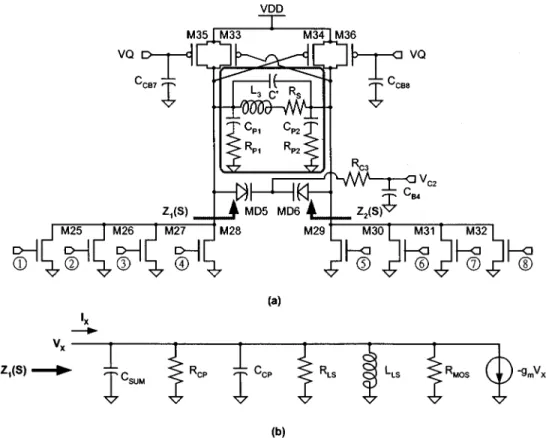
The circuit of the type-B combiner is shown in Fig. 6(b) where the drain terminals of the MOS transistors M1, M2, M3, and M4 are connected to the impedance and their input gate signals are denoted as , , , and , respectively. Since the RF amplifier is merged to the type-B combiner, the resistor load is changed to the -tank load to obtain the narrow-band characteristics at the output node.
The transfer characteristics of the two combiners in Fig. 6 can be modeled by the drain current equation of long-channel MOS transistors in the saturation region. Using the ideal square-law current identity of long-channel MOS transistors, the drain cur-rent can be expressed as
(4) where is the transconductance param-eter, is the effective surface carrier mobility, is gate oxide capacitance per unit area, ( ) is the channel width (length) of the MOS device, is the gate–source voltage, and is the threshold voltage. Because the source voltage of the MOS device in the type-A combiner is not the same as its sub-strate voltage, the body effect exists and the threshold voltage is dependent on the source-substrate voltage . Its expression is (5) where is the threshold voltage with zero , is called the body-effect constant, and is the surface potential under strong inversion.
If M1 and M2 in the type-A combiner are operated in the saturation region, the output voltage at the drain terminal
Fig. 8. LC-tuned fully differential inverter.
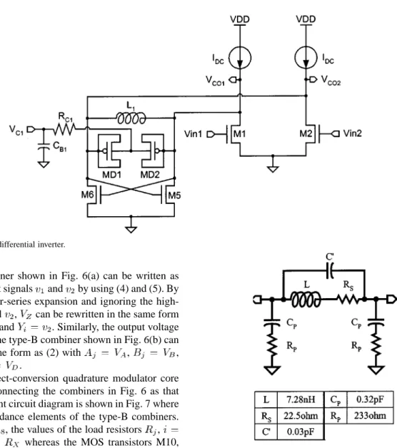
of the type-A combiner shown in Fig. 6(a) can be written as functions of the input signals and by using (4) and (5). By employing the Taylor-series expansion and ignoring the high-order terms of and , can be rewritten in the same form as (1) with and . Similarly, the output voltage at the output of the type-B combiner shown in Fig. 6(b) can be written in the same form as (2) with , ,
, and .
The complete direct-conversion quadrature modulator core can be formed by connecting the combiners in Fig. 6 as that in Fig. 3. The resultant circuit diagram is shown in Fig. 7 where and are impedance elements of the type-B combiners. In Com Com , the values of the load resistors ,
, are denoted as whereas the MOS transistors M10, M12, M14, M16, M18, M20, M22, and M24 (M9, M11, M13, M15, M17, M19, M21, and M23) are identical with the same ( ). From the derived equation, one can obtain the corresponding coefficients and as
(6)
where ,
, ,
, and .
In Com and Com , the values of and are de-noted by whereas all the MOS transistors M25 M32 are identical with the same . The body effect does not appear in the type-B combiner, because both sources and substrates of MOS transistors M25 M32 are all connected to ground. There-fore, their threshold voltages are identical and denoted as . Using , , and in the derived equation, one can obtain the corresponding coefficient as
(7)
Fig. 9. Equivalent circuit of the spiral inductor.
The output voltage can be derived by substituting and in (6) and in (7) into (3). The result is
(8) As seen in (8), the function of the direct-conversion quadra-ture modulator core is realized. The body effect in the type-A combiners leads to the slight reduction of the gain of quadrature modulator core. But this gain reduction can be compensated by the gain enhancement of the type-B combiner with the -tank load.
The above derivation of the quadrature modulation function is based on the assumptions of square-law MOS characteris-tics and completely matched devices or components. However, some nonideal effects exist to affect the quadrature modulation function. Besides the body effect, the major nonideal effects are mobility degradation effect, channel-length modulation effect, and velocity saturation effect of MOS devices as well as device or component mismatches due to process variations. It is shown
Fig. 10. (a) Circuit diagram of the RF amplifier merged to the type-B combiners. (b) Equivalent half circuit of the load impedance.
that most high-order harmonic terms at the output of the pro-posed quadrature modulator core caused by mobility degrada-tion and channel-length moduladegrada-tion effects can be canceled due to the fully balanced structure [18]. Thus, these nonideal effects only have little contribution to the intermodulation error of the quadrature modulator core.
In short-channel MOS devices, the velocity saturation effect makes the drain current proportional to where . In the saturation region where the velocity satura-tion effect dominates, we have . If short-channel MOS devices operated in this region with are used, the type-A combiners still can function properly with in (3) as mentioned in Section II. But the type-B combiners cannot function properly since in (3). In the modulator core design for transmitter applications, short-channel MOS devices are used in both type-A and type-B combiners to obtain high frequency response in the gigahertz range. In the type-B com-biners, the gate voltage of the MOS devices should be kept low enough to avoid . In our design, the MOS devices of type-B combiners have the drawn channel length of 0.35 m and the drawn channel width of 20 m. The dc gate bias voltage is kept between 0.7 and 0.9 V with the corresponding between 150 and 550 A. In this region, and the linearity error is below 4.3% for 300-mV peak-to-peak amplitude of input sig-nals. This is acceptable in this modulator core design.
Another important error source of the proposed quadrature modulator core is the device or component mismatch which de-grades the performance of image rejection and intermodulation. This is because the quadrature modulation function in (8) is real-ized by canceling the undesired terms at the output, which relies on the matched characteristics of devices or components. In the
direct-conversion quadrature modulator core of Fig. 7, the MOS device parameters to be matched are the transconductances , , and as well as the threshold voltages , , and . The passive components to be matched are the resistors and the impedances and . When the per-fect match is assumed in the HSPICE simulation of the proposed quadrature modulator operated at 2 V, the simulated image ratio, LO leakage, second-order intermodulation, and third-order in-termodulation are less than 80 dBc. But when 1% 5% MOS device mismatch is applied to the two MOS devices M18 and M24 of the type-A combiners in the baseband- path, the sim-ulated image ratio, LO leakage, second-order intermodulation, and third-order intermodulation are degraded by 5.5, 5.6, 4, and 6 dBc per 1% mismatch, respectively. This mismatch represents the worst-case one where both local mismatch within the type-A combiner between the baseband- and LO- signals and global mismatch between the type-A combiners for and signals exist. Similarly, when 1% 5% MOS device mismatch is ap-plied to the two type-B combiners in the output stage, the sim-ulated image ratio, LO leakage, second-order intermodulation, and third-order intermodulation are degraded by 7, 3.5, 14, and 10 dBc per 1% mismatch, respectively.
Generally, good matching characteristics can be obtained by special layout methods. In order to minimize the device mis-match due to process variations, the MOS devices of the type-A combiners in the baseband- (LO- ) path are interlaced with those in the baseband- (LO- ) path. The two type-B com-biners are placed as close as possible. Some dummy resistors are placed around the edge of the resistor array to make the same environment for the active resistors. Moreover, the paths from the outputs of the type-A combiners to the inputs of the type-B
Fig. 11. Complete circuit diagram of the direct-conversion quadrature modulator with integrated quadrature VCO and RF amplifier.
combiners must be kept symmetrical to achieve equal parasitic components. Some ground planes and lines are used to avoid the signal cross-talk.
B. Merged Quadrature VCO
Fig. 8 shows the circuit diagram of the -tuned fully differ-ential inverter used in the quadrature VCO. In Fig. 8, the MOS transistors M1 and M2 form the differential amplifier that con-verts input differential voltage into output differential current. The negative resistor in Fig. 5 is realized by two cross-coupled MOS transistors M5 and M6 to provide enough negative resis-tance for oscillation. The variable capacitor in Fig. 5 is imple-mented by two p /n-well junction varactors MD1 and MD2 as shown in Fig. 8. The cathodes of the two junction varactors are connected through the series resistor and the shunt capacitor to the control voltage from the frequency synthesizer. Through , the dc bias voltages of the two junctions can be adjusted to change the value of junction capacitance and, thus, the VCO frequency.
To merge the quadrature VCO with the input combiners of the quadrature modulator core, the structure of the -tuned inverter is modified by folding both -tank load and negative resistor down to ground as shown in Fig. 8. Then the drain nodes of M1 and M2 can be connected to the source nodes of the MOS devices in the type-A combiners. Since the combiners provide
the constant bias currents to the differential inverter via the drain nodes of M1 and M2, two dc current sources denoted by are added to the inverter of Fig. 8.
The on-chip spiral inductor is characterized by the -type equivalent circuit shown in Fig. 9 where the component values can be determined from measurement as nH,
, pF, , and PF [23]. In the equivalent circuit of Fig. 9, is the inductance of the spiral inductor, is the parasitic series resistance of spiral inductor, is the silicon substrate resistance, is the oxide capacitance between spiral inductor and substrate, and is the overlap capacitance between spiral inductor and the center-tap underpass.
C. Merged RF Amplifier
To save the power dissipation, the RF amplifier [6] is merged to the type-B combiners as shown in Fig. 4. The merged circuit is shown in Fig. 10(a) where the impedance elements and in Fig. 7 are implemented by the on-chip spiral inductor in parallel with the p /n-well junction varactors MD5 and MD6. The spiral inductor in the merged RF amplifier is the same as that in the merged quadrature VCO. MD5 and MD6 are the tunable junction varactors controlled by through the resistor and the bypass capacitor for center-frequency tuning. Although MD5 and MD6 are made tunable in this experimental
chip design, fixed capacitors can be used to avoid the tuning process. M33 and M34 in Fig. 10(a) are cross-coupled to realize the negative resistance in parallel with the tank to cancel the series resistance of the spiral inductor. The negative resistance can be adjusted by the gate voltage of the MOS transistors M35 and M36 so that the tuning can be achieved. Practically, the negative resistance can be fixed without tuning. There are two advantages for using only one tank as the load of the two type-B combiners. First, only one spiral inductor is used so that the chip area is reduced. Second, the MOS transistors M33 M36 which realize the adjustable negative resistance, are cascoded to the input devices of type-B combiner so that the current is reused to save power dissipation.
Because of the symmetrical structures of the merged RF am-plifier circuit in the differential branches, the equivalent half circuit of the load impedance or is shown in Fig. 10(b) which can be used to derive the transfer function of the type-B combiner. For simplicity, the series connection of components is transformed into the equivalent parallel connection. The com-ponent values of the equivalent half circuit can be derived as
(9) where is the frequency of the modulated signal at output nodes, , , and are the drain-sub-strate capacitances of the MOS transistors M25 M28, M33, and M35, respectively, , , and are the gate–drain capacitances of MOS transistors M33, M34, and M35, respectively, is the equivalent capacitance of junc-tion varactors MD5 and MD6, is the input capacitance load of the output buffer including the parasitic capacitance of the metal connection lines, , , and are the output resistances of MOS transistors M25 M28, M33, and M35, respectively, and is the current bias in the MOS transistor M33.
The admittance at the output node of the type-B com-biners with the merged RF amplifiers can be express as
(10)
TABLE I
DEVICEDIMENSIONS ANDCOMPONENTVALUES OF THEQUADRATURE
MODULATORWITHINTEGRATEDQUADRATUREVCOANDRF AMPLIFIER
To prevent the poles from running into the right half plane and causing instability, the real part of must be kept positive by choosing as
D. Overall Circuit
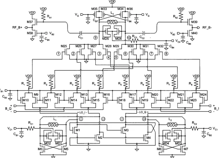
The complete circuit of the proposed quadrature modulator is shown in Fig. 11. As may be seen from Fig. 11, the base-band differential signals and are applied to the quadrature modulator core from the sources of M18, M20, M22, M24 and M10, M12, M14, M16 whereas the LO signals LO- and LO- from the sources of M9, M11, M13, M15 and M17, M19, M21, M23, respectively. Thus, the upper-side-band (USB) signal can be obtained at the output. The baseband cir-cuit may also be merged to the quadrature modulator core as the quadrature VCO. Alternatively, constant current sources can be connected to the sources of these MOS devices to maintain the dc voltage and current while the signals are input to the sources through dc blocking capacitors.
For the measurement on the output differential signals of the merged RF amplifier, its differential output nodes and are connected to the output buffers through the dc blocking ca-pacitors and as shown in Fig. 11. The output buffers are simple NMOS source followers M37, M38, M39, and M40. Their outputs RF_B and RF_B are connected directly to bonding pads for signal measurement. In the source followers, the current sources are realized by M38 and M40 biased at whereas the gates of driving NMOS transistors M37 and M39 are biased at through the resistors. Since the output signal amplitude is kept smaller than , M37 and M39 can be kept in the saturation region.
Fig. 12. Microphotograph of the fabricated direct-conversion quadrature modulator chip.
Fig. 13. External baseband input circuit in the measurement set-up to provide constant current and baseband differential signals B Q for the quadrature modulator.
The bias currents of the quadrature VCO merged with type-A combiner and RF amplifier merged with type-B combiner are 5.8 mA and 3.2 mA, respectively. The component values and channel dimensions of MOS devices of Fig. 11 are summarized in Table I.
IV. EXPERIMENTALRESULTS
The proposed low-voltage and low-power direct-conversion quadrature modulator structure in Fig. 11 is used to design an 1.9 GHz version for the DECT system. The experimental chip is fabricated by using 0.35- m double-poly triple-metal (DPTM) CMOS technology. All the resistors in Fig. 11 are implemented by n ploysilicon to provide stable resistance with low tem-perature coefficient, whereas all the linear capacitors are im-plemented by using the polysilicon-to-polysilicon capacitor for good reliability. The microphotograph of the experimental chip
Fig. 14. Measurement set-up.
Fig. 15. Photograph of the circuit test fixture.
is show in Fig. 12. The active area is 900 m 1200 m, dom-inated by the three large on-chip spiral inductors.
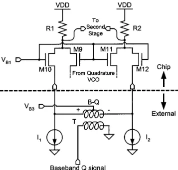
In the measurement set-up, the four baseband inputs are bi-ased by current sources formed by external discrete devices. Fig. 13 shows the external baseband input circuit for and the same circuit is also used for . As shown in Fig. 13, the baseband differential signal is generated from a RF transformer with the secondary center tap connected to a fixed bias . This transformer performs the single-ended-input-to-differential-output conversion to generate the differential signal . The bias is carefully chosen so that the current of the input MOS with is equal to that of the external current source. This guarantees no dc current flowing through the transformer .
Fig. 14 shows the overall measurement set-up of the fabri-cated quadrature modulator chip. The baseband signals are generated by an arbitrarily waveform generator whereas the output signal is measured by a spectrum analyzer. The 10-MHz 300-mV single-ended baseband inputs are converted into differential signals by using the RF transformers and then ap-plied to the fabricated quadrature modulator chip. The RF mod-ulated signal is measured through a RF output balun. The fab-ricated chip is measured under the nominal 2 V power supply voltage. Fig. 15 shows the photograph of the circuit test fixture
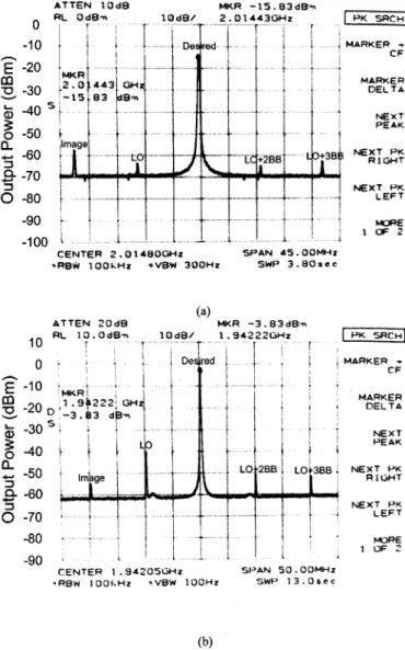
Fig. 16. Measured output spectrums of the fabricated direct-conversion quadrature modulator chip with (a) 2 V and (b) 3 V supply voltages.
with the fabricated chip directly mounted on the PCB. In order to reduce the parasitic inductance of bonding wires, the substrate of PCB under the chip is dug down to make the surfaces of both PCB and chip on the same plane.
Fig. 16(a) shows the measured output spectrum of the fabricated direct-conversion quadrature modulator chip under 2-V power supply voltage, where the desired output is the upper side-band (USB) component and the image output is the lower side-band (LSB) component. The measured output power of the modulated signal is 15 dBm when the baseband signal of 10 MHz 300 mV is applied and the voltage of the merged RF amplifier is set to 2 V. The LO leakage is 48 dBc referred to 15 dBm output power whereas the measured image ratio is 42 dBc. The second-order intermodulation (LO 2 BB) components are less than 49 dBc referred to 15 dBm desired output power, whereas the third-order inter-modulation (LO 3 BB) components are less than 47 dBc. Since the current reuse technique is used, the total current drain in the quadrature modulator with integrated quadrature VCO and RF amplifier is only 9 mA under 2-V power supply voltage.
Fig. 17. Measured tuning characteristic of the quadrature VCO.
Fig. 18. Measured output phase noise of the quadrature VCO.
Fig. 16(b) shows the measured output spectrum of the quadra-ture modulator under 3 V power supply voltage. The measured output power of modulated signal is 4 dBm when the base-band signal of 10 MHz 300 mV is applied. The image ratio, LO leakage, LO 2 BB, and LO 3 BB referred to 4 dBm output power are 51, 36, 47, and 46 dBc, respectively.
The measured image ratio of the fabricated quadrature modulator under 2-V supply voltage is degraded to 42 dBc as compared 51 dBc under 3-V. This degradation is due to the inherent device mismatches of the combiners which become more significant as supply voltage is smaller.
It is noted that the measured output power is 4.7 dBm smaller than the post-simulation result. This is because the values of fabricated polysilicon resistors are larger than the designed values. Due to the larger voltage drop on the resistors, the dc voltages at the nodes in Fig. 11 is decreased, which leads to the decrease of of M25 M32 and the decrease of the gain of type-B combiners. Thus, the quadrature modulator cannot provide the desired output level. The effect of resistor variations can be reduced by using dc blocking capacitors between type-A and type-B combiners or making the bias voltage of the type-A combiners tracking with the variations of .
Fig. 17 shows the tuning characteristic of the quadrature VCO under different supply voltages. It can be seen from Fig. 17 that the tuning range of 280 MHz is achieved in the
Fig. 19. Dependence of output power on power supply voltage at RF signal frequency of 2 GHz and 10 MHz basebandI=Q signals amplitude of 300 mV .
Fig. 20. Measured frequency dependence of output power, LO leakage, and image ratio of the fabricated quadrature modulator chip under 2 V power supply voltage.
quadrature VCO when the control voltage is changed from 0 to 2 V under 2-V supply voltage and 310 MHz when the control voltage is changed from 0 to 3 V under 3 V supply voltage. The tuning range is larger than the frequency band of 20 MHz (1.88 GH 1.9 GHz) in the DECT system. The center frequency is around 2.05 GHz which is higher than the DECT specification of 1.89 GHz. But this difference can be easily corrected by increasing the values of the varactors in the quadrature VCO. Since the tuning characteristic of the quadrature VCO is quite linear, it is useful for many applications.
The simulated output amplitude of the quadrature VCO is 0.12 V. Fig. 18 shows the measured output phase noise of the quadrature VCO which is implemented on a separated chip for measurement purpose. With the quality factor of the on-chip spiral inductor being 1.74, the measured phase noise of the quadrature VCO at 100-kHz and 1-MHz offset are 94.33 and 112.33 dBc/Hz, respectively. It does not contribute to unallowable emissions near the band edge of the DECT standard.
The dependence of output power on power supply voltage is shown in Fig. 19 where the output power is increased with the supply voltage. As may be seen from Fig. 19, the supply voltage can be as low as 1.5 V. This is because there are only two transistors and one resistor connected from power supply to ground in the critical path of the quadrature modulator and the threshold voltage of the transistor is as low as 0.58 V 0.69 V in this technology.
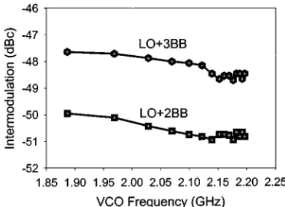
Fig. 21. Measured frequency dependence of intermodulation on VCO frequency for the fabricated quadrature modulator under 2 V power supply voltage.
TABLE II
MEASUREDPERFORMANCE OF THEFABRICATEDQUADRATUREMODULATOR
CHIPWITHINTEGRATEDQUADRATUREVCOANDRF AMPLIFIER
Fig. 20 shows the measured frequency dependence of output power, LO leakage, and image ratio of the fabricated quadrature modulator chip under 2-V supply voltage. Between 1.89 and 2.2 GHz, the output power is larger than 16 dBm, the LO leakage is less than 47 dBc, and the image ratio is less than 40 dBc. Fig. 21 shows the measured frequency dependence of the intermodulation for the fabricated quadrature modulator chip under 2 V supply voltage. Since the quality factor of the load of the type-B combiner at higher frequency is larger than that at lower frequency, the selectivity is better at higher frequency. This leads to smaller image ratio, LO leakage, and intermodulation at higher frequency as shown in Figs. 20 and 21.
All the measured results of the fabricated quadrature modu-lator chip with integrated quadrature VCO and RF amplifier are summarized in Table II.
V. CONCLUSION
A compact 2 V low-power direct-conversion quadrature modulator with integrated quadrature VCO and RF amplifier has been proposed. In the proposed quadrature modulator, both quadrature VCO and RF amplifier are merged to the quadrature
modulator core by using the current reuse technique. Thus, power dissipation can be reduced significantly. Due to the symmetrical and merged structure of the modulator, the mis-matches among quadrature signal paths can be minimized to increase the image rejection. The proposed circuit structure has been adopted to design the quadrature modulator chip for 1.9 -GHz DECT transmitter application. The chip is fabricated by using 0.35- m DPTM CMOS technology. The measured image ratio of 42 and 51 dBc can be achieved with 2 and 3 -V supply voltages, respectively. Under 2-V supply voltage, the measured LO leakage is 48 dBc whereas the measured second-order intermodulation, third-order intermodulation, and other spurious components are less than 47 dBc. The tuning range is 280 MHz in the quadrature VCO. Through extensive measurement, the performance of the proposed low-power quadrature modulator for DECT transmitter application has been verified. It is also suitable for other RF transmitter applications.
ACKNOWLEDGMENT
The authors would like to thank the Chip Implementation Center (CIC) of National Science Council (NSC) of Taiwan, R.O.C. for their support in chip fabrication.
REFERENCES
[1] M. Borremans, M. Steyaert, and T. Yoshitomi, “A 1.5V, wide band 3GHz, CMOS quadrature direct up-converter for multi-mode wireless communications,” in Proc. IEEE Custom IC Conf., 1998, pp. 79–82. [2] C. Marshall, F. Behbahani, W. Birth, A. Fotowat, T. Fuchs, R. Gaethke,
E. Heimerl, S. Lee, P. Moore, S. Navid, and E. Saur, “A 2.7V GSM transceiver IC’s with on-chip filtering,” in Proc. ISSCC Dig. Tech.
Pa-pers, Feb. 1995, pp. 148–149.
[3] T. P. Liu, E. Westerwick, N. Rohani, and R. H. Yan, “5GHz CMOS radio transceiver front-end chipset,” in Proc. ISSCC Dig. Tech. Papers, Feb. 2000, pp. 320–321.
[4] S. Sheng, L. Lynn, J. Peroulas, K. Stone, I. O’Donnell, and R. Brodersen, “A low-power CMOS chipset for spread-spectrum communications,” in
Proc. ISSCC Dig. Tech. Papers, Feb. 1996, pp. 346–347.
[5] M. Steyaert, M. Borremans, J. Janssens, B. D. Muer, N. Itoh, J. Craninckx, J. Crols, E. Morifuji, H. S. Momose, and W. Sansen, “A single-chip CMOS transceiver for DCS-1800 wireless communica-tions,” in Proc. ISSCC Dig. Tech. Papers, Feb. 1998, pp. 48–49. [6] C.-Y. Wu and H.-S. Kao, “A 3V 1.9GHz CMOS low-distortion
direct-conversion quadrature modulator with an RF amplifier,” in Proc. Int.
Conf. Electronics, Circuits, and Systems, vol. 2, Sept. 1999, pp. 777–780.
[7] B. Razavi, “A 900-MHz/1.8-GHz CMOS transmitter for dual-band ap-plications,” IEEE J. Solid-State Circuits, vol. 34, pp. 573–579, May 1999.
[8] J. Sevenhans, A. Vanwelsenaers, J. Wenin, and J. Baro, “An integrated Si bipolar RF transceiver for a zero IF 900MHz GSM digital mobile radio front-end of a hand portable phone,” in Proc. IEEE Custom IC Conf., 1991, pp. 7.7.1–7.7.4.
[9] I. A. Koullias, S. L. Forgues, and P. C. Davis, “A 100 MHz IF am-plifier/quadrature demodulator for GSM cellular radio mobile termi-nals,” in Proc. IEEE Bipolar Circuits and Technology Meeting, 1990, pp. 248–249.
[10] J. Fenk, W. Birth, R. G. Irvine, P. Sehrig, and K. R. Schon, “An RF front-end for digital mobile radio,” in Bipolar Circ. and Tech. Mtg., Min-neapolis, MN, 1990, pp. 244–247.
[11] J. McNeill and R. Croughwell, “A 150mW, 155MHz phase-locked-loop with low jitter VCO,” in Proc. IEEE Int. Symp. Circuits and Systems, vol. 3, June 1994, pp. 49–52.
[12] A. W. Buchwald and K. W. Martin, “High-speed voltage-controlled os-cillator with quadrature outputs,” Electron. Lett., vol. 27, pp. 309–310, 1991.
[13] Y. Sugimoto and T. Ueno, “The design of a 1-V, 1-GHz CMOS VCO circuit with in-phase and quadrature-phase outputs,” in Proc. IEEE Int.
Symp. Circuits and Systems, Hong Kong, June 1997, pp. 269–272.
[14] J. Tang and D. Kasperkovitz, “A 0.9–2.2GHz monolithic quadrature mixer oscillator for direct-conversion satellite receivers,” in Proc.l
ISSCC Dig. Tech. Papers, Feb. 1997, pp. 88–89.
[15] A. Rofougaran, J. Rael, M. Rofougaran, and A. Abidi, “A 900MHz CMOSLC-oscillator with quadrature outputs,” in Proc. ISSCC Dig.
Tech. Papers, Feb. 1996, pp. 392–393.
[16] B. Razvai, “A 1.8GHz CMOS voltage-controlled oscillator,” in Proc.
ISSCC Dig. Tech. Papers, Feb. 1997, pp. 388–389.
[17] H.-S. Kao and C.-Y. Wu, “A compact CMOS 2V low-power direct-conversion quadrature modulator merged with quadrature voltage-con-trolled oscillator and RF amplifier for 1.9GHz RF transmitter applica-tions,” in Proc. IEEE Int. Symp. Circuits and Systems, vol. 4, May 2000, pp. 765–768.
[18] S.-Y. Hsiao and C.-Y. Wu, “A parallel structure for CMOS four-quad-rant analog multipliers and its application to 2GHz RF downconversion mixer,” IEEE J. Solid-State Circuits, vol. 33, pp. 859–869, June 1998. [19] European Telecommunication Standard of the DECT, Version ETS300
175-2, 2nd ed., Sept. 1996.
[20] Specification of the Bluetooth System, Version 1.0B, Dec. 1999. [21] IEEE Standard of the Wireless LAN, Version P802.11b/D7.0, Sept. 1999. [22] C.-Y. Wu and H.-S. Kao, “A 1.8GHz CMOS quadrature voltage-con-trolled oscillator (VCO) using the constant-currentLC ring oscillator structure,” in Proc. IEEE Int. Symp. Circuits and Systems, vol. 4, May 1998, pp. 378–381.
[23] C.-Y. Wu and S.-Y. Hsiao, “Analysis and modeling of square spiral in-ductors on silicon substrate,” in Proc. Int. Conf. Electronics, Circuits,
and Systems, Amman, Jordan, Dec. 1995, pp. 528–531.
Chung-Yu Wu (S’76–M’76–SM’96–F’98) was born
in 1950. He received the M.S. and Ph.D. degrees from the Department of Electronics Engineering, National Chiao-Tung University, Hsinchu, Taiwan, R.O.C., in 1976 and 1980, respectively.
Since 1980, he has served as a Consultant to high-tech industry and research organizations and has built up strong research collaborations with high-tech industries. From 1980 to 1983, he was an Associate Professor at National Chiao-Tung University. During 1984 to 1986, he was a Visiting Associate Professor in the Department of Electrical Engineering, Portland State University, Portland, OR. Since 1987, he has been a Professor at National Chiao-Tung University. From 1991 to 1995, he was rotated to serve as the Director of the Division of Engineering and Applied Science on the National Science Council, Taiwan, R.O.C. Currently, he is the Centennial Honorary Chair Professor at National Chiao-Tung University. He has published more than 250 technical papers in international journals and conferences. He also has 19 patents including nine U.S. patents. His research interests focus on nanoelectronics, low-voltage low-power mixed-mode circuits and systems for giga-scale systems applications, cellular nonlinear networks and neural sensors, RF communication circuits and systems, biochips, and bioelectronics. Dr. Wu is a member of Eta Kappa Nu and Phi Tau Phi Honorary Scholastic Societies. He was a recipient of the IEEE Third Millennium Medal, the Outstanding Academic Award by the Ministry of Education in 1999, the Outstanding Research Award by the National Science Council in 1989–1990, 1995–1996, and 1997–1998, the Outstanding Engineering Professor by the Chinese Engineer Association in 1996, and the Tung-Yuan Science and Technology Award in 1997.
Hong-Sing Kao (S’97) was born in Taipei, Taiwan,
R.O.C., in 1972. He received the B.S. degree from the Department of Electronics Engineering, National Yunlin University of Science and Technology, Yunlin, Taiwan, R.O.C., in 1995. He is currently working toward the Ph.D. degree in the Department of Electronics Engineering, National Chiao-Tung University, Hsinchu, Taiwan, R.O.C.
His research interests include analog integrated circuits design and RF integrated circuits design.