國 立 交 通 大 學
電子工程學系 電子研究所碩士班
碩 士 論 文
SONOS 記憶體因寫入電子之隨機特性造
成臨界電壓擾動之模擬分析
TCAD Simulation of Random Program Charge
Induced Threshold Voltage Fluctuations in
SONOS Device
研 究 生 :林彥君
指導教授 :汪大暉 博士
中華民國 九十七 年 六 月
SONOS 記憶體因寫入電子之隨機特性造成臨界
電壓擾動之模擬分析
TCAD Simulation of Random Program Charge
Induced Threshold Voltage Fluctuations in SONOS
Device
研 究 生
: 林彥君
Student : Yen-Chen Lin
指導教授
: 汪大暉 博士
Advisor : Dr. Tahui Wang
國立交通大學
電子工程學系 電子研究所碩士班
碩士論文
A Thesis
Submitted to Department of Electronics Engineering & Institute
of Electronics
College of Electrical and Computer Engineering
National Chiao Tung University
in Partial Fulfillment of the Requirements
For the Degree of
Master
Iin
Electronic Engineering
June 2006
SONOS 記憶體因寫入電子之隨機特性造成臨界
電壓擾動之模擬分析
學生:林彥君
指導教授:汪大暉 博士
國立交通大學
電子工程學系
電子研究所
摘要
SONOS 記憶體是以氮化矽(Si3N4)作為電荷陷捕層(Charge Trapping Layer)
來取代傳統以多晶矽來儲存電荷的浮閘極元件。由於氮化矽是以單顆離散的陷捕 (Trap)來儲存電荷,因此會造成非均勻的通道位能,進而導致臨界電壓受到儲存 電荷排列方式的影響。換而言之,當通道中電子導通的路徑不同時,便會造成臨 界 電 壓 擾 動 的 現 象 。 在 此 篇 論 文 中 , 採 用 三 維 飄 移 擴 散 模 型 (Drift-Diffusion) ,並以 ISE 為工具對 SONOS 元件中因儲存於氮化矽內的寫入 電子隨機排列所造成臨界電壓擾動的現象進行研究。 首先模擬在不同的元件參數下(通道長度、通道寬度、寫入電壓窗(Program Window)以及頂層與底層的氧化層厚度)對於臨界電壓擾動的影響。在每項參數 中,均以一百個具有不同排列之寫入電子的元件來進行統計 VT的變化量,以對每 項參數進行分析。 模擬的結果顯示,當元件微縮以及寫入電子的數量變多時會讓 VT的分佈曲 線變寬,此外,底層氧化層的厚度變薄會讓 VT的擾動變的更嚴重,其原因在論 文中有詳細的論述。根據模擬結果,利用 high-k 材料來取代頂層氧化層能有效
入模擬中,可以預見的,這項因素的加入會讓 VT的擾動變的更加嚴重。雖然在
通道加入低摻雜的磊晶層(epi-taxial layer)可抑制隨機摻雜造成的問題,但仍無法 有效降低寫入狀態的 VT擾動,由此可知隨機寫入電子是造成 VT擾動最主要的因
TCAD Simulation of Random Program Charge Induced
Threshold Voltage Fluctuations in SONOS Device
Student: Yen-Chin Lin
Advisor: Dr. Tahui Wang
Department of Electronics Engineering &
Institute of Electronics
National Chiao Tung University
Abstract.
Instead of using a conducting poly layer as a storage node in a conventional floating gate device, a charge trap cell utilizes discrete trapping centers of an appropriate dielectric film to achieve a similar memory function. In such structure, the channel potential becomes inhomogeneous due to the discreteness of the storage charges and thus the threshold voltage (VT) will strongly depend on how an inversion percolation path from source to drain is formed in the channel. In this work, SONOS devices with randomly distributed storage charges in a nitride layer are used and the induced VTfluctuations are then emulated by using a three-dimensional drift-diffusion simulator (ISE).
In the beginning, the effects of various parameters including channel length, channel width, program window, and both top and bottom oxide thicknesses on the VT
programmed cells are used. The statistics variation of VT are then collected and analyzed with respect to each variable. Basically, more programmed charges or the shrinkage of device dimensions will worsen the VT distribution. Besides, the bottom oxide shows more pronounced effect than the top oxide and reasons will be given in this thesis. Finally, to further approach the real situations of memory cells, the effect of random charges with random dopants are also investigated. As expected, the fluctuation of cells gets even worse. Adopting an epi-taxial layer with a lightly doped concentration on the Si surface is useful for suppressing the random dopant effect. But the program state threshold voltage fluctuations can not be improved significantly. Thus, the random charge effect is the main source induced the dispersion of VT.
謝致
“海上升明月,天涯共此時”,兩年碩士生涯的粹練與同學們的同甘共苦點點 滴滴盡涵於薄紙。 大學時受汪大暉老師授課時的大師風範所感,因緣際會進入了 411 實驗室。 這兩年內了解到碩士生涯與大學所學各相逕庭,除了吸收課本上的知識,如何將 其活用於研究之中是最為困難的部分。老師的循循善誘,讓我明白“學而不思則 罔,思而不學則怠”,善用所學與創新乃是研究之根本,慎思明辨更是不可或缺。 論文主題的研究上,首要感謝小馬學長給予我方向,並且無私嚴厲的教導 我,不啻為我研究生涯的第二嚴師。此外更要感謝李致維、李智雄學長不斷的鞭 策,我才不至於染上懶散怠慢的惡習。小鄭學長則是我生活上的良師,各位學長 專注於研究的態度都是我所應學習的。 元元是 411 的開心果,他實在傾國傾城(以上不代表本作者立場),也為我們 帶來了歡樂動力;超愛健身的熊勖廷,也是愛搞笑的成員之一,他的興趣就是在 別人打電動時在旁助威吶喊(其實都在鬼叫);他們兩人組成了搞笑二人組,彼此 間互相嘻笑怒罵,度過了兩年甘苦的學生生涯。子華則是我大學時代就認識的用 功魔人,他學習認真的態度實在令人激賞。和我們同實驗室的莊紹勳菁英研究軍 團;重義氣的小郭、很呆又很聰明的謝易叡、愛煮咖啡的 zeky、機車的曾有良, 還有一堆可愛的學弟妹們都是我們的好夥伴。這兩年來如果沒有你們,411 必定 失色不少。 衷心感謝爸媽對我的栽培,讓我無憂無慮的度過快樂的學生生涯,爸爸媽媽 總是默默的對我付出關心,在我身後支持我鼓勵我,陪伴著我度過難關。如果我 跌倒時會具有再爬起的勇氣,那必定是你們所賦予我的。從今以後我仍會朝著自 己的目標勇往直前,永不放棄。Contents
.
Chinese Abstract
i.
English Abstract
iii.
Acknowledgments
v.
Contents
vi.
Figure Captions
viiiChapter 1 Introduction
1Chapter 2 Simulation Technique
72.1 Devices structure and Simulation Tools 7
2.2 Electrostatic Simulations 7
2.3 Percolation Theory 8
2.4 Statistic Method 9
Chapter 3 Statistical Distribution of with Fixed
Program Charge Number
12
3.1 Introduction 12
3.2 Both forward and reverse source/ drain operation 12 3.3 Channel length dependence of VT
13
3.4 Channel width dependence of VT
14
3.5 Program charge density dependence of VT
14
3.6 Oxide-nitride-oxide (ONO) stacked layers dependence of
V
3.6.1 Bottom oxide thickness 15 3.6.2 Top ON stakes thickness 16
3.7 Summary 17
Chapter 4 The Effect of Random trapped charge with
Random dopant in Threshold Voltage
Fluctuations
37
4.1 Introduction 37
4.2 Random Dopant Induced Threshold Voltage Fluctuations 37 4.3 Dual Sources of fluctuations 38
4.3.1 Random dopant (RD) and random trapped charge (RC)
38
4.3.2 Random trapped charge with the method of Suppression random dopant effect
39
Chapter 5
Conclusion
48Figure Captions
Fig. 1.1 Structure of nonvolatile memory device. 3 Fig. 1.2 Charge injections in nonvolatile memory during (a) +FN write
and (b) –FN erase operation
4
Fig. 1.3 Cell VTdistribution after FN tunneling Program/Erase operation.
5
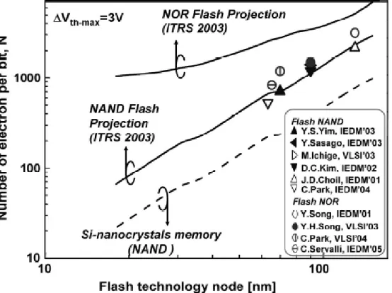
Fig. 1.4 Number of electrons representing a bit as a function of the Flash technology node (only single bit cell are considered), according to the IRTS 2003 edition.
6
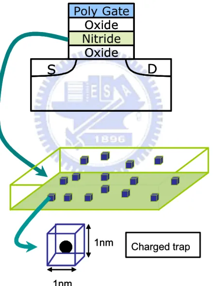
Fig. 2.1 The trap is a cubic with spacing 1nm in nitride layer, and assume a fixed charge Q = -e in a storage trap.
10
Fig. 2.2 Device is controlled by the local minimum-VTregion. 11 Fig. 3.1(a) It indicates a lack of correlation between VTFand VTRof
SONOS at the drain bias Vd = 1V.
18
Fig. 3.1(b) It indicates a lack of correlation between VTFand VTRof SONOS at the drain bias Vd = 0.1V.
19
Fig. 3.2(a) Difference of surface potential landscape between Vd = 0.1V and Vs=0.1V is not obvious.
20
Fig. 3.2(b) Potential of the critical region between Vd= 1.0 V and Vs=1.0 V is very different in microscopic.
21
Fig. 3.3 As L is increased, the probabilities of percolation decreased, since it requires the connection among an increasing number of independent inverted regions.
22
Fig. 3.4 Average VTincreases as the L is increased due to decrease of percolation path.
23
Fig. 3.5(a) . When channel length decreased the magnitude of the fluctuations
increase.
24
Fig. 3.5(b) As dimensions are decreased the magnitude of the fluctuations increase.
25
Fig. 3.6(a) The reduction of Weffalso results in an increase of the threshold voltage fluctuation.
26
Fig. 3.6(b) The reduction of Weffalso results in an increase of the threshold voltage fluctuation.
27
Fig. 3.8 The spreading of VTs (VT) becomes more serious as we increase the programmed charge density.
29
Fig. 3.9 Even thought the spread of VTis increasing with increase of program window, it still have chance to owe the larger operation window.
30
Fig. 3.10 This means that going toward smaller and smaller cell areas, higher and higher program charge density will be needed.
31
Fig. 3.11 Thinner bottom oxide makes the local channel potential more sensitive induced by trapped charge.
32
Fig. 3.12(a) The thinner bottom oxide makes the difference of surface potential between each local channel region is higher than the device with thick bottom oxide
33
Fig. 3.12(b) The thinner bottom oxide makes the more sensitive on threshold voltage fluctuations induced by random program charge distribution effect.
34
Fig. 3.13(a) The higher dielectric constant material can have the tight distribution of program threshold voltage.
35
Fig. 3.13(b) The higher dielectric constant material can have the tight distribution of program threshold voltage.
36
Fig. 4.1 Investigate the influence of discrete dopant in the depletion region.
41
Fig. 4.2(a) A 4-nm-thick lightly doped layer (NA=1015cm-3, background doping concentration) was placed on the substrate surface.
42
Fig. 4.2(b) To use a 4-nm-thick lightly doped layer to replace the heavily doped layer and increase its thickness from the bottom of depletion region to the substrate surface
43
Fig. 4.3 The VTdependence is on the lightly doped layer thickness. 44 Fig. 4.4 The scatter plot represents the relationship between Random
dopant (RD) and random trapped charge (RC) on the threshold voltage fluctuations.
45
Fig. 4.5 Random dopant effect can be suppressed by epitaxial layer with lightly doped concentration.
46
Fig. 4.6 The simulation results are compared with conventional random dopant effect.
Chapter 1
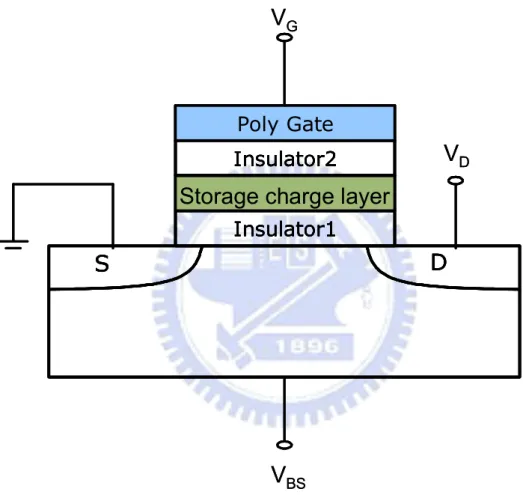
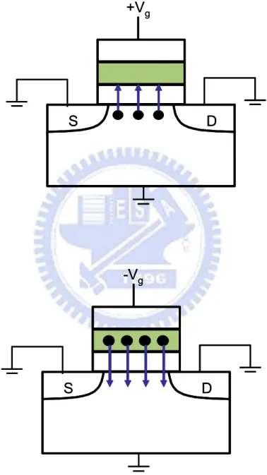
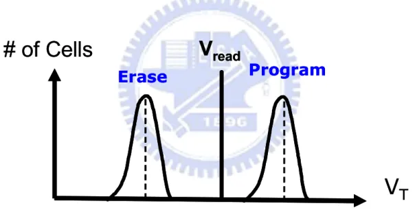
Introduction
The basic operating principle of nonvolatile memory devices is the storage of charges in a material above a MOSFET as depicted in Fig. 1.1. Insulators to prevent the escape of charges usually surround this storage node. If these charges can be put or removed by electrical methods, such as positive Fowler-Nordheim (+FN) (Fig. 1.2 (a)) and negative Fowler-Nordheim (-FN) injections (Fig. 1.2 (b)), the threshold voltage (VT) of the transistor can be modified to switch between two distinct values, and these devices are named as Electrically Erasable Programmable Read-Only Memory (EEPROM). However, as the number of measured cells is increased, the drain current-gate voltage (ID-VG) curve will disperse and the VG under a same read current will spread accordingly. The two distinct values of a device then become two VT distribution sets of a product as shown in Fig. 1.3. Currently, three main storage materials are frequently discussed in literatures. A conventional floating gate device (FG) uses poly-silicon to store its charges while a nitride and Si nano-dots are used in a SONOS and a nano-crystal device, respectively. A critical concern of these cells is the tight control of threshold voltage (VT) within given specifications, especially in multi-level cells (MLC) [1]. The VT distribution further shifts and broadens due to repeated program/ erase cycles and trap assisted tunneling or charge loss during retention [2, 3].
In fresh virgin cells, the VT distribution is generally wide, due to the effects of process variations being amplified upon the shrunken cell geometry [4]. Moreover, according to reference [5], which we copy the figure as Fig. 1.4, the number of electrons representing one
bit dramatically reduces as the dimensions of flash memories are scaled down with increasing memory density. In other words, the VTdistribution of product will show less immunity to the number fluctuation of both dosage counts and stored electrons during scaling. This implies that small perturbations in processing and operation of the cell will give rise to larger VT distributions. Many efforts have been devoted to tightening the VT distribution not only by process optimization but also by correction algorithms [6].
In addition, VTdispersion is also sensitively affected by local effects such as the discrete dopant fluctuation [7], random poly-silicon grain size etc. [8]. Concerning this, silicon nanocrystals (Si-ncs) or SONOS, should suffer worse VT variation than convention FG devices. It has recently been shown that the exclusion zone around Si-ncs obtained by chemical vapor deposition [9] plays a fundamental role in the fluctuations from bit to bit of the dot surface coverage. Similarly, the detailed microscopic program charge arrangement in the nitride layer, which allows the formation of one or few conduction paths connecting the source to drain, is supposed to have non-negligible influences on device electrical performance. Therefore, in this work, we employed a three-dimensional drift-diffusion simulator (ISE) to examine the dependence of the VT on discrete microscopic random distribution/arrangement of the program charges in the nitride layer. The scaling effect will also be studied in such way.
This thesis is organized into five chapters. Following the introduction, flow charts and basic assumptions are detailed described in chapter 2. And then, four main factors including length, width, the dielectric thickness, program window and the random dopant variation will be investigated. Finally, some improved methods and suggestions are given.
Insulator1
Insulator2
Poly Gate
S
D
Storage charge layer
V
GV
DV
BSInsulator1
Insulator2
Poly Gate
S
D
Storage charge layer
Insulator1
Insulator2
Poly Gate
S
D
Insulator1
Insulator2
Poly Gate
S
D
Storage charge layer
V
GV
DV
BS+V
gS
D
+V
gS
D
-V
gS
D
-V
gS
D
Fig. 1.2 Charge injections in nonvolatile memory during (a) +FN write and (b) –FN erase operation
V
T
Program
# of Cells
Erase
V
readV
T
Program
# of Cells
Erase
V
readFig. 1.4 Number of electrons representing a bit as a function of the Flash technology node (only single bit cell are considered), according to the ITRS 2003 edition.
Chapter 2
Simulation Technique
2.1 Devices structure and Simulation Tools
We present TCAD simulations of NAND-type SONOS memories performed with commercial tools, which allow for a good understanding of the impact of the localized charge on electrostatics of the cell. Devices tested in this work are NMOS memory cells with a layer of nitride as trapping layer.
Our simulations are centered on SONOS’s with a channel length Lg = 22 nm to research the end of roadmap in the future. The channel length is defined as gate length. The channel width in most of the simulations is Weff =45 nm. And the doping level of NA =1018cm-3 is required to efficiently suppress the short channel effect around the 22 nm channel length barrier. The bottom, top oxide and nitride layer are with a thickness of 3 nm, 8 nm and 7 nm, respectively. Top and bottom oxide layers are considered as pure potential barrier (no traps), and we neglect the electron to escape from them.
The quantum confinement energy becomes significant when the nanocrystal size shrinks to the nanometer range [10]. Similarly, we use a trap as a cubic with spacing 1nm in nitride layer, and assume a fixed charge Q = -e in a storage trap (Fig. 2.1). The average number of charges in this region is calculated by integrating the continuous charged trap density distribution within it. Program charges with a probability distribution corresponding to the continuous charge distribution are placed randomly in the nitride layer.
2.2 Electrostatic Simulations
three-dimensional, drift- diffusion, which solve self-consistently the Poisson (1) and the carrier continuity equations(2) (3).
ε ψ q p n ND NA (1) n n J qR q t (2) P p J qR q t (3)In our simulation, the threshold voltage is determined by using a current criteria of 10-6Weff/ Lg A . The boundary conditions are V = 0 at the source contact, V = Vdat the drain contact, and zero normal derivative of V at all other boundaries of the solution domain. And our simulations do not include the quantization in the inversion layer and the poly-depletion effect.
2.3 Percolation theory
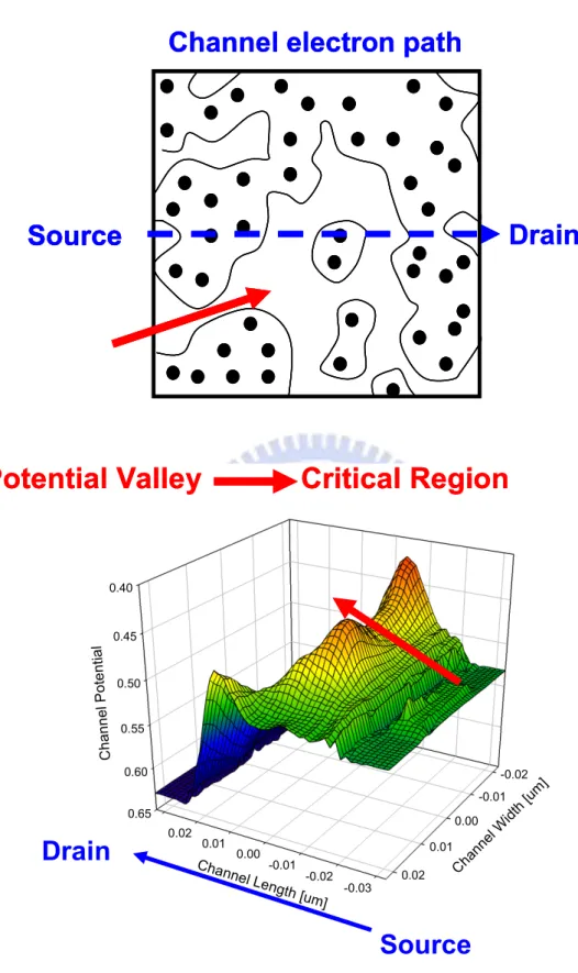
When a negative charge is trapped in the storage node, channel inversion close to the traps is inhibited, whereas positive charging can locally enhance the inversion charge. As a result, the inversion charge in the channel is not uniform, and the concept of threshold voltage must be revisited.
Non-uniform charge distribution changes the local VTin various parts of the device. In the channel width direction, the device may be viewed as many parallel transistors, and the device is controlled by the local minimum-VT region (Fig. 2.2) [11]. This conduction criterion corresponds to a percolation condition, where channel electrons are able to percolate from source to drain through inverted regions. This local minimum-VT region can be considered as the critical percolation bridge connecting the source side to the drain side.
flash memories are scaled down. As a result, the variation in number and position of program charges in the nitride layer makes the microscopic difference between each programmed SONOS more obvious. Most importantly, the random program charge induced inhomogeneous channel potential, inherent to the atomistic simulations, and associated with percolation of the channel current through “valleys”in the potential fluctuations.
2.4 Statistic Method
We adopted the hypothesis that the threshold voltage fluctuations associated with random program charge follow a normal distribution. The standard deviation of the program window for the whole population of microscopically different transistors is
2 T 1 T ( V ) V N Ti i V N
, and the mean value of program window is T
V
. In order
to maintain aclearseparation between the“1”and “0”memory programmed states, we used normalize deviation (σ(VT)/VT) to investigate.
Oxide
Nitride
Oxide
Poly Gate
S
D
1nm
1nm
Charged trap
Oxide
Nitride
Oxide
Poly Gate
S
D
Oxide
Nitride
Oxide
Poly Gate
S
D
1nm
1nm
1nm
1nm
Charged trap
Fig. 2.1 The trap is a cubic with spacing 1nm in nitride layer, and assume a fixed charge Q = -e in a storage trap.
Drain
Channel electron path
Source
Drain
Channel electron path
Source
Source
0.40 0.45 0.50 0.55 0.60 0.65 -0.03 -0.02 -0.01 0.00 0.01 0.02 -0.02 -0.01 0.00 0.01 0.02 C h a n n e lP o te n tia l Channe l Length[um] Ch anne l Wid th[u m]Source
Drain
Potential Valley
Critical Region
Potential Valley
Critical Region
Chapter 3
Statistical Distribution of
VTwith Fixed Program Charge Number
3.1 Introduction
The programming mechanism of NAND-type SONOS flash memory is Fowler- Nordheim (FN) tunneling. The number of electrons representing one bit dramatically reduces as the dimensions of flash memories are scaled down. Thus the characteristic of the discrete charged traps can not be neglected. A complete understanding of the influence of the program charge distribution on threshold voltage fluctuation needs to be built in order to define the specifications and the limits of the device. In order to investigate this effect on the threshold voltage fluctuation, we have evaluated VT asymmetry by interchanging the source and the drain terminals [12]. And both Lg, Weff, program window and dielectric thickness are varied in the different simulation experiments.
3.2 Both forward and reverse source/ drain operation
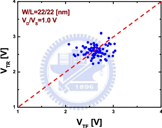
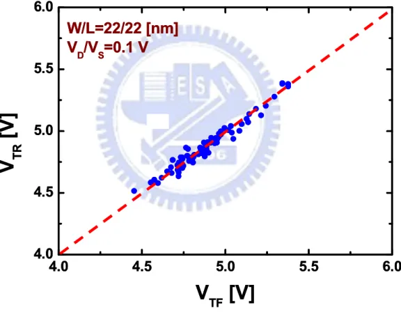
Microscopic program charge distribution gave rise to asymmetry in drain current upon interchange the source and the drain. VTF and VTR show the threshold voltages before and after interchanging the source and the drain terminals, respectively. Fig. 3.1 (a) and (b) show the relationship between VTF and VTR of SONOS at the drain bias Vd of 1 and 0.1 V, respectively, where Lg is about 22 nm. Moreover, the correlation between VTF and VTR becomes degraded at a high drain bias. It should be noted that VTF significantly differs from VTRin the case of Vd = 1 V, but VTFis almost the same as VTRat Vd=0.1 V. This fact means that the threshold voltage has asymmetry on interchanging the source and the drain terminals at a high drain bias, and this asymmetrical V disappears when the drain bias is reduced.
When drain (source) side depletion broadens toward to the direction of channel region, part of program charge region was covered. At that time, VTis affected by the program charge region which is near the source (drain) side.
In Fig. 3.2, the difference of surface potential landscape between Vd= 0.1V and Vs=0.1V is not obvious. For Vd= 1.0 V and Vs=1.0 V, we found the critical region is very different. Therefore, VT asymmetry is considered to be the fact that the program charge arrangement near the drain side and the source side microscopically fluctuate and statistically differ from each others. We can say that this VTasymmetry is caused by the statistical-random distributed program charge in the nitride layer. In other words, VT asymmetry increases with decreasing the effective channel length.
3.3 Channel length dependence of VT
Different probabilities of percolation, depending on the distance between the two electrodes that has to be connected by the percolation path (i.e. L) and on the width of the electrodes (i.e. W). In fact, as the inter-electrode distance L is increased, the probabilities of percolation decreased, since it requires the connection among an increasing number of independent inverted regions (In Fig. 3.3). As expected, the average VTincreases as the L is increased, corresponding to increasingly less probable percolation through inverted regions, as indicated in Fig.3.4.
Fig. 3.5(a) and (b) shows the fluctuations in threshold voltage, VT , for SONOSs scaled from 65nm to 32nm. When channel length continues to increase, the number of independent inversion regions which is needed to connect to percolate from source to drain increase. The more trapped charges make the more critical regions to control percolation. Thus, the effect of charge distribution has abated, and the threshold voltage variation
decreases.
3.4 Channel width dependence of VT
In the channel width direction, the device may be viewed as many parallel transistors and the device is controlled by the local minimum-VT region. Increasing the channel width Weff improves the probability for the percolation by simply increasing the number of possible paths connecting source and drain.
Note that the reduction of Weff also results in an increase of the threshold voltage fluctuation (In Fig. 3.6 (a) and (b)). The influence of one electron is much larger in the narrow channel device, and the electrons in several local minimum-VT regions dominant the conductance of the whole channel. Thus, small number of trapped charges makes each SONOS which one has the same number of program charge very differently (In Fig. 3.7). The increased spread of the VTdistribution can be explained by the typically small number of traps controlling the percolation bottleneck.
3.5 Program charge density dependence of VT
From section 3.3 and 3.4, we can find that the charge number is the main factor to decide the importance of the program charge placement. In this section, we investigate the VTspread in the different program charge density in the cell with the same charnel width Weff =45nm and channel length Lg =45nm. The spreading of VTs (VT) becomes more serious as we increase the programmed charge density (In Fig. 3.8) induced by the increment of the randomness of conduction paths from source to drain should be responsible for this phenomenon.
Even thought the spread of VTis increasing with increase of program window, it still have chance to get the larger operation window (In Fig. 3.9). The higher operation window can
maintain aclearseparation between the “1” and “0”memoryprogrammed states. In Fig. 3.10, we considered SONOS memory cells with channel length 32nm, 45nm with channel width 45nm and channel width 22nm, 45nm with channel length 45nm. In order to maintain a clear separation between the “1” and “0” memoryprogrammed states, we have to assure σ (VT)/VT < 6% on our devices, for whatever combination of cell area and program charge density. The results indicate smaller device needs more program charges to ease the fluctuation of VT induced by random program charge. This means that going toward smaller and smaller cell areas, higher and higher program charge density will be needed, which assures both small dispersion and clearly detached memory states.
3.6 Oxide-nitride-oxide (ONO) stacked layers dependence of VT
3.6.1 Bottom oxide thickness
Important for embedded SONOS memories are the lower program and erase voltages compared to floating gate flash, due to the thin bottom oxide. These low voltages are combined with excellent endurance, but the data retention is an issue [13].
Since surface potential is remotely controlled by trapped charges and a thinner bottom oxide means that a shorter distance from programmed charges to Si-surface, these charges certainly will show a stronger impact on the surface potential than those stored above a thicker oxide. Fig. 3.11 indicates thinner bottom oxide makes the local channel potential more sensitive induced by trapped charge. In other words, the thinner bottom oxide results inhomogeneous channel potential more serious. We used device with Lg=22nm Weff=22nm to investigate how about random charge effect at the same program window with discrete program charge in different bottom oxide thickness (TBOX=1, 3, 5 nm). The decreasing of bottom oxide thickness results in the increasing of spread of threshold voltage (Fig. 3.12). The
thinner bottom oxide makes the more sensitive on threshold voltage fluctuations induced by random program charge distribution effect. In other words, even the total effective oxide thickness (EOT) does not change much during bottom oxide scaling, the VT fluctuation is greatly affected.
3.6.2 Top ON stakes thickness
Usually SiO2 is applied as a top oxide in a conventional SONOS. Since SiO2 has low dielectric constant 3.9 in comparison with Si3N4(7.5) the electric field in top oxide is about two time larger, than in nitride. Therefore, for scaled SONOS device with comparable thickness of nitride and SiO2 top oxide, a remarkable part of applied voltage drops on the top oxide during W/E programming . Replacing SiO2 by high-k dielectric can decrease this undesirable voltage drop and, consequently, the total applied voltage [14].
We used the different top oxide thickness with the EOT of different dielectric constant material (Si3N4 (3.9), Al2O3 (9) and ZrO2 (25)), which have the same physical thickness, to investigate the influence of ON stacks capacitance in threshold voltage fluctuations. According to equation (4)
T 0
V
SiN(
BO N)
BO NQ
x
x
(4) SiNQ is the total amount of the charge trapped in the nitride, are the dielectricBO, N constants in the blocking oxide and nitride. Here, it can be shown that the higher dielectric constant makes the lower EOT of ON stacks. Thus the contribution of one trapped charge in VT deviation is reduced. Even the lower EOT the more number of program charge to represent one bit is needed, the deviation of VT is offset by lower EOT. In Fig. 3.13(a) and (b), the higher dielectric constant material can have the tight distribution of program threshold
voltage. As the results, the top oxide or trapped layer replaced by high-k material can ease the random charge effect.
3.7 Summary
In this chapter, we investigate the cell VTin presence of negatively charged traps is statistically distributed due to the statistical fluctuation of charged trap positions at the trapped layer. For fixed charged trap number, the fluctuation in the trapped charge positions induces a statistical modulation of the local inversion charge in the silicon substrate. For a fixed applied gate voltage, the inversion charge is in fact smaller near the negatively charged traps, reducing the current flow in these regions. Nonuniform channelconduction thusresults,with cellΔVT strictly dependent on the possibility for the trapped charges efficiently stop the current flow from source to drain.
As device is scaled, the VT fluctuation is more serious. The standard deviation increases with decreasing of channel length and width, which illustrates the discrete program charge effect is non-negligible. And the spread of VT is also increasing for cells with
higher program charge density, because the increment of randomness of percolation path. This means that going toward smaller and smaller cell areas, higher and higher program charge density will be needed, which assures both small dispersion and clearly detached memory states. In our knowledge, the program threshold voltage is related with ON stacks capacitance. In this work, we found the random charge effect is not only related with ON capacitance but also bottom oxide thickness.
1 2 3 4 1 2 3 4
W/L=22/22 [nm]
V
D/V
S=1.0 V
V
TR[V
]
V
TF[V]
1 2 3 4 1 2 3 4W/L=22/22 [nm]
V
D/V
S=1.0 V
V
TR[V
]
V
TF[V]
Fig. 3.1(a) It indicates a lack of correlation between VTFand VTRof SONOS at the drain bias V = 1V.
4.0
4.5
5.0
5.5
6.0
4.0
4.5
5.0
5.5
6.0
W/L=22/22 [nm]
V
D/V
S=0.1 V
V
TR[V
]
V
TF[V]
4.0
4.5
5.0
5.5
6.0
4.0
4.5
5.0
5.5
6.0
W/L=22/22 [nm]
V
D/V
S=0.1 V
V
TR[V
]
V
TF[V]
Fig. 3.1(b) It indicates they are highly correlated between VTFand VTRof SONOS at the drain bias Vd=0.1V.
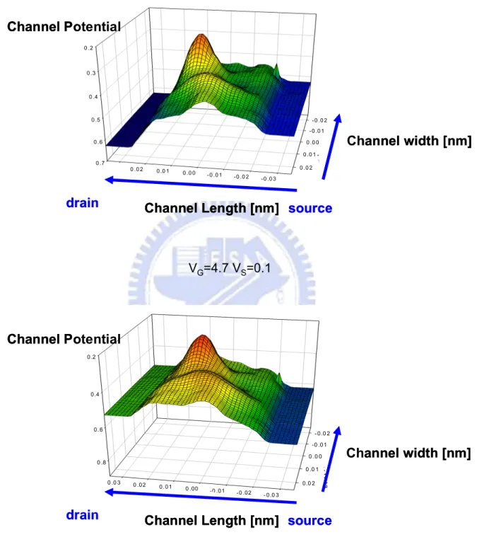
VG=4.7 VS=0.1 VG=4.7 VD=0.1 0 .2 0 .3 0 .4 0 .5 0 .6 0 .7 -0 .0 3 -0 .0 2 -0 .0 1 0 .0 0 0 .0 1 0 .0 2 -0 .0 2 -0 .0 1 0 .0 0 0 .0 1 0 .0 2 X D a ta Y D ata Channel Length [nm] Channel Potential Channel width [nm] source drain 0 .2 0 .3 0 .4 0 .5 0 .6 0 .7 -0 .0 3 -0 .0 2 -0 .0 1 0 .0 0 0 .0 1 0 .0 2 -0 .0 2 -0 .0 1 0 .0 0 0 .0 1 0 .0 2 X D a ta Y D ata Channel Length [nm] Channel Potential Channel width [nm] source drain 0.2 0.4 0. 6 0 .8 - 0.0 3 -0 .02 -0 .01 0 .00 0.01 0 .02 0 .0 3 - 0.0 2 -0 .01 0 .0 0 0 .0 1 0.0 2 X D a ta Y D ata Channel Length [nm] Channel Potential Channel width [nm] source drain 0.2 0.4 0. 6 0 .8 - 0.0 3 -0 .02 -0 .01 0 .00 0.01 0 .02 0 .0 3 - 0.0 2 -0 .01 0 .0 0 0 .0 1 0.0 2 X D a ta Y D ata Channel Length [nm] Channel Potential Channel width [nm] source drain VG=4.7 VS=0.1
Fig. 3.2(a) Difference of surface potential landscape between Vd= 0.1V and Vs=0.1V is not obvious.
0 .0 0 .5 1 .0 1 .5 2 .0 2 .5 -0 .0 3 - 0 .0 2 -0 .0 1 0 .0 0 0 .0 1 0 .0 2 -0 .0 2 -0 .0 1 0 .0 0 0 .0 1 0 .0 2 Z D a ta X D a ta Y D a ta 0 .0 0 .5 1 .0 1 .5 2 .0 2 .5 -0 .0 3 - 0 .0 2 -0 .0 1 0 .0 0 0 .0 1 0 .0 2 -0 .0 2 -0 .0 1 0 .0 0 0 .0 1 0 .0 2 Z D a ta X D a ta Y D a ta Channel Length [nm] Channel Potential Channel width [nm] source drain Channel Length [nm]
Channel Potential Channel width [nm] source drain 0 .0 0 .5 1 .0 1 .5 2 .0 2 .5 -0 .0 3 - 0 .0 2 -0 .0 1 0 .0 0 0 .0 1 0 .0 2 -0 .0 2 -0 .0 1 0 .0 0 0 .0 1 0 .0 2 Z D a ta X D a ta Y D a ta 0 .0 0 .5 1 .0 1 .5 2 .0 2 .5 -0 .0 3 - 0 .0 2 -0 .0 1 0 .0 0 0 .0 1 0 .0 2 -0 .0 2 -0 .0 1 0 .0 0 0 .0 1 0 .0 2 Z D a ta X D a ta Y D a ta Channel Length [nm] Channel Potential Channel width [nm] source drain Channel Length [nm]
Channel Potential Channel width [nm] source drain
Critical region
V
G=3.6 V
S=1.0
0.5 1.0 1.5 2.0 -0.03 -0.02 -0.01 0.00 0.01 0.02 0.03 -0.02 -0.01 0.00 0.01 0.02 Z D a ta X D ata Y D ata 0.5 1.0 1.5 2.0 -0.03 -0.02 -0.01 0.00 0.01 0.02 0.03 -0.02 -0.01 0.00 0.01 0.02 Z D a ta X D ata Y D ata 0.5 1.0 1.5 2.0 -0.03 -0.02 -0.01 0.00 0.01 0.02 0.03 -0.02 -0.01 0.00 0.01 0.02 Z D a ta X D ata Y D ata Channel Length [nm] Channel Potential Channel width [nm] source drain Channel Length [nm]Channel Potential Channel width [nm] source drain 0.5 1.0 1.5 2.0 -0.03 -0.02 -0.01 0.00 0.01 0.02 0.03 -0.02 -0.01 0.00 0.01 0.02 Z D a ta X D ata Y D ata 0.5 1.0 1.5 2.0 -0.03 -0.02 -0.01 0.00 0.01 0.02 0.03 -0.02 -0.01 0.00 0.01 0.02 Z D a ta X D ata Y D ata 0.5 1.0 1.5 2.0 -0.03 -0.02 -0.01 0.00 0.01 0.02 0.03 -0.02 -0.01 0.00 0.01 0.02 Z D a ta X D ata Y D ata Channel Length [nm] Channel Potential Channel width [nm] source drain Channel Length [nm]
Channel Potential
Channel width [nm]
source drain
V
G=3.6 V
D=1.0
Fig. 3.2(b) Potential of the critical region between Vd= 1.0 V and Vs=1.0 V is very different in microscopic.
Length
Width
Length
Width
Fig. 3.3 As L is increased, the probabilities of percolation decreased, since it requires the connection among an increasing number of independent inverted regions.
32
40
48
56
64
3.0
3.2
3.4
Channel Width 45nm
P
ro
gr
am
W
in
do
w
V
T[V
]
Channel Length [nm]
-0.5
0.0
0.5
65nm
45nm
32nm
Channel Width 45nm
Program Charge Density 6x10
19cm
-3P
ro
g
ra
m
V
TD
is
tr
ib
u
ti
o
n
[V
]
Channel Length [nm]
30 40 50 60 70 0.14 0.15 0.16 0.17 0.18
Channel Width 45nm
Program Chagre Density 6x10
19cm
-3
<
V
T>
[V
]
Channel Length [nm]
-0.5
0.0
0.5
P
ro
g
ra
m
V
TD
is
tr
ib
u
ti
o
n
[V
]
Channel Width [nm]
45nm
32nm
22nm
Channel Length 22nm
Program Charge Density 6x10
19cm
-3Fig. 3.6(a) The reduction of Weffalso results in an increase of the threshold voltage fluctuation.
20
30
40
50
0.135
0.150
0.165
0.180
<
V
T>
[V
]
Channel Width [nm]
Channel Length 22nm
Program Chagre Density 6x10
19cm
-3Fig. 3.6(b) The reduction of Weffalso results in an increase of the threshold voltage fluctuation.
Fig. 3.7 Small number of trapped charges results in extremely condition on charge arrangement easily.
-0.6
-0.4
-0.2
0.0
0.2
0.4
0.6
W/L=45/45 [nm]
V
T=4.147
V
T=3.09
V
T=2.186
V
T=1.05
8
6
4
2
P
ro
g
ra
m
V
TD
is
tr
ib
u
tio
n
[V
]
Program Chagre Density [x 10
19cm
-3]
Fig. 3.8 The spreading of VTs (VT) becomes more serious as we increase the programmed charge density
Operating Voltage Window
V
TProgram
# of Cells
Erase
V
readOperating Voltage Window
V
TProgram
# of Cells
Erase
V
readFig. 3.9 Even thought the spread of VTis increasing with increase of program window, it still have chance to owe the larger operation window.
2 4 6 8 0.04 0.06 0.08 0.10 0.12 W/L=22/45 [nm] W/L=45/45 [nm]
<
V
T>
/
V
T[V
]
Program charge density [x10
19cm
-3]
2 4 6 8 0.04 0.06 0.08 0.10 0.12 W/L=22/45 [nm] W/L=45/45 [nm]
<
V
T>
/
V
T[V
]
Program charge density [x10
19cm
-3]
2 4 6 8 0.045 0.060 0.075 0.090 W/L=45/45 [nm] W/L=45/32 [nm]
<
V
T>
/
V
T[V
]
Program charge density [ x10
19cm
-3]
2 4 6 8 0.045 0.060 0.075 0.090 W/L=45/45 [nm] W/L=45/32 [nm]
<
V
T>
/
V
T[V
]
Program charge density [ x10
19cm
-3]
Fig. 3.10 This means that going toward smaller and smaller cell areas, higher and higher program charge density will be needed.
Si channel
Thin bottom oxide
Si channel
Thick bottom oxide
Storage charge
Si channel
Thin bottom oxide
Si channel
Thick bottom oxide
Storage charge
Fig. 3.11 Thinner bottom oxide makes the local channel potential more sensitive induced by trapped charge.
2.0
2.4
2.8
3.2
6.33
6
5.35
N
T[ x10
19cm
-3]
B
ox=5nm
B
ox=3nm
B
ox=1nm
P
ro
g
ra
m
m
ed
V
T
(V
)
Bottom Oxide Thickness
T
ox=8nm T
N=7nm
N
Tvaried ==> same
V
TFig. 3.12(a) The thinner bottom oxide makes the difference of surface potential between each local channel region is higher than the device with thick bottom oxide
1
2
3
4
5
2.0
2.4
2.8
3.2
T
ox=8nm T
N=7nm
N
Tvaried ==> same
V
TP
ro
g
ra
m
m
e
d
V
T[V
]
Bottom Oxide Thickness [nm]
0.12
0.16
0.20
0.24
0.28
Fig. 3.12(b) The thinner bottom oxide makes the more sensitive on threshold voltage fluctuations induced by random program charge distribution effect.
2.4
2.7
3.0
3.3
6
9.368
13.478
N
T[ x10
19cm
-3]
K=25
(EOT=1.25nm)
K=9
(EOT=3.5nm)
K=3.9
(EOT=8nm)
B
ox=3nm T
N=7nm
N
Tvaried ==> same
V
TTop Oxide Thickness
P
rog
ra
m
m
e
d
V
T(V
)
Fig. 3.13(a) The thinner top oxide thickness can have the tight distribution of program threshold voltage.
2
4
6
8
2.0
2.4
2.8
3.2
B
ox=3nm T
N=7nm
N
Tvaried ==> same
V
TP
ro
g
ra
m
m
e
d
V
T[V
]
Top Oxide Thickness [nm]
0.12
0.16
0.20
0.24
0.28
S
ta
n
d
a
rd
D
ev
ia
tio
n
(V
)
Fig. 3.13(b) The thinner top oxide thickness can have the tight distribution of program threshold voltage.
Chapter 4
The Effect of Random trapped charge with Random dopant in Threshold
Voltage Fluctuations
4.1 Introduction
The different sources of intrinsic parameter fluctuations, which can be separated in simulations, will occur simultaneously within a single SONOS. To understand how these fluctuations will interact and to what extent they are statistically independent we have carried out simulations with more than one source of fluctuation present [15]. In this chapter, pairs of fluctuation sources are simulated in order to test their statistical interdependence or possible correlation. The pairs considered included discrete random program charges with discrete random dopants. And we considered (I) number fluctuations and (II) atomistically microscopic distribution in random program charges and random dopants.
4.2 Random Dopant Induced Threshold Voltage Fluctuations
As silicon MOSFET is scaled, the number of dopants is of the order of hundreds in the depletion region (In Fig. 4.1), and below 100 in the inversion layer, for minimum geometry devices. As a result, the detailed microscopic dopant distribution in the MOSFET channel will have non-negligible influences on device electrical performances [16].
The depletion width is 36nm in our device structure. To substantially reduce the computation time, we need to investigate which part is efficient to affect threshold voltage. Our simulation focuses on the 22 nm channel length and channel width, and the doping level is NA=1018cm-3 in the following simulations. First, as shown in Fig.4.2 (a), a 4-nm-thick lightly doped layer (NA=1015cm-3, background doping concentration) was placed on the
substrate surface. Then we continued to increase the thickness of the lightly doped layer thickness (case A). To confirm which part in the substrate contributes effectively to affect threshold voltage, we carried out other simulations. As show in Fig. 4.2 (b), we used a 4-nm-thick lightly doped layer to replace the heavily doped layer and increase its thickness from the bottom of depletion region to the substrate surface (case B).
Fig. 4.3 shows the VT dependence on the lightly doped layer thickness. The VTwas most decreased when lightly doped layer was placed at the surface. However, the decreasing rate of VTbecame slow down when the lightly doped layer was 18nm in both cases. The results in Fig. 4.3 indicate that dopant contributions to VT are not the same through the depletion layer. Thus we chose 15nm depth in the substrate to simulate random dopant effect. The fluctuations are studied using typical samples of 100 atomistically different SONOS. Simulation results agree with [16], the random dopant induced threshold voltage lowering, inherent to the atomistic simulations, (threshold voltage of uniform doping, VT0=2.15 V; average threshold voltage of random dopant simulation, <VT>= 1.927 V, and the standard deviation,
T(RD)
V 0.13198
) .
4.3 Dual Sources of fluctuations
4.3.1 Random dopant (RD) and random trapped charge (RC)
It is important to note that, in realistic devices, the number of program charge in the cell is not constant, as assumed in the simulation results, but is affected by a statistical spread due to the Poisson distribution of charged traps in the nitride layer. In this work, we used random program charge density ( NT=3.33×1019 cm-3 ) to simulate the real condition for SONOS operation. The VT standard deviations are VT(RD) 0.13198 V and
T(RC)
V 0.4876
The standard deviation produced by these two sources of intrinsic parameter fluctuations is VT(RC&RD) 0.48903. The combined effect of two statistically independent variables
on the standard deviation is described by the relation 2 2 1,2 ( 1 2)
[15]. If we use this
expression to combine the standard deviations associated with random program charge and random discrete dopants the combined standard deviation is 0.505 V which is higher than the value obtained from the simultaneous simulation of two fluctuation source (VT(RC&RD)0.48903V). This provides strong additional evidence that these two
sources of intrinsic parameter fluctuation in the SONOS device are statistically dependent. In Fig. 4.4, the spread of VT induced by random charge is higher than random dopant. It indicates the random charge effect is the main source in threshold voltage fluctuations.
4.3.2 Random trapped charge with the method of Suppression random dopant effect
According to reference [17], we have already known the random dopant effect can be suppressed by epitaxial layer with lightly doped concentration (In Fig. 4.5). When the epitaxial layer is relatively thick, the width of the depletion layer in the heavily doped region beneath the epitaxial layer becomes rather small. The holes in the heavily doped region start to screen the charge of the discrete random acceptors in the thin depletion layer, reducing their effect on the threshold voltage fluctuation. In our simulation, the thickness of the epitaxial layer has to be chosen 15nm, which part in the substrate contributes effectively to affect threshold voltage. And the background doping in the epitaxial layer is assumed to be 1015cm-3, and the doping behind it is 1018cm-3.
The simulation results are compared with conventional random dopant effect in Fig. 4.6. It indicates that epitaxial layer can efficiency reduce the threshold voltage fluctuation induced by random dopant. But this method can not significantly reduce the program state threshold
voltage fluctuation because of random trapped charge is the main factor to result in VT variation.
N
A=10
18cm
-3n
+n
+Bulk
N
A=10
15cm
-3A
N
A=10
18cm
-3n
+n
+Bulk
N
A=10
15cm
-3N
A=10
18cm
-3n
+n
+Bulk
N
A=10
15cm
-3A
Fig. 4.2(a) A 4-nm-thick lightly doped layer (NA=1015cm-3 , background doping concentration) was placed on the substrate surface.
N
A=10
18cm
-3n
+n
+Bulk
N
A=10
15cm
-3B
N
A=10
18cm
-3n
+n
+Bulk
N
A=10
15cm
-3B
Fig. 4.2(b) We used a 4-nm-thick lightly doped layer to replace the heavily doped layer and increase its thickness from the bottom of depletion region to the substrate surface
0
10
20
30
40
1.8
2.0
2.2
2.4
2.6
2.8
3.0
Case A
Case B
V
T[V
]
Epitaxial Layer Thickness [um]
1
2
3
4
5
6
7
"Random" N
A+ N
T=0
"Uniform" N
A+ "Random" N
T"Random" N
A+ "Random" N
TN
A=1E18(cm
-3)
N
T=6E19(cm
-3)
N
A=1E18(cm
-3)
N
T=6E19(cm
-3)
N
A=1E18(cm
-3)
N
T=0(cm
-3)
L/W = 22 / 22 (nm)
S
im
u
la
te
d
V
T[V
]
Fig. 4.4 the spread of VT induced by random charge is higher than random dopant. It indicates the random charge effect is the main source in threshold voltage fluctuations.
n
+n
+Bulk
N
A=10
18cm
-3N
A=10
15cm
-3N
Ay
N
A=10
18cm
-3Epi: N
A=10
15cm
-3n
+n
+Bulk
N
A=10
18cm
-3N
A=10
15cm
-3N
Ay
N
A=10
18cm
-3Epi: N
A=10
15cm
-3Fig. 4.5 Random dopant effect can be suppressed by epitaxial layer with lightly doped concentration.
Random
Dopant
Conventional
SONOS device
SONOS device
with epitaxial
layer
Random charge
with Random dopant
σV
T= 0.1319
σV
T= 0.0916
σV
T= 0.48903
σV
T= 0.48204
Random
Dopant
Conventional
SONOS device
SONOS device
with epitaxial
layer
Random charge
with Random dopant
σV
T= 0.1319
σV
T= 0.0916
σV
T= 0.48903
σV
T=
Random
Dopant
Conventional
SONOS device
SONOS device
with epitaxial
layer
Random charge
with Random dopant
σV
T= 0.1319
σV
T= 0.0916
σV
T= 0.48903
σV
T= 0.48204
Random
Dopant
Conventional
SONOS device
SONOS device
with epitaxial
layer
Random charge
with Random dopant
σV
T= 0.1319
σV
T= 0.0916
σV
T= 0.48903
σV
T=
Chapter 5
Conclusion
The correlation between programmed charges and threshold voltage (VT) fluctuations are investigated on a SONOS device. Since the charges of such device are locally trapped in a nitride layer, the current path through the channel region differs from device to device from the statistics point of view and this will lead to deviation in VT and dispersion in program window. The impact of various device parameters has been addressed in this thesis.
According to our simulation, we found that VT fluctuations increase with decreasing in channel length and channel width under fixed amount of trapped charges (NT). These results confirm that statistics problem becomes pronounced as device scales. The spreading of VTs (VT) becomes more serious as we increase the programmed charge density although the ratio between VTandVT(VT/VT) is reduced. The increment of the choice of conduction paths from source to drain should be responsible for this phenomenon. Moreover, varying bottom oxide thickness shows more significant effect than changing top oxide thickness. Since surface potential is remotely controlled by trapped charges and a thinner bottom oxide means that a shorter distance from programmed charges to Si-surface, these charges certainly will show a stronger impact on the surface potential than those stored above a thicker oxide. In other words, even the total effective oxide thickness (EOT) does not change much during bottom oxide scaling, the VT fluctuation is greatly affected. On the other hand, although reducing the top oxide thickness also reducesVT, it is merely due to the reduction of EOT.
In addition, when random dopants are taken into account, the VT variations become even worse. Our simulation results indicate that there is a positive correlation between random charge and random dopant on VT fluctuations. This implies that the two factors are not
independent. By using the method described in [17], random dopant fluctuation can be suppressed by using an epi-taxial layer with a lightly doped Si surface concentration. However, random charge effect itself is still a main fluctuation source induced VTspread.
Reference
[1] B. Eitan, R. Kazerounian, A. Roy, G. Crisenza, P. Cappelletti, and A. Modelli, “MultilevelFlash cellsand theirtrade-offs,” in IEDM Tech.Dig.,1996,pp. 169–172.
[2] J.-D. Lee, J.-H.Choi,D.Park,and K.Kim,“Effectsofinterfacetrap generation and annihilation on the data retention characteristics of Flash memory cells,”IEEE Trans.DeviceMater.Rel.,vol.4,no.1,pp.110–117, Mar. 2004.
[3] N. Mielke, H. Belgal, I. Kalastirsky, P. Kalavade, A. Kurtz, Q. Meng, N. Righos,and J.Wu,“Flash EEPROM threshold instabilitiesdueto charge trapping during program/erasecycling,”IEEE Trans.DeviceMater.Rel.,vol. 4, no. 3, pp. 335–344, Sep. 2004.
[4] G. Molas, D. Deleruyelle, B. De Salvo, G. Ghibaudo, M. Gely, S. Jacob, D. Lafond,and S.Deleonibus,“Impactoffew electron phenomenaon floating-gate memory reliability,”in IEDM Tech.Dig.,2004,pp.877–880. [5] B. Kim, W.-H. Kwon, C.-K. Baek, Y. Son, C.-K. Park, K. Kim, and D. M.
Kim,“Edgeprofileeffectoftunneloxideon erasethreshold voltage distributionsin flash memory cells”,IEEE Trans.Electron Devices, vol. 53, no. 12, pp. 3012–3019, Dec. 2006.
[6] A.Asenov,“Random dopantinduced threshold voltagelowering and fluctuationsin sub 0.1 μm MOSFETs:a3D “atomistic”simulation study”,IEEE Trans.Electron Devices,vol.45,pp.2505–2513, Dec. 1998 [7] T.Ezaki,T.Ikezawa,and M.Hane,“Investigation ofrealisticdopant
fluctuation induced device characteristics variation for sub-100 nm CMOS by using atomistic3D process/devicesimulator”in IEDM Tech.Dig.,2002,pp. 311–314.
[8] S. Muramatsu, T. Kubota, N. Nishio, H. Shirai, M. Matsuo, N. Kodama, M. Horikawa,S.Saito,K.Arai,and T.Okazawa,“Thesolution ofovererase problem controlling poly-Si grain size-modified scaling principles for Flash memory” in IEDM Tech.Dig.,1994,pp.847–850
[9] AchyutKumarDutta“Visiblephotoluminescencefrom Genanocrystal embedded into a SiO2 matrix fabricated by atmospheric pressure chemical vapordeposition”in Apl.Phys.Let.68,1189 (1996);DOI:10.1063/1.115964 Issue Date: February 26, 1996
[10] T. Takagaharaand K.Takeda,“Theory ofthequantum confinementeffecton excitons in quantum dots of indirect-gap materials,”Phys.Rev.B,vol.46,p. 15 578, 1992.
[11] Hang-Ting Lue, Tzu-Hsuan Hsu, Szu-Yu Wang, Yi-Hsuan Hsiao, Erh-Kun Lai, Ling-Wu Yang, Tahone Yang, Kuang-Chao Chen, Kuang-Yeu Hsieh, Rich Liu, Chih-Yuan Lu “Study ofLocalTrapping and STIEdgeEffectson Charge-Trapping NAND Flash”,Electron DevicesMeeting,2007.IEDM 2007. IEEE International 2007, pp.161-164, 2007
[12] Tomohisa Mizuno and Akira Toriumi, ULSI Research Laboratories, Toshiba Corporation, I, Komukai Toshiba-cho, Saiwai-ku, Kawasaki 210, Japan “Experimentalevidenceforstatistical-inhomogeneous distributed dopant
atoms in a Si metal-oxide-semiconductor field-effecttransistor”in J. Apl. Phys.,Volume 77, Issue 7, 1995
[13] Rob van Schaijk a,*, Michiel van Duuren a, Wan Yuet Mei b,
“Oxide–nitride–oxide layer optimisation for reliable embedded SONOS memories”in MicroelectronicEngineering,2004 - Elsevier
[14] Gritsenko,V.A.“Design of SONOS memory transistor for terabit scale EEPROM”,Electron Devicesand Solid-State Circuits, 2003 IEEE Conference, 2003
[15] Gareth Roy, Fikru Adamu-Lema, Andrew R. Brown, Scott Roy and Asen Asenov “Simulation ofCombined SourcesofIntrinsicParameter Fluctuations in a‘real’35 nm MOSFET”Electron Devices,IEEE Transactionson,2003 [16] Hon-Sum Philip Wonga,Yuan Tauraand David J.Franka“Discreterandom
dopant distribution effects in nanometer-scaleMOSFETs”,Microelectronics and Reliability Volume 38, Issue 9, September 1998, Pages 1447-1456
[17] Asenov,A.,Saini,S.“Suppression ofrandom dopant-induced threshold voltage fluctuationsin sub-0.1-μm MOSFET'swith epitaxialand δ-doped channels”Electron Devices,IEEE Transactionson,Volume:46,Issue:8,pp. 1718-1724 ,1999