低介電常數碳氧化矽阻障層與銅金屬整合之電性可靠度研究
64
0
0
全文
(2) 低介電常數碳氧化矽阻障層與 銅金屬整合之電性可靠度研究 Electrical Reliability of Integrating Low-k Silicon-Oxycarbide Barrier Film with Cu Metallization 研 究 生:柯依秀. Student:I-Hsiu Ko. 指導教授:陳茂傑. Advisor:Mao-Chieh Chen. 國 立 交 通 大 學 電子工程學系 電子研究所 碩 士 論 文 A Thesis Submitted to Department of Electronics Engineering & Institute of Electronics College of Electrical Engineering and Computer Science National Chiao Tung University in Partial Fulfillment of the Requirements for the Degree of Master in Electronics Engineering June 2004 Hsinchu, Taiwan, Republic of China.
(3) 低介電常數碳氧化矽阻障層與 銅金屬整合之電性可靠度研究 研究生:柯依秀. 指導教授:陳茂傑 國立交通大學 電子工程學系. 電子研究所碩士班. 摘要 本論文探討三種電漿輔助化學氣相沈積法成長之低介電常數碳氧化矽 (silicon-oxycarbide, SiCO)阻障層與銅金屬整合之電性可靠度。論文首 先探討這些低介電常數介電層的物理特性及其熱穩定性,再利用金屬絕緣 層半導體(MIS)結構來分析他們與銅金屬整合所衍生的電性可靠度問題。吾 人發現這些介電材料隨其組合成分中氧濃度的升高,介電材料的密度、反 射係數和介電常數皆有所降低。這是因為較高的含氧量傾向形成「鳥籠型」 的矽-氧-矽鍵結,導致較為疏鬆的微結構。這三種介電層在經過 30 分鐘 500 ℃的熱退火處理後,均展現極佳的高溫熱穩定性。在 500oC以上溫度的高溫 退火後,則由於水氣的熱脫附,使介電常數有所下降。在電性的探討方面, 吾人發現TaN/Cu/SiCO/Si電容結構經過 30 分鐘 400℃的熱退火處理後,在 室溫下測量的漏電流都沒有改變,顯示這三種介電層在沒有外加電場的情 o. 況下,即使在 400 C的高溫也能有效延緩銅的穿透。吾人亦以電容結構研究. i.
(4) 室溫下的漏電流機制,發現隨著電場的增強,導電機制由低電場時的歐姆 傳遞,轉變成Frenkle-Poole發射,然後在高於 0.36 MV/cm電場時發生electric breakdown等三種機制。 再者,吾人利用加溫偏壓法(BTS)施加於TaN/Cu/SiCO/Si及Al/SiCO/Si 電容結構, 迫使銅加速擴散至介電層,藉以探討低介電常數碳氧化矽的電 性可靠度。測試結果顯示,介電層SiCO-A具備優越的抗銅擴散能力以及熱 o. 穩定性,在溫度 200 C電場強度 1 MV/cm的BTS測試 15 小時後,仍能維持原 有的漏電流大小。介電層SiCO-B在相同條件的BTS測試 15 小時, 鋁電極的 電容展現良好熱穩定性,漏電流維持不變,然而銅電極的電容在BTS測試的 16 分鐘內即全數崩潰,推測是由於SiCO-B的鳥籠型微結構較為疏鬆,無法 阻擋銅的擴散之故。此外.介電層SiCO-C由於介電質本身的強度過於脆弱, o. 即使鋁電極的電容在 200 C施加 1MV/cm電場強度的BTS下很快便崩潰,而銅 o. 電極的電容則無法在 200 C支撐過 0.8 MV/cm電場強度的測試。 總結本論文之研究結果顯示 k 值約為 4 的碳氧化矽 SiCO-A 具有極佳的 抗銅性與熱穩定性,是極具潛力的銅鑲嵌製程之介電阻障材料,有機會取 代目前通用的高介電常數之氮化矽(k~7),應用於銅鑲嵌製程。. ii.
(5) Electrical Reliability of Integrating Low-k Silicon-Oxycarbide Barrier Film with Cu Metallization Student: I-Hsiu Ko. Advisor: Mao-Chieh Chen. Department of Electronics Engineering & Institute of Electronics National Chiao Tung University. Abstract This thesis studies the thermal stability and physical property for three PECVD low-k (k-value less than 4) amorphous silicon-oxycarbide (α-SiCO:H) dielectric barrier films with different elemental compositions designated as SiCO-A (SiC1.19O0.73), SiCO-B (SiC1.12O0.77) and SiCO-C (SiC1.34O0.85).. More. importantly, this study also explores the electrical reliability of integrating these silicon-oxycarbide dielectric barrier films with Cu metallization using planar MIS capacitor structure. It is found that the film density, dielectric constant and refractive index all decrease with increasing content of oxygen in the dielectric composition; this is presumably because higher content of oxygen tends to make the Si-O-Si bond of the dielectrics forming a cage-like bonding, which is a relatively loose microstructure.. All of the three dielectrics are. thermally stable up to 500oC (in N2 ambient for 30 min).. However, the. dielectric constant of the α-SiCO:H films decreases slightly at temperatures above 500oC because the H2O outgassing at the elevated temperatures would iii.
(6) diminish the ionic and dipolar polarization, and thus the dielectric constant. Leakage current of the dielectrics at room temperature exhibited different conduction mechanisms at different electric fields, including ohmic conduction at very low electric fields, Frenkle-Poole emission at low electric fields, and electric breakdown generally at electric fields above 0.36 MV/cm.. All the. three α-SiCO:H dielectric films are presumably capable of retarding Cu diffusion at temperatures up to 400oC without an applied electric field because no difference in room temperature leakage current was observed between the Al-gated and TaN/Cu-gated MIS capacitors, whether as-fabricated or 400oC-annealed.. The SiCO-A dielectric film exhibited a good dielectric barrier. property against Cu penetration; its MIS capacitors were able to withstand BTS at 200℃ under 1 MV/cm electric field up to at least 15h.. This indicates that. the SiCO-A dielectric is a potential candidate to replace the higher dielectric constant SiN film as a Cu-cap barrier and etching stop layer in the Cu damascene structure.. The SiCO-B dielectric, presumably due to its loose and. more cage-like Si-O-Si bonding structure, can not prevent Cu from diffusion into the film under the BTS (at 200oC with 1 MV/cm electric field).. The. SiCO-C dielectric has an even weaker dielectric strength; in fact, breakdown occurred to the 400oC-annealed TaN/Cu/SiCO-C/Si MIS capacitor under an electric field of 0.8 MV/cm at 200oC.. iv.
(7) 誌謝 這是我最珍貴的青春年華,「只為你如花美眷,似水流年…」; 然而我不在幽閨自憐,兩年來在交大女二舍、工四館、NDL盡情追尋 自我實現,或者回南投竹山的家偷得浮生半日閒;期間有咬牙的苦、 更多學習的甜,我會永遠懷念。 感謝陳茂傑教授,在兩年碩士班期間指引我方向,又給予我信任 與自由。老師治學嚴謹負責,指導學生卻總是理直氣和、從不疾言厲 色。有幸拜入老師門下,除了學業研究上的指點,這謙謙君子的大師 風範也讓學生有所體悟。感謝吳偉豪、王超群和吳振誠學長在這兩年 中的指導與協助,對我而言豪哥認真的身影已是 629 的必要風景,宛 如燈塔般的指引;謝謝林信宏、王安志、楊宇國同學的陪伴支持與實 驗上的幫忙,信宏的熱心負責讓我此後非常喜歡成大的學生,而安志 的樂天總能讓我舒緩緊張。我在此要向蔣秋志學長致上最誠摯的謝 意,學長花時間訓練我實驗機台,花心思安排實驗規劃,還要花上許 多耐心,讓我把他當作中文發音還附上詳盡註解的 IEEE Xplore、排 除疑難小幫手。秋志學長是值得信賴的智者,也是可以互相吐槽的朋 友;多功能、全自動,是我求學生涯的貴人與良友,沒有學長的指導 與幫忙就不會有這篇論文。最後感謝我的父母、哥哥給我親情溫暖; 感謝曾逸晨先生一路上的支持與陪伴,逸晨,謝謝。. v.
(8) Contents Abstract (Chinese) ……………………………………………………… i Abstract (English)………………………………………………………… iii Acknowledgement ……………………………………………………… v Contents…………………………………………………………………… vi Table Captions …………………………………………………………… viii Figure Captions…………………………………………………………… ix Chapter 1. Introduction 1.1 General Background …………………………………… 1 1.2 Motivation and Material Options……………………… 2 1.3 Thesis Organization……………………………………… 3 Chapter 2. Physical Property and Thermal Stability of α-SiCO:H Films 2.1 Introduction ……………………………………………… 4 2.2 Experimental Procedures ……………………………… 4 2.3 Results and Discussion ………………………………… 6 2.4 Summary ………………………………………………… 10 Chapter 3. Electrical Characteristics of α-SiCO:H Films 3.1 Introduction ……………………………………………… 11. vi.
(9) 3.2 Experimental Procedures ……………………………… 12 3.3 Results and Discussion………………………………… 13 3.4 Summary ………………………………………………… 20 Chapter 4. Conclusion ………………………………………………… 22 References. vii.
(10) Table Captions Table 2-1. Physical Properties of α-SiCO:H Dielectric Films.. Table 2-2. Absorption bonds observed for α-SiCO:H.. Table 2-3. Contribution part of dielectric constant.. viii.
(11) Figure Captions Chapter 1 Figure 1-1 Gate and interconnection delays as a function of devices feature size. Figure 1-2 Electromigration performance improvement using Cu metallization. Figure 1-3 Schema of Cu dual damascene structure.. Chapter 2 Figure 2-1 Process flow of Al/SiCO/Si MIS capacitor preparation. Figure 2-2 FTIR absorption spectra of the α-SiCO:H dielectrics studied in this work. Figure 2-3 The illustration of network and cage-like Si-O-Si structure of SiCO dielectric films. Figure 2-4 TDS of H2O (m/e=18) for the dielectric films of SiCO-A, SiCO-B and SiCO-C. Figure 2-5 TDS of CH4 (m/e=16), N2H+ (m/e=29), C2H6 (m/e=30), O2 (m/e=32), and CO2 (m/e=44) for the dielectric films of (a) SiCO-A, (b) SiCO-B, and (c) SiCO-C. Figure 2-6 Percentage of thickness change vs. annealing temperature for the dielectric films of (a) SiCO-A, (b) SiCO-B, and (c) SiCO-C. Figure 2-7 Refractive index vs. annealing temperature for the three α-SiCO:H dielectric films studied in this work. Figure 2-8 Dielectric constant vs. annealing temperature for the three α-SiCO:H dielectric films studied in this work. ix.
(12) Chapter 3 Figure 3-1 Process flow for the preparation of TaN/Cu/SiCO/Si MIS capacitors. Figure 3-2 Process flow for the preparation of Al/SiCO/Si MIS capacitors. Figure 3-3 Leakage current density vs. electric field measured at room temperature for the as-fabricated and 400oC-annealed Al-gated and TaN/Cu-gated MIS capacitors of dielectric films (a) SiCO-A, (b) SiCO-B, and (c) SiCO-C. Figure 3-4 Leakage current density vs. electric field measured at room temperature for the 400oC-annealed Al-gated and TaN/Cu-gated MIS capacitors of dielectric films SiCO-A, SiCO-B and SiCO-C. This figure is replotted from Fig. 3-3 only for the part of electric field below 0.7 MV/cm. Figure 3-5 Mapping of conduction mechanism for 400oC-annealed Al-electrode capacitors of (a) SiCO-A, (b) SiCO-B, and (c) SiCO-C dielectrics at room temperature. Figure 3-6 Time-dependent dielectric breakdown (TDDB) for 400oC-annealed Al/SiCO-A/Si and TaN/Cu/SiCO-A/Si MIS capacitors under BTS at 200oC with an electric field of 1 MV/cm. Figure 3-7 Leakage current density vs. electric field measured at 200oC for (a) Al/SiCO-A/Si and (b) TaN/Cu/SiCO-A/Si MIS capacitors before and immediately after a 15 h BTS at 200oC with an electric field of 1 MV/cm. Figure 3-8 Time-dependent dielectric breakdown (TDDB) for 400oC-annealed Al/SiCO-B/Si and TaN/Cu/SiCO-B/Si MIS capacitors under BTS at 200oC with an electric field of 1 MV/cm. x.
(13) Figure 3-9. Leakage current density vs. electric field measured at 200oC for (a) Al/SiCO-B/Si and (b) TaN/Cu/SiCO-B/Si MIS capacitors before and immediately after the BTS at 200oC with an electric field of 1 MV/cm.. Figure 3-10. Time-dependent dielectric breakdown (TDDB) for the 400oC-annealed Al/SiCO-C/Si MIS capacitor under BTS at 200oC with an electric field of 1MV/cm.. Figure 3-11. Leakage current density vs. electric field measured at 200oC for the 400oC-annealed TaN/Cu/SiCO-C/Si sample without subjected to any BTS.. Figure 3-12. Statistical distribution of time-to-breakdown for the Al-gated and Ta/Cu-gated MIS capacitors of the three dielectric films under BTS at 200oC with 1MV/cm electric field.. xi.
(14) Chapter 1 Introduction. 1.1 General Background The device dimensions are continuously scaled down with the progress of integrated circuits technology. Smaller devices have a higher operation speed, higher packing density, and lower power consumption. However, when the devices feature size is scaled down toward 0.18µm and beyond, the chip total delay begins to increase, as shown in Fig. 1-1.. Obviously, the shrinking of the. device is not meaningful if the problem of the signal propagation delay can not be overcome [1-2]. The chip total delay consists of intrinsic gate delay and interconnection delay. Unlike the intrinsic gate delay, which can be improved with reduced gate length, scaled interconnects suffer from increased RC delay and tend to dominate the chip performance.. The higher resistance (R) of narrower metal. lines and higher capacitance (C) between more tightly spaced interconnects result in larger RC time delay.. Furthermore, reduced interconnect cross-. sectional area may also lead to higher current density which aggravates electromigration. In order to minimize the RC time delay, two approaches can be taken.. The first approach is to reduce the electrical resistivity in the metal 1.
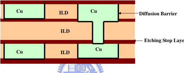
(15) line.. Consequently it is necessary to use other metal material of lower. resistivity to replace the conventional Al-based wires for multi-level interconnection.. Copper (Cu) is an appropriate alternative because of its lower. resistivity (1.7µΩ-cm), as compared with that of aluminum (2.7µΩ-cm).. In. addition, Cu is more resistant to electromigration, which is a vital issue in reliability, as shown in Fig. 1-2 [3].. The second approach is to use low. dielectric constant (low-k) materials as the inter- and intra-layer dielectrics (ILD).. The performance advantage of using Cu lines and low-k dielectric. material is highlighted in Fig. 1-1.. 1.2 Motivation and Material Options In recent years, Cu has been used to replace Al and its alloys as wiring material in multilevel interconnection because of its lower electrical resistivity and superior electromigration resistance. Since it is difficult to pattern a Cu film by plasma etching, dual damascene structure is commonly used for Cu multilevel interconnection.. However, Cu tends to diffuse into ILD under the. influence of electrical and thermal stresses during fabrication process and/or circuits operation, resulting in large leakage current and premature dielectric breakdown.. To prevent Cu from diffusion into ILD, Cu must be sealed by. diffusion barriers and etching stop layers.. Figure 1-3 shows a typical Cu. interconnect dual damascene structure. Silicon nitride (SiN) with a relatively high dielectric constant (~7) is currently used as a standard etching stop layer 2.
(16) since it has been employed as a mask and passivating layer against diffusion of metal and moisture uptake for a long time.. Thus, it is desirable to replace. silicon nitride with some other dielectric barrier materials with lower dielectric constant to further reduce the effective dielectric constant of the Cu interconnect system.. Recently, a newly-developed dielectric barrier material, a low-k. amorphous silicon oxycarbide (α-SiCO:H) film deposited by plasma enhanced chemical vapor deposition (PECVD), has received a great deal of attention [4-8]. In fact, it has been regarded as a promising candidate to replace SiN as the dielectric diffusion barrier and etching stop layer in Cu damascene structure. This thesis is to investigate the physical and barrier properties of three low-k αSiCO:H dielectric films with different composition.. 1.3 Thesis Organization This thesis consists of four chapters.. Following the introduction in. chapter 1, the physical property and thermal stability of the low-k α-SiCO:H dielectric films are investigated and presented in chapter 2.. Chapter 3 deals. with the electrical characteristics and barrier property of the low-k α-SiCO:H dielectric films.. Finally, chapter 4 gives the conclusion of this thesis study.. 3.
(17) Number of Standard Deviations. Cumulative Failures (%). Fig. 1-1 Gate and interconnection delays as a function of devices feature size [1].. AlCu 1X Cu 10X Lifetime. 10. 100. 1000. Time to Failure (Arbitrary Units). Fig. 1-2 Electromigration performance improvement using Cu metallization [3]..
(18) Cu. ILD. Cu. Diffusion Barrier. ILD Etching Stop Layer Cu. ILD. Cu. Fig. 1-3 Schema of Cu dual damascene structure..
(19) Chapter 2 Physical Property and Thermal Stability of α-SiCO:H Films. 2.1 Introduction To enhance the circuit performance in high-speed 90/65 nm CMOS device operations, it is urgent to replace the high-k SiN barrier in Cu dual damascene interconnections with a relatively low-k dielectric barrier film.. In recent years,. many studies have been reported on low-k amorphous silicon oxycarbide (α-SiCO:H) films deposited by plasma enhanced chemical vapor deposition (PECVD) [9-11].. This chapter investigates the physical property and thermal. stability of three PECVD α-SiCO:H dielectric films with different composition.. 2.2 Experimental Procedures The α-SiCO:H films were deposited at temperatures of 200-500oC using organosilicate and oxidation gases with various flow ratios, resulting in three α-SiCO:H films with different compositions designated as SiCO-A, SiCO-B and. 4.
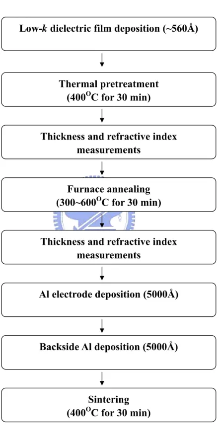
(20) SiCO-C.. The α-SiCO:H dielectric films were all deposited on p-type,. (100)-oriented 12-inch silicon wafers to a thickness of 560 Å in a standard PECVD system at Taiwan Semiconductor Manufacturing Company (TSMC).. All films. deposited were thermally annealed at 400oC for 30 min in an N2 ambient to remove moisture possibly absorbed in the dielectrics.. After this thermal pretreatment, the. film thickness and refractive index were measured by a well-calibrated n&k analyzer at 633 nm wavelength. Subsequently, the films were further annealed in furnace at temperatures from 300 to 600oC for 30 min in an N2 ambient, followed by measurements of film thickness and refractive index. In order to determine the dielectric constant of the α-SiCO:H dielectric films, Al/SiCO/Si MIS capacitors were prepared for capacitance-voltage (C-V) measurements.. The MIS capacitors. were constructed by depositing a 5000-Å-thick Al layer directly on the α-SiCO:H dielectric surfaces using a thermal evaporation system.. The Al electrodes with a. circular area of 0.84 mm diameter were defined by chemical wet etching.. To. ensure good contact in electrical measurement, a 5000-Å-thick Al layer was also thermally evaporated on the back surface of the Si substrate for all samples.. The. completed MIS samples were sintered at 400oC for 30 min in an N2 ambient. Figure 2-1 shows the process flow of the MIS samples preparation. X-ray photoelectron spectroscopy (XPS) using Al Kα (1486.6eV) radiation was used to detect the chemical composition of the α-SiCO:H dielectric films.. 5.
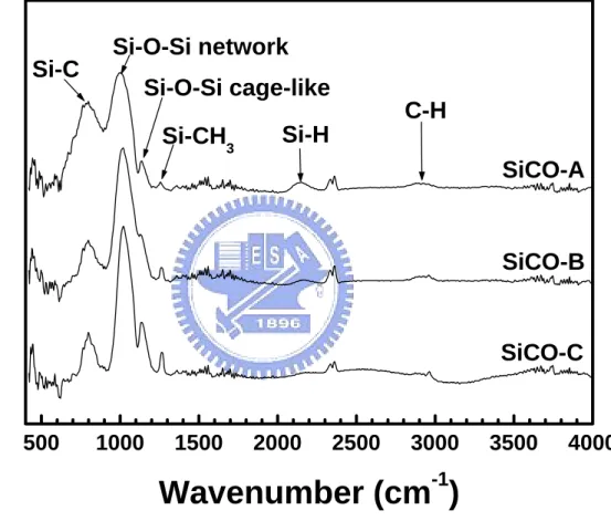
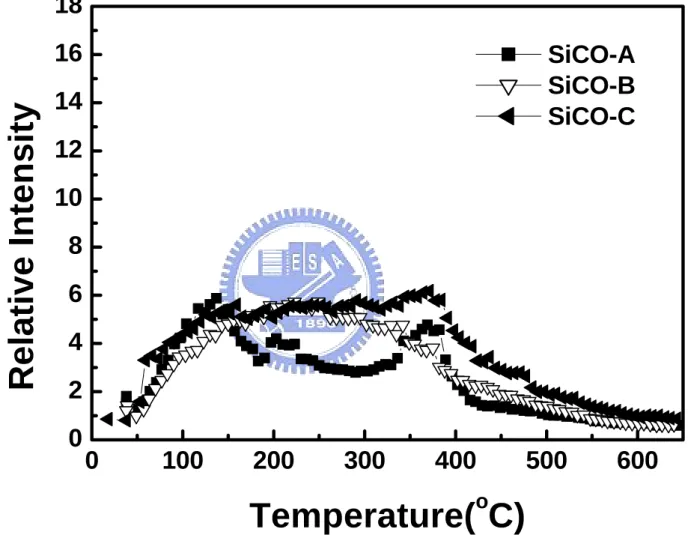
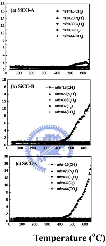
(21) Fourier transform infrared spectroscopy (FTIR) was used to investigate the chemical bonds of the dielectric films.. Thermal desorption mass spectroscopy. (TDS) was used to monitor the outgassing behavior of the dielectrics at elevated temperatures.. The dielectric constant of the α-SiCO:H films was determined from. the maximum accumulation capacitance of the Al-electrode MIS capacitors measured at 1 MHz using a Keithley 82 C-V measurement system.. The film. density was calculated by the ratio of mass to volume of the film, whereas the film mass was measured by electronic balance and the film volume was calculated from the film thickness and the area of the substrate wafer.. 2.3 Results and Discussion Table 2-1 shows the basic physical properties of the α-SiCO:H dielectrics studied in this thesis.. The dielectric constant of the α-SiCO:H dielectric films. decreases with increasing oxygen concentration in the films.. The refractive index,. and the film’s density as well, also shows the same changing tendency. Meanwhile, the carbon content appears to have little effect on the k-value and refractive index of the dielectric films. Figure 2-2 shows the FTIR absorption spectra for the three α-SiCO:H films studied in this work, while Table 2-2 summarizes in detail all the chemical bonding observed and reported in the literature [12-17].. The Si-O-Si bonds of long chain polymers have two strong 6.
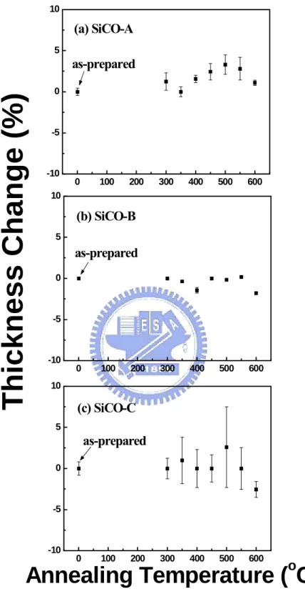
(22) bonds at 1041 and 1128 cm-1, which represent network and cage-like structures, respectively. Figure 2-3 illustrates the network and cage-like Si-O-Si structure of SiCO dielectric films [18-19].. Films that consist of more Si-O-Si cage-like. structure become looser and can therefore have lower dielectric constants as well as refractive indices and films’ densities.. However, films that have too much Si-O-Si. cage-like structure may become too loose to resist Cu diffusion. Figure 2-4 illustrates the TDS of H2O (m/e=18) for the three α-SiCO:H dielectric films, all of which exhibited moisture outgassing.. The TDS of CH4. (m/e=16), N2H+ (m/e=29), C2H4 (m/e=30), O2 (m/e=32), and CO2 (m/e=44) are illustrated in Fig. 2-5.. It was found that only N2H+ (m/e=29) could be detected for. SiCO-B and SiCO-C films at temperatures above 500oC, presumably due to the H+ outgassing [20]. Figure 2-6 shows the percentage of thickness change versus annealing temperature for the three α-SiCO:H dielectric films studied in this work. Each datum was obtained by measurements on a sample at 5 different locations. The as-prepared sample stands for the samples which had been thermally annealed at 400oC (for 30 min in N2 ambient) immediately after the film deposition. All of the three dielectric films are thermally stable up to 500oC. Figure 2-7 shows the refractive index versus annealing temperature for the α-SiCO:H dielectric films.. We found that the refractive index remained virtually. unchanged after thermal annealing at temperatures up to 600oC for all three. 7.
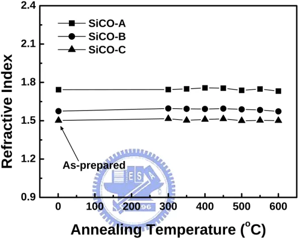
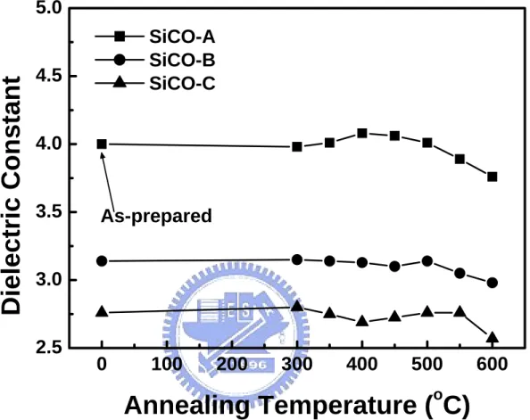
(23) α-SiCO:H dielectric films studied in this thesis.. The dielectric constant versus. annealing temperature is illustrated in Fig. 2-8 for the three α-SiCO:H dielectric films.. It appears that the dielectric constant (i.e. k-value) exhibits a slightly. decreasing tendency at temperatures above 500oC.. It is well known that the. dielectric constant of a dielectric material is an intrinsic material property; it is frequency dependent and is composed of three components: electronic, ionic and dipolar polarization [21].. The dielectric constant can be quantified by Equations. (2-1) and (2-2):. εr (@ 1 MHz) =1 + ∆εe +∆εi +∆εd. (2-1). εr (λ) =n2 (λ). (2-2). where εr is the relative dielectric constant; ∆εe, ∆εi and ∆εd are the contribution from the electronic, ionic and dipolar polarization, respectively, and n2 (λ) is the real part of the refractive index at the wavelength λ.. If λ of the light source is in the visible. to UV range, e.g. λ=633 nm, only electrons can response to the time varying field and the dielectric constant in this range is only due to the electronic polarization. Therefore we can calculate the electronic polarization contribution as follows:. 8.
(24) 1 + ∆εe = n2 (@ 633 nm). (2-3). Moreover, the ionic and dipolar polarization contribution can be obtained by the following:. ∆εi +∆εd = εr (@ 1 MHz) - n2 (@ 633 nm). (2-4). Table 2-3 lists the dielectric constants measured at 1 MHz (1 + ∆εe +∆εi +∆εd), the share (1 + ∆εe) measured by n2 (@ 633 nm), and the extracted ionic and dipolar polarization contribution (∆εi +∆εd) at various temperatures.. The electronic. polarization contribution (∆εe) remains unchanged at temperatures up to 600oC since the refractive index measured is not dependent on the annealing temperature. However, the ionic and dipolar polarization contribution decreases with annealing temperature at temperatures above 500oC.. Since the TDS reveals moisture. outgassing for all samples to various degrees (Fig. 2-4) while no obvious outgassing of CH4 was detected (Fig. 2-5), the moisture would be reduced while the hydrocarbon remained unchanged in the α-SiCO:H dielectric films thermally annealed at temperatures up to 600oC.. Since H2O is more polarizable than CH4,. the ionic and dipolar polarization contribution would decrease with increasing annealing temperature, leading to the decrease of dielectric constant when the. 9.
(25) temperature was raised above 500oC. It can be seen from Fig. 2-5 and Table 2-3 that the H+ outgassing for the SiCO-B and SiCO-C dielectric films at temperatures above 500oC could barely affect the ionic and dipolar polarization contribution.. 2.4 Summary It was found that the α-SiCO:H dielectrics with higher oxygen concentration contain more cage-like structure, which is structurally looser than the network structure.. Thus, the α-SiCO:H dielectric films with higher oxygen concentration. have a lower density as well as lower dielectric constant and refractive index.. All. of the three α-SiCO:H dielectric films studied in this thesis are thermally stable at temperatures up to 500oC.. Nonetheless, the dielectric constant of the α-SiCO:H. dielectric films decreases slightly at temperatures above 500oC; this is attributed to the decrease of the ionic and dipolar polarization at the elevated temperatures due to the outgassing of H2O.. 10.
(26) Table 2-1 Physical Properties of α-SiCO:H Dielectric Films. Sample ID Elemental Composition (%). SiCO-A. SiCO-B. SiCO-C. Si. 34.296. 34.632. 31.369. C. 40.778. 38.744. 41.908. O. 24.926. 26.624. 26.723. Chemical Composition. SiC1.19O0.73 SiC1.12O0.77 SiC1.34O0.85. Density (g/cm3). 1.84. 1.65. 1.56. Dielectric Constant @ 1 MHz. 4.00. 3.14. 2.76. Refractive Index @ 633 nm. 1.743. 1.575. 1.502.
(27) Table 2-2 Absorption bonds observed for α-SiCO:H [9-14].. Wavenumber (cm-1). Vibration mode. 780. Si-C stretching. 800. Si-C bending. 1041. Si-O-Si network bending/stretching. 1128. Si-O-Si cage-like bending/stretching. 1245. Si-CH3 bending. 2140. Si-H streching. 3000. C-H stretching.
(28) Table 2-3 Contribution part of dielectric constant. Dielectric Annealing 1+Δεe +Δεi+Δεd 1+Δεe Δεi+Δεd Films Temperature k (@ 1 MHz) n2 (@ 633 nm) k-n2 (oC) SiCO-A *As 4.00 3.04 0.96 300 3.98 3.04 0.96 350 4.01 3.06 0.95 400 4.08 3.09 0.99 450 4.06 3.08 0.98 500 4.01 3.02 0.99 550 3.89 3.06 0.83 600 3.76 3.00 0.76 SiCO-B. *As 300 350 400 450 500 550 600. 3.14 3.15 3.14 3.13 3.10 3.14 3.05 2.98. 2.48 2.55 2.54 2.53 2.54 2.52 2.51 2.47. 0.66 0.60 0.60 0.60 0.56 0.62 0.54 0.51. SiCO-C. *As 300 350 400 450 500 550 600. 2.76 2.80 2.75 2.69 2.73 2.76 2.76 2.57. 2.26 2.30 2.26 2.28 2.30 2.25 2.26 2.25. 0.50 0.50 0.49 0.41 0.43 0.51 0.50 0.32. * The sample “As” stands for “as-prepared sample” which had been thermally annealed (i.e. thermally pretreated) at 400oC (for 30 min in N2 ambient) immediately after the film deposition..
(29) Low-k dielectric film deposition (~560Å). Thermal pretreatment (400OC for 30 min). Thickness and refractive index measurements. Furnace annealing (300~600OC for 30 min). Thickness and refractive index measurements. Al electrode deposition (5000Å). Backside Al deposition (5000Å). Sintering (400 C for 30 min) O. Fig. 2-1 Process flow of Al/SiCO/Si MIS capacitor preparation..
(30) Si-O-Si network Si-C. Si-O-Si cage-like. Absorbance. C-H Si-CH3. Si-H SiCO-A. SiCO-B. SiCO-C. 500. 1000. 1500. 2000. 2500. 3000. 3500. 4000. -1. Wavenumber (cm ) Fig. 2-2 FTIR absorption spectra of the α-SiCO:H dielectrics studied in this work..
(31) Fig. 2-3 The illustration of network and cage-like Si-O-Si structure of SiCO dielectric films [15]..
(32) 18. Relative Intensity. 16. SiCO-A SiCO-B SiCO-C. 14 12 10 8 6 4 2 0. 0. 100. 200. 300. 400. 500. o. Temperature( C) Fig. 2-4 TDS of H2O (m/e=18) for the dielectric films of SiCO-A, SiCO-B and SiCO-C.. 600.
(33) 18. (a) SiCO-A. 16. m/e=16(CH4) +. 14. m/e=29(N2H ). 12. m/e=30(C2H6). 10. m/e=32(O2) m/e=44(CO2). 8 6 4 2 0. 0. 100. 200. 300. 400. 500. 600. 18. (b) SiCO-B. 16. m/e=16(CH4) +. 14. m/e=29(N2H ). 12. m/e=30(C2H6). 10. m/e=32(O2) m/e=44(CO2). 8 6 4 2 0. 0. 100. 200. 300. 400. 500. 600. 18. (c) SiCO-C. 16. m/e=16(CH4) +. 14. m/e=29(N2H ). 12. m/e=30(C2H6). 10. m/e=32(O2) m/e=44(CO2). 8 6 4 2 0. 0. 100. 200. 300. 400. 500. 600. Temperature (oC) Fig. 2-5 TDS of CH4 (m/e=16), N2H+ (m/e=29), C2H6 (m/e=30), O2 (m/e=32), and CO2 (m/e=44) for the dielectric films of (a) SiCO-A, (b) SiCO-B, and (c) SiCO-C..
(34) 10. (a) SiCO-A 5. Thickness Change (%). as-prepared 0. -5. -10. 0. 100. 200. 300. 400. 500. 600. 300. 400. 500. 600. 300. 400. 500. 600. 10. (b) SiCO-B 5. as-prepared 0. -5. -10. 0. 100. 200. 10. (c) SiCO-C 5. as-prepared 0. -5. -10. 0. 100. 200. o. Annealing Temperature ( C) Fig. 2-6 Percentage of thickness change vs. annealing temperature for the dielectric films of (a) SiCO-A, (b) SiCO-B, and (c) SiCO-C..
(35) 2.4 SiCO-A SiCO-B SiCO-C. Refractive Index. 2.1. 1.8. 1.5. 1.2. 0.9. As-prepared. 0. 100. 200. 300. 400. 500. 600. o. Annealing Temperature ( C) Fig. 2-7 Refractive index vs. annealing temperature for the three α-SiCO:H dielectric films studied in this work..
(36) Dielectric Constant. 5.0 SiCO-A SiCO-B SiCO-C. 4.5. 4.0. 3.5. As-prepared. 3.0. 2.5. 0. 100. 200. 300. 400. 500. 600. o. Annealing Temperature ( C) Fig. 2-8 Dielectric constant vs. annealing temperature for the three α-SiCO:H dielectric films studied in this work..
(37) Chapter 3 Electrical Characteristics of α-SiCO:H Films 3.1 Introduction In the deep submicron ULSI era, Cu damascene interconnection has been widely used.. In the Cu damascene interconnect structure, SiN. barrier layers (with a k-value about 7) are commonly used as Cu-cap barrier and etching stop layer. To further reduce the effective dielectric constant of the interconnect system, amorphous silicon oxycarbide (α-SiCO:H) dielectric films, which have a relatively lower k-value than the traditional barrier SiN (k~7), may be used to replace SiN in the Cu damascene process.. Thus, it is essential to ensure the thermal stability,. dielectric leakage property, and the barrier capability against Cu diffusion of these promising candidates. This chapter investigates the electrical characteristics and barrier property of three PECVD α-SiCO:H dielectric films. Since there are many heating processes in the back-end-of-line (BEOL) fabrication process, bias-temperature-stress (BTS) was used to examine the dielectrics barrier capability because BTS simulates the BEOL fabrication process and circuit operating conditions under an electric field at elevated temperatures simultaneously [22-25]. 11.
(38) 3.2 Experimental Procedures To study the barrier property and thermal stability of the α-SiCO:H dielectric films, both TaN/Cu/SiCO/Si and Al/SiCO/Si MIS capacitors with p-type Si substrate were prepared for current-voltage (I-V) and bias-temperature-stress (BTS) measurements.. All α-SiCO:H dielectric. films deposited were annealed at 400oC for 30 min in an N2 ambient to remove moisture possibly absorbed in the dielectrics prior to the deposition of electrodes (TaN/Cu or Al). TaN/Cu-gated. MIS. capacitors,. a. For the construction of. 2000Å-thick. Cu. layer. was. sputter-deposited on the α-SiCO:H dielectric films in a dc sputtering system in an Ar ambient at a pressure of 7.6 mTorr with a sputtering power of 200W, followed by reactive sputter deposition of a 500Å-thick TaN layer on the Cu surface in the same sputtering system without breaking the vacuum using a Ta target in an Ar/N2 mixed ambient, also at a pressure of 7.6 mTorr with a sputtering power of 200W. The flow rates of Ar and N2 were 24 and 6 sccm, respectively, for making the Ar/N2 mixed ambient.. The TaN film served as a passivation layer to prevent. Cu layer from oxidation in the subsequent high-temperature processes. Prior to each sputter deposition, the target was cleaned by pre-sputtering with the shutter closed for 10 min.. For comparison, Al-gated MIS. control samples were also prepared by depositing a 5000Å-thick Al layer. 12.
(39) directly on the α-SiCO:H dielectric surfaces using a thermal evaporation system.. The Al electrodes with a circular area of 0.84 mm diameter. were defined using the conventional photolithography and chemical wet etching, whereas the TaN/Cu electrodes with the same circular area were defined by lift-off technique since there is no proper solvent for TaN wet etching.. To ensure good contact in electrical measurement, a. 5000Å-thick Al layer was thermally evaporated on the back surface of the Si substrate for all samples.. Figures 3-1 and 3-2 show the process flow. for the preparation of the TaN/Cu- and Al-gated MIS samples, respectively.. Some of the completed MIS samples were thermally. annealed at 400oC for 30 min in an N2 ambient.. This annealing step. eradicates the plasma-induced damage during the sputter deposition of the TaN/Cu electrodes and also provides the driving force for Cu diffusion. An HP4145 semiconductor parameters analyzer was used to measure the dielectric leakage current and provide the bias for the BTS test.. 3.3 Results and Discussion Figure 3-3 shows the leakage current density at room temperature for the as-fabricated as well as 400oC-annealed Al-gated and TaN/Cu-gated MIS capacitors of various α-SiCO:H dielectric films. 13.
(40) The measurements were carried out with the MIS capacitors biased in the accumulation region (negative bias on electrodes of MIS capacitors with p-type Si substrate). For all the dielectric films, very little difference in leakage current was observed between the Al-gated and TaN/Cu-gated MIS capacitors, whether as-fabricated or 400oC-annealed.. This implies. that all the α-SiCO:H dielectric films were capable of retarding Cu diffusion at temperatures up to 400oC without an applied electric field. Figure 3-4 is replotted from Fig.3-3, only for the part of electric field below 0.7 MV/cm, for the leakage current density versus electric field for the 400oC-annealed Al-gated and TaN/Cu-gated MIS capacitors.. The. conduction mechanism of the leakage current can be investigated by analyzing the leakage current versus applied electric field relationship, or leakage current density (J) versus electric field (E) characteristic.. In the. highlighted portion in Fig. 3-4 (marked by closed dash line) the leakage current conduction is most probably due to Schottky emission (SE) or Frenkel-Poole (F-P) emission [26-27]. In the SE process, thermionic emission. across. the. metal-insulator. interface. or. the. insulator-semiconductor interface is responsible for the carrier transport, whereas the F-P emission is due to the field-enhanced thermal excitation of trapped electrons in the insulator into the conduction band.. The. current density (J) in the SE and F-P emission can be quantified by Eq. (3-1) and (3-2), respectively, as follows [26-27]. 14.
(41) ⎛ β S E 1/ 2 − φS ⎞ J = A T exp ⎜ ⎟ k BT ⎝ ⎠. (3-1). ⎛ β FP E 1/ 2 − φFP ⎞ J = σ 0 E exp ⎜ ⎟ k BT ⎝ ⎠. (3-2). *. 2. In Eg. (3-1) for SE, A* is the effective Richardson constant, T is the absolute temperature, E is the applied electric field, kB is the Boltzmann constant, ΦS is the contact potential barrier, and the quantity βS represents (e3/4πεoεr)1/2, where e is the electronic charge, εo is the permittivity of free space, and εr is the high frequency relative dielectric constant. In Eq. (3-2) for F-P emission, σo is the conductivity, ΦPF is the height of trap potential well, and the quantity βFP represents (e3/πεoεr)1/2.. The quantity. βFP in F-P is twice as large as βS in SE, since the barrier lowering of F-P is twice as large as that of SE due to the immobility of the positive charge [26].. By comparing the theoretical value of β with the experimental one. obtained by slope fitting for various conduction mechanisms, we may be able to determine the conduction mechanism in the dielectrics studied. Figure 3-5 shows that ln(J/E) is linearly correlated with the square root of the applied electric field (E1/2) at low electric field before electric breakdown of the dielectrics for the 400oC-annealed MIS capacitors of all 15.
(42) the three α-SiCO:H dielectric films, indicating the dominant role of Frenkle-Poole emission in current conduction at electric fields between 0.20 to 0.36 MV/cm for SiCO-A, 0.20 to 0.30 MV/cm for SiCO-B, and 0.14 to 0.20 MV/cm for SiCO-C dielectric.. At very low electric fields,. however, the ohmic conduction prevails.. In the ohmic conduction,. current is carried by thermally excited electrons hopping from one isolated state to the next [26].. The current density (J) in the ohmic. conduction can be quantified by Eq. (3-3):. J = E exp( −. VEae. kT. (3-3). ). where ∆Eae is the activation energy of electrons. The ln(J/E) versus E1/2 for the F-P emission can be easily derived from Eq. (3-2), as shown in Eq. (3-4):. ln ( J / E ) =. β FP. ⎛ φ ⎞ E 1/ 2 + ⎜ ln(σ 0 ) − FP ⎟ k BT k BT ⎠ ⎝. (3-4). The experimental values of βFP determined from the slope of the linear segment of ln(J/E) versus E1/2 are all close to the theoretical values of βFP for all the three dielectrics, as shown in Fig. 3-5. Similar results were 16.
(43) obtained. for. the. 400oC-annealed. TaN/Cu-gated. samples. of. TaN/Cu/SiCO/Si capacitors. In Fig. 3-3, the leakage currents reveal saturation at electric fields above 0.5 MV/cm, indicating the presence of electric breakdown [28-29]. During the stressing of the dielectric films by high electric fields, randomly distributed traps or defects may be generated in the bulk of the dielectric films.. When a large amount of traps or defects are generated. and are located close enough to form a conduction path between the cathode and anode, the electric breakdown would occur.. The. conduction path usually disappears in a few microseconds due to local heating of the dielectric film and rearrangement of the defects. Hundreds of electric breakdown can occur prior to permanent dielectric breakdown. BTS test was used to further explore the thermal stability of the TaN/Cu-gated MIS capacitors.. For comparison, BTS was also. performed on the Al-gated MIS capacitors.. Prior to the BTS test, all the. MIS capacitors were thermally annealed at 400oC for 30 min in an N2 ambient to repair the plasma-induced damage arising from sputter deposition of the metal electrode and also to provide the driving force for Cu diffusion.. The BTS was performed in N2 ambient to prevent the. Cu-electrode from oxidizing at elevated temperatures as well as moisture uptake into the dielectric films. Figure 3-6 shows the leakage current 17.
(44) density versus stress time for the 400oC-annealed Al/SiCO-A/Si and TaN/Cu/SiCO-A/Si MIS capacitors under BTS at 200oC with an applied electric field of 1 MV/cm.. It can be seen that both MIS samples. remained stable under the BTS up to at least 15h.. The fluctuation of the. leakage current during the bias stressing resulted from numerous electric breakdowns, which occurred in rapid succession and induced an increase in low-level leakage current that can be attributed to either the formation of conduction paths within the dielectric film or residual damage left after the electric breakdown [28-29]. It is notable that the dielectric film was still functional under the electric breakdown.. Figure 3-7 illustrates the. leakage current density versus electric field for the Al/SiCO-A/Si and TaN/Cu/SiCO-A/Si MIS capacitors measured at 200oC before and immediately after a 15h BTS.. There is no obvious change in leakage. current after the BTS. Figure 3-8 shows the leakage current density versus. stress. time. for. the. 400oC-annealed. Al/SiCO-B/Si. and. TaN/Cu/SiCO-B/Si MIS capacitors under BTS at 200oC with an applied electric field of 1 MV/cm.. The TaN/Cu-gated SiCO-B sample failed. within a few minutes of BTS, while the Al-gated sample remained stable under the BTS up to at least 15h. The breakdown of the TaN/Cu-gated SiCO-B sample is presumably due to the penetration of Cu into the SiCO-B dielectric film rather than the wear out of the SiCO-B film from the BTS.. Figure 3-9 illustrates the leakage current density versus 18.
(45) electric field for the Al-gated and TaN/Cu-gated MIS capacitors of SiCO-B dielectric film measured at 200oC before and immediately after the BTS.. The leakage current of the Al-gated sample remained virtually. unchanged after the BTS, whereas the TaN/Cu-gated sample exhibited a significant increase in leakage current after the BTS.. The poor barrier. property of the SiCO-B film against Cu penetration might be attributed to the film’s more cage-like Si-O-Si structure, which is too loose to prevent Cu diffusion.. Figure 3-10 shows the leakage current density versus. stress time for the 400oC-annealed Al-gated MIS capacitor of SiCO-C dielectric film under BTS at 200oC with an applied electric field of 1 MV/cm.. Apparently the capacitor failed in a very short time (within 20. sec) under the BTS, and the breakdown of the Al-gated sample implies that the SiCO-C dielectric film is too frail to withstand the BTS.. Thus,. there is no need to do the BTS test (at 200oC with 1MV/cm electric field) on the TaN/Cu-gated MIS capacitor of the SiCO-C dielectric film; in fact, breakdown occurred at an electric field of 0.8 MV/cm for the TaN/Cu-gated sample measured at 200oC, as shown in Fig. 3-11. Figure 3-12 shows the statistical distribution of time to breakdown for the Al-gated and TaN/Cu-gated MIS capacitors of the three dielectric films (SiCO-A, SiCO-B and SiCO-C) under BTS at 200oC with an applied electric field of 1 MV/cm.. Both Al-gated and TaN/Cu-gated. MIS capacitors of SiCO-A dielectric film exhibited good stability under 19.
(46) the BTS up to at least 15h, which implies that SiCO-A would be a promising candidate for Cu-cap barrier and/or etching stop layer in the Cu damascene interconnection structure. For the SiCO-B dielectric film, although the Al/SiCO-B/Si MIS capacitor exhibited good stability under the BTS up to at least 15h, all the TaN/Cu-gated samples failed within one hour, implying its poor barrier capability against Cu diffusion.. Thus,. the SiCO-B dielectric film may be a good choice for low-k material, but is not capable to be integrated with Cu metallization.. As for the SiCO-C. dielectric film, all of the Al-gated MIS capacitors failed within 10 min (in fact, most of the devices tested by BTS failed within 20 sec.); moreover, breakdown occurred to the TaN/Cu-gated samples simply under an applied electric field of less than 1 MV/cm at 200oC.. 3.4 Summary Three dielectric films of PECVD α-SiCO:H with different carbon and oxygen contents were investigated with respect to the I-V characteristic and the barrier property. Leakage current of the dielectrics at room temperature exhibited different conduction mechanisms at different electric fields.. At very low electric fields below 0.15 MV/cm,. ohmic conduction prevails.. Frenkle-Poole emission dominates at. electric fields between 0.20 to 0.36 MV/cm for SiCO-A, 0.20 to 0.30 20.
(47) MV/cm for SiCO-B, and 0.14 to 0.20 MV/cm for SiCO-C dielectric film. However, electric breakdown occurred at electric fields above 0.36 MV/cm, and the leakage current exhibited a current saturation.. Since no. obvious difference in room temperature leakage current was observed between the Al-gated and TaN/Cu-gated MIS capacitors, whether as-fabricated or 400oC-annealed for all the three dielectric films, we presume that all the three α-SiCO:H dielectric films are capable of retarding Cu diffusion at temperatures up to 400oC without an applied electric field.. With bias-temperature-stress (BTS) at 200oC and an. applied electric field of 1 MV/cm, we found that the SiCO-A dielectric film was able to prevent the permeation of Cu into the film up to at least 15h, while the SiCO-B dielectric layer failed to prevent the Cu diffusion within 16 min.. The SiCO-C dielectric is too frail to withstand the BTS. due to its poor dielectric strength; in fact, breakdown occurred under an electric field of 0.8 MV/cm at 200oC for the 400oC-annealed TaN/Cu/SiCO-C/Si MIS capacitor.. 21.
(48) (a) SiCO. (d). P-type Si. TaN Cu SiCO. 400oC annealing to remove absorbed moisture.. P-type Si. (b) PR SiCO. Metal gate definition by lift-off technique.. P-type Si. Photoresist coating, exposure and development.. (e). TaN Cu. (c). SiCO TaN Cu. P-type Si PR. SiCO. P-type Si. Al Backside Al (5000 Å) deposition.. Cu layer (2000 Å) and TaN layer (500 Å) deposition. Fig. 3-1 Process flow for the preparation of TaN/Cu/SiCO/Si MIS capacitors..
(49) (a). (d) Al. SiCO. SiCO P-type Si P-type Si 400oC annealing to remove absorbed moisture.. Metal gate definition by wet etching.. (b) Al SiCO. (e) P-type Si Al Al layer (5000 Å) deposition.. SiCO P-type Si. (c) PR Al SiCO. Al Backside Al (5000 Å) deposition.. P-type Si. Photoresist coating, exposure and development. Fig. 3-2 Process flow for the preparation of Al/SiCO/Si MIS capacitors..
(50) Leakage Current Density (A/cm ). 2. -4. 10. Al/SiCO-A/Si Al/SiCO-A/Si TaN/Cu/SiCO-A/Si TaN/Cu/SiCO-A/Si. -5. 10. -6. 10. As-fabricated o 400 C-annealed As-fabricated o 400 C-annealed. -7. 10. -8. 10. -9. 10. -10. 10. -11. 10. (a) SiCO-A. -12. 10. 0. -2. -4. -6. -8. -10. -12. -4. 10. Al/SiCO-B/Si Al/SiCO-B/Si TaN/Cu/SiCO-B/Si TaN/Cu/SiCO-B/Si. -5. 10. -6. 10. As-fabricated o 400 C-annealed As-fabricated o 400 C-annealed. -7. 10. -8. 10. -9. 10. -10. 10. -11. (b) SiCO-B. 10. -12. 10. 0. -2. -4. -6. -8. -10. -12. -4. 10. Al/SiCO-C/Si Al/SiCO-C/Si TaN/Cu/SiCO-C/Si TaN/Cu/SiCO-C/Si. -5. 10. -6. 10. As-fabricated o 400 C-annealed As-fabricated o 400 C-annealed. -7. 10. -8. 10. -9. 10. -10. 10. -11. (c) SiCO-C. 10. -12. 10. 0. -2. -4. -6. -8. -10. -12. Electric Field (MV/cm) Fig. 3-3 Leakage current density vs. electric field measured at room temperature for the as-fabricated and 400oC-annealed Al-gated and TaN/Cu-gated MIS capacitors of dielectric films (a) SiCO-A, (b) SiCO-B, and (c) SiCO-C..
(51) 2. Leakage Current Density (A/cm ). -8. 10. o. 400 C-annealed -9. 10. Al/SiCO-A/Si TaN/Cu/SiCO-A/Si Al/SiCO-B/Si TaN/Cu/SiCO-B/Si Al/SiCO-C/Si TaN/Cu/SiCO-C/Si. -10. 10. -11. 10. 0.0. -0.1. -0.2. -0.3. -0.4. -0.5. -0.6. -0.7. Electric Field (MV/cm). Fig. 3-4 Leakage current density vs. electric field measured at room temperature for the 400oC-annealed Al-gated and TaN/Cu-gated MIS capacitors of dielectric films SiCO-A, SiCO-B and SiCO-C. This figure is replotted from Fig. 3-3 only for the part of electric field below 0.7 MV/cm..
(52) -34. ln(J/E). Theoretical βFP=6.0x10⁻²³ -35. Experimental βFP=5.9x10⁻²³. -36. -37. F-P emission. ohmic. (a)SiCO-A -38. 0.30. 0.35. 0.40. 0.45. 0.50. 0.55. 0.60. 0.65. -34. ln(J/E). Theoretical βFP=7.0x10⁻²³ -35. Experimental βFP=7.4x10⁻²³. -36. -37. F-P emission ohmic. (b)SiCO-B -38 0.30. 0.35. 0.40. 0.45. 0.50. 0.55. 0.60. 0.65. -34. Theoretical βFP=7.4x10⁻²³ Experimental βFP=7.9x10⁻²³. ln(J/E). -35. -36 F-P emission. ohmic -37. (c)SiCO-C -38 0.30. 0.35. 0.40 1/2. E. 0.45. 0.50. 0.55. 0.60. 0.65. 1/2. [(MV/cm) ]. Fig. 3-5 Mapping of conduction mechanism for 400oC-annealed Al-electrode capacitors of (a) SiCO-A, (b) SiCO-B, and (c) SiCO-C dielectrics at room temperature..
(53) 2. Leakage Current Density (A/cm ). Fig.. 3-6. 10. -1. 10. -2. 10. -3. 10. -4. 10. -5. 10. -6. 10. -7. 10. -8. 10. -9. 10. -10. 10. -11. 10. -12. o. Al/SiCO-A/Si (400 C-annealed) o TaN/Cu/SiCO-A/Si (400 C-annealed). 0. 3. 6. 9. 12. 15. Stress Time (h) Time-dependent dielectric breakdown (TDDB) for 400oC-annealed Al/SiCO-A/Si and TaN/Cu/SiCO-A/Si MIS capacitors under BTS at 200oC with an electric field of 1 MV/cm..
(54) 2. Leakage Current Density (A/cm ). 2. Leakage Current Density (A/cm ). -1. 10. o. -2. (a) Al/SiCO-A/Si (400 C-annealed). 10. -3. 10. t=0h t = 15 h. -4. 10. -5. 10. -6. 10. -7. 10. -8. 10. -9. 10 10. -10. 10. -11. 10. -12. 0.0. -0.2. -0.4. -0.6. -0.8. -1.0. Electric Field (MV/cm). 10. -1. 10. -2. 10. -3. 10. -4. 10. -5. 10. -6. 10. -7. 10. -8. 10. -9. 10. -10. 10. -11. 10. -12. 0.0. o. (b) TaN/Cu/SiCO-A/Si (400 C-annealed) t=0h t = 15 h. -0.2. -0.4. -0.6. -0.8. -1.0. Electric Field (MV/cm). Fig. 3-7 Leakage current density vs. electric field measured at 200oC for (a) Al/SiCO-A/Si and (b) TaN/Cu/SiCO-A/Si MIS capacitors before and immediately after a 15 h BTS at 200oC with an electric field of 1 MV/cm..
(55) 2. Leakage Current Density (A/cm ). o. -1. 10 -2 10 -3 10 -4 10 -5 10 -6 10 -7 10 -8 10 -9 10 -10 10 -11 10 -12 10. Al/SiCO-B/Si (400 C-annealed) o TaN/Cu/SiCO-B/Si (400 C-annealed). 0. 3. 6. 9. 12. 15. Stress Time (h). Fig. 3-8 Time-dependent dielectric breakdown (TDDB) for 400oC-annealed Al/SiCO-B/Si and TaN/Cu/SiCO-B/Si MIS capacitors under BTS at 200oC with an electric field of 1 MV/cm..
(56) 2. Leakage Current Density (A/cm ). 2. Leakage Current Density (A/cm ). -1. 10. -2. 10. o. (a) Al/SiCO-B/Si (400 C-annealed). -3. 10. -4. 10. -5. 10. -6. 10. t=0h t = 15 h. -7. 10. -8. 10. -9. 10. -10. 10. -11. 10. -12. 10. 0.0. -0.2. -0.4. -0.6. -0.8. -1.0. Electric Field (MV/cm). -1. 10. -2. 10. o. (b) TaN/Cu/SiCO-B/Si (400 C-annealed)). -3. 10. -4. 10. -5. 10. t=0h t=1h. -6. 10. -7. 10. -8. 10. -9. 10. -10. 10. -11. 10. -12. 10. 0.0. -0.2. -0.4. -0.6. -0.8. -1.0. Electric Field (MV/cm). Fig. 3-9 Leakage current density vs. electric field measured at 200oC for (a) Al/SiCO-B/Si and (b) TaN/Cu/SiCO-B/Si MIS capacitors before and immediately after the BTS at 200oC with an electric field of 1 MV/cm..
(57) 2. Leakage Current Density (A/cm ). 1. 10. 0. 10. -1. 10. -2. 10. -3. 10. -4. 10. -5. 10. -6. 10. -7. 10. -8. 10. o. Al/SiCO-C/Si (400 C annealed). -9. 10. -10. 10. 0. 1. 2. 3. Stress Time (min). Fig. 3-10 Time-dependent dielectric breakdown (TDDB) for the 400oC-annealed Al/SiCO-C/Si MIS capacitor under BTS at 200oC with an electric field of 1MV/cm.. 4.
(58) 2. Leakage Current Density (A/cm ). -1. 10. -2. 10. -3. o. TaN/Cu/SiCO-C/Si (400 C-annealed). 10. -4. 10. -5. 10. -6. 10. -7. 10. -8. 10. -9. 10. -10. 10. -11. 10. -12. 10. 0.0. -0.2. -0.4. -0.6. -0.8. -1.0. Electric Field (MV/cm) Fig. 3-11 Leakage current density vs. electric field measured at 200oC for the 400oC-annealed TaN/Cu/SiCO-C/Si sample without subjected to any BTS..
(59) Cumulative Frequency (%). Time-to-Breakdown (h) 0.01. 99 98 95 90 80 70 60 50 40 30 20 10 5 2 1 -1 10. 15. 1. 0.1. Al/SiCO-A/Si Cu/SiCO-A/Si Al/SiCO-B/Si Cu/SiCO-B/Si Al/SiCO-C/Si Cu/SiCO-C/Si. }. 0. 10. 1. 10. 2. 10. 3. 10. 4. 10. 5. 10. Time to Breakdown (sec) Fig. 3-12 Statistical distribution of time-to-breakdown for the Al-gated and Ta/Cu-gated MIS capacitors of the three dielectric films under BTS at 200oC with 1MV/cm electric field..
(60) Chapter 4 Conclusion. This thesis studies the physical and barrier properties as well as conduction characteristics of three low-k (dielectric constants less than 4) α-SiCO:H dielectric films with different elemental compositions. It is found that the film density, dielectric constant and refractive index of the α-SiCO:H dielectrics decrease with increasing content of oxygen in the films because the higher content of oxygen in the α-SiCO:H dielectric tends to form a more cage-like bonding, leading to a looser micro structure and resulting in the decrease of kvalue.. All of the three dielectrics are thermally stable up to 500oC (in N2. ambient for 30 min).. However, the dielectric constant of the α-SiCO:H films. decreases slightly at temperatures above 500oC due to the decrease of the ionic and dipolar polarization, because of H2O outgassing at the elevated temperatures. Leakage current of the dielectrics at room temperature exhibited different conduction mechanisms at different electric fields.. Ohmic conduction prevails. at very low electric fields below 0.15 MV/cm, whereas Frenkle-Poole emission becomes dominant at electric fields between 0.20 to 0.36 MV/cm for SiCO-A, 0.20 to 0.30 MV/cm for SiCO-B, and 0.14 to 0.20 MV/cm for SiCO-C dielectric film.. However, electric breakdown occurred at electric fields above 0.36. 22.
(61) MV/cm.. Since no obvious difference in room temperature leakage current was. observed between the Al-gated and TaN/Cu-gated MIS capacitors, whether asfabricated or 400oC-annealed for all the three dielectric films, we presume that all the three α-SiCO:H dielectric films are capable of retarding Cu diffusion at temperatures up to 400oC without an applied electric field.. With bias-. temperature-stress (BTS) at 200oC under an electric field of 1 MV/cm, the SiCO-A dielectric film was able to prevent the permeation of Cu into the dielectric up to at least 15h.. This indicates that the SiCO-A dielectric is a. potential candidate to replace the higher dielectric constant SiN film as a Cu-cap barrier and etching stop layer in the Cu damascene structure.. The SiCO-B. dielectric, presumably due to its loose and more cage-like Si-O-Si structure, can not prevent Cu from diffusion into the film under the BTS (at 200oC with 1 MV/cm electric field).. Thus, the SiCO-B dielectric may be a good choice for. low-k material, but is not capable to be integrated with Cu metallization. Moreover, the SiCO-C dielectric has an even weaker dielectric strength at 200oC; thus, it might be of little practical application.. 23.
(62) References [1] L. Peters, Semiconductor International, Vol. 21, no. 10, (1998), p.64. [2] C. K. Hu, B.Luther, F. B. Kaufman, J. Hummel, C. Uzoh, and D. J. Pearson, Thin Solid Films, 262, 84 (1995). [3] S. Venkatesan and R. Venkatraman, Proceedings of second IEEE International Conference on Devices, Circuits and Systems (1998), p.146. [4] B. K. Wang, M. J. Loboda, G. A. Cerny, R. F. Schneider, J. A. Seifferly, and T. Washer, IEEE International Interconnect Technology Conference (IITC), (2000), p.52. [5] Y. H. Kim, J. Appl. Phys. , 90, 3367 (2001). [6] M. J. Loboda, Microelectronic Engineering, 50, 15 (2000). [7] F. Takeshi, N. Sakuma, D. Ryuzaki,. S. Kondo, K. Takeda, S. T. Machida,. and. K.. Hinode, IEEE. International. Interconnect. Technology Conference (IITC), (2000), p.222. [8] Y. Morand, M. Assous, P. Berruyer, M. Cochet, O. Demolliens, M. Fayolle, D. Louis, G. Passemard, A. Roman, C. Verove, and Y. Trouiller, IEEE International Interconnect Technology Conference (IITC), (2000), p.225. [9] J. Y. Kim and M. S. Hwang, J. Appl. Phys., 90, 2469 (2001). [10] T. Ishimaru, Y. Shioya, H. Ikakura, M. Nozawa, S. Ohgawara, T. Ohdaira, and R. Suzuki, J. Electrochem. Soc., 150, F83 (2003). [11] W. D. Gray, J. Electrochem. Soc., 150, G404 (2003). [12] V. Chu and N.Barradas, J. Appl. Phys., 78, 3164 (1995). [13] M. T. Kim and J. Lee, Thin Solid Films, 303, 173 (1997)..
(63) [14] P. T. Liu, T. C. Chang and S. M. Sze, Thin Solid Films, 332, 345 (1998). [15] J. C. Chuang and M. C. Chen, J. Electrochem. Soc., 145, 4029 (1998). [16] P. Xu, K. Huang, A. Patel, S. Rathi, B. Tang, J. Ferguson, J. Huang, and. C.. Ngai,. IEEE. International. Interconnect. Technology. Conference (IITC), (1999), p.109. [17] S. Sahli and Y. Segui, Thin Solid Films, 271, 17 (1992). [18] S. G. Lee and Y. J. Kim, J. Appl. Phys., 40, 2663 (2001). [19] J. H. Wang, W. J. Cheng, T. C. Chang and P. T. Liu, J. Electrochem. Soc., 150, F141 (2003). [20] P. H. Lee, “Integration of Oxygen-doped SiC Dielectric Barrier Layer. and. Copper. Interconnect”,. Master. Thesis,. National. Chiao-Tung University, Hsinchu, Taiwan, 1992. [21] Y. W. Koh and K. P. Loh, J. Appl. Phys., 93, 1241 (2003). [22] F. Lanckmans and K. Maex, Microelectronic Engineering, 60, 125 (2002). [23] J. Cluzel, F. Mondon, Y. Loquest, Y. Morand and G.. Reimbold, Microelectronics Reliability, 40, 675 (2000). [24] G. Raghavan and C. Chiang, Thin Solid Films, 262, 168 (1995). [25] C. K. Hu, B. Luther, F. B. Kaufman, J. Hummel, C. Uzoh, and D. J. Pearson, Thin Soild Films, 262, 84 (1995). [26] S. M. Sze, Physics of Semiconductor Devices, 2nd ed, John Wiley & Sons, New York, (1981), Chap. 7, p.402. [27] C. C. Chiang, J. Electrochem. Soc., 151, G93 (2004). [28] J. C. Jackson, D. J. Dumin, and G.. A. Brown, Microelectronics.
(64) Reliability, 39, 171 (1999). [29] R. Tsu and J. W. McPherson, Int. Reliability Phys. Symp., (2000), p.348..
(65)
數據
![Fig. 1-2 Electromigration performance improvement using Cu metallization [3].](https://thumb-ap.123doks.com/thumbv2/9libinfo/8139388.166605/17.892.195.720.124.1072/fig-electromigration-performance-improvement-using-cu-metallization.webp)
+7
![Fig. 2-3 The illustration of network and cage-like Si-O-Si structure of SiCO dielectric films [15]](https://thumb-ap.123doks.com/thumbv2/9libinfo/8139388.166605/31.892.136.796.348.781/fig-illustration-network-cage-structure-sico-dielectric-films.webp)
Outline
相關文件
• Follow Example 21.5 to calculate the magnitude of the electric field of a single point charge.. Electric-field vector of a
The Hilbert space of an orbifold field theory [6] is decomposed into twisted sectors H g , that are labelled by the conjugacy classes [g] of the orbifold group, in our case
With new ICE trains crossing Europe at speeds of up to 300 km/h, sound and vibration levels in the trains are an important issue. Hilliges/Mehrmann/Mehl(2004) first proposed
• Figure 21.31 below left shows the force on a dipole in an electric field. electric
由圖可以知道,在低電阻時 OP 的 voltage noise 比電阻的 thermal noise 大,而且很接近電阻的 current noise,所以在電阻小於 1K 歐姆時不適合量測,在當電阻在 10K
To improve the convergence of difference methods, one way is selected difference-equations in such that their local truncation errors are O(h p ) for as large a value of p as
• About 14% of jobs in OECD countries participating in Survey of Adult Skills (PIAAC) are highly automatable (i.e., probability of automation of over 70%). ..
This study, analysis of numerical simulation software Flovent within five transient flow field,explore the different design of large high-temperature thermostat room
