國
立
交
通
大
學
電子工程學系 電子研究所碩士班
碩
士
論
文
利用順向基極偏壓設計之低功耗低雜訊放大器
Low-Power LNA Design using Forward Body
Biasing Technique
研 究 生:黃俊榮
指導教授:郭治群 博士
2
利用順向基極偏壓設計之低功耗低雜訊放大器
Low-Power LNA Design using Forward Body Biasing Technique
研 究 生:黃俊榮 Student:Jun-Rong Huang
指導教授:郭治群 博士 Advisor:Dr. Jyh-Chyurn Guo
國 立 交 通 大 學
電子工程學系 電子研究所
碩 士 論 文
A Thesis
Submitted to Department of Electronics Engineering and Institute of Electronics
College of Electrical and Computer Engineering National Chiao Tung University
in partial Fulfillment of the Requirements for the Degree of Master
in
Electronics Engineering
September 2009
Hsinchu, Taiwan, Republic of China
i
利用順向基極偏壓設計之低功耗低雜訊放大器
學生:黃俊榮 指導教授: 郭治群 博士
國立交通大學 電子工程學系 電子研究所碩士班
摘要
本論文利用 RF CMOS 製程分別設計了應用於無線接收端之超低功耗和超寬頻低雜訊 放大器。內容主要實現了兩個電路晶片。一個是超寬頻低雜訊放大器,另一個是次 0.2 毫瓦低功耗低雜訊放大器。其中對於使用三階帶通濾波器的超寬頻低雜訊放大器而言, 頻寬範圍為 3.1~10.6GHz,並利用順向基極偏壓技術來達成低功率消耗。輸入匹配利用 三階帶通濾波器搭配源極電感來達成標準 50 歐姆寬匹配。此電路利用台積電0.13 微米 RF CMOS 製程來實現。對於目標 3.1~10.6GHz 頻段內,量測結果顯示,當供應電壓 0.9 伏特時,整體功率消耗約8.4 毫瓦,在 3.3 ~ 8.1GHz 頻段內,增益為 10.8 ~ 5 dB,雜訊 指數為3.9 ~ 4.1 dB,輸入端反射係數和輸出端反射係數皆分別小於 -6.7dB 和 -5.8dB, 而S12 皆小於 -27.3 dB。此超寬頻低功耗低雜訊放大器的功率消耗能有效降低主要是利 用對電晶體使用順向基極偏壓技術來降低臨界電壓進一步降低VDD 來達成。 對於超低功耗低雜訊放大計設計而言,採用 UMC90 奈米製程來實現利用順向基極偏 壓設計之低功耗低雜訊放大器。此電路採用串疊式架構,並將放大級電晶體 M1 偏壓在 次臨界區域搭配使用順向基極偏壓來達成次 0.2 毫瓦低功耗低雜訊放大器設計。在電感 模型可信之前提下,利用順向基極偏壓可將操作電壓降低至 0.18V 時仍能提供足夠增 益。由模擬結果得到,在1.4GHz 時增益(S21)大小為 11dB,此時操作電壓為 0.18V,功ii 率消耗為0.19 毫瓦。同時也讓雜訊指數為 2.3dB,在 1.5GHz 時有最小雜訊指數 2.1dB。 在1.4GHz 下,輸入逆向損耗(S11)和輸出逆向損耗(S22)分別為 -10.4dB 和 -10.5dB,逆向 隔離(S12)為-15.2dB。實際量測結果由於實際電感特性太差而不如預期。若將操作電壓提 升至0.5 伏可改善這個問題。此時增益為 5.5dB 而功率消耗為 1.75 毫瓦,S11和S22分別 為 -12.1dB 和 -14.8dB,而 S12為-23.5dB。
iii
Low-Power LNA Design using Forward Body Biasing
Technique
Student:Jun-Rong Huang Advisor:Dr. Jyh-Chyurn Guo
Department of Electronics Engineering
Institute of Electronics
National Chiao Tung University
Abstract
In this thesis, low-power low noise amplifiers (LNA) design and fabrication have been realized using RF CMOS technologies for applications in ultra-low power or ultra-wide band
(UWB) wireless receivers. The major achievements are composed of two circuit chips. One is UWB low-power LNA, and the other is sub-0.2mW ultra-low power (ULP) LNA. For the
UWB LNA adopting three-section band-pass Chebyshev filter, the bandwidth can be extended over 3.1~10.6 GHz , and low power is achieved by using forward body bias (FBB) technique. The input matching to standard 50 Ω was realized through the three-section LC networks adopted in the MOS transistor with inductively degenerated source. This UWB LNA is fabricated in a 0.13-μm RF CMOS process. The measured performance over the targeted bandwidth of 3.1~ 10.6GHz indicates that the power gain is 10.8 ~ 5 dB, noise figure is 3.9 ~
4.1 dB, power consumption is 8.4 mW from 0.9V, the input and output return losses, i.e. S11 and S22 are below -6.7dB and -5.8dB respectively, and the leakage S12 can be kept below
iv
reduced by lowering the supply voltage VDD attributed to substantially lower threshold
voltage (VT) under forward body biases.
As for the ultra-low power LNA design in part two, FBB scheme was implemented in
this work using 90nm low leakage (LL) CMOS process. As a result, Sub-0.2mW LNA can be realized based on a cascade topology, in which the MOSFET at transconductance stage is
biased under subthreshold condition and applied with FBB. Assuming the availability of on-chip inductors with performance predicted by the model, the VDD can be pushed to as low
as 0.18V and sufficient gain can be maintained, attributed to FBB. ADS simulation predicted that this ULP LNA can attain power gain of 11 dB at 1.4GHz and consume extremely low
power of 0.19mW from 0.18V. Furthermore, the noise figure (NF50) can reach the minimum of 2.1 dB at near 1.5GHz and keep around 2.3 dB at 1.4GHz. The input and output return
losses (S11 and S22) are –10.4dB and –10.5dB, respectively. The port-to-port leakage (S12) is maintained as low as –15.2 dB. The power gain (S21) measured from the real chips under
0.18V is abnormally low, due to poor inductors performance and the resulted severe deviation in input matching. When increasing VDD to 0.5V, this problem can be solved and promisingly
good results can be realized. The power gain (S21) is 5.5 dB at 1.4GHz and power consumption is 1.75mW from 0.5V. S11 and S22 are –12.1dB and –14.8dB, respectively, and
v
誌謝
首先,我要感謝我的指導教授--郭治群教授。過去兩年來在研究方法及態度上的指 導,不斷地替學生尋找研究資源,並且嚴格要求學生完成許多基礎工作。在這過程中, 除了建立許多研究領域相關的能力,也體會到許多待人接物的觀念,相信將會成為我未 來工作上或者研究上的準則。 此外,還要感謝 NDL 的研究員—黃國威博士,在研究設備上的支持,讓我能夠接 觸並學習到高頻量測設備。也感謝RFTC 的工程師們,邱佳松、林書毓、蕭治華在量測 實驗上的協助以及建議,讓我能夠順利完成量測。 感謝 LAB635 中的所有成員們,冠旭學長、依修學長、仁嘉學長在研究上的幫忙, 也感謝敬文、智友、弈岑、唯倫、智翔、德昌的陪伴 ,讓我在實驗室的生活更豐富有 趣。 最後,我要感謝一直在背後支持我的家人,以及女友佾亭的體貼與陪伴。vi
Contents
中文摘要 ... i
English Abstract ... iii
誌謝 ... v
Contents ... vi
Figure Captions ... ix
Table Captions ... xiv
Chapter 1 Introduction ... 1
1.1
Background and Motivation ... 1
1.2
Thesis Organization ... 3
Chapter 2 Basic Concepts of Low Noise Amplifier Design ... 5
2.1 Conventional LNA Input Matching Architecture ... 5
2.1.1 Resistive Termination Architecture [3] ... 5
2.1.2 Inductive Source Degeneration Architecture [3] ... 6
2.1.3 Shunt-Series Resistor Feedback Architecture [3] ... 8
2.1.4 Common-Gate Input Architecture (1/gm termination) [3] ... 9
2.1.5 LNA design and Comparison of Input Matching Architecture
... 10
2.2.1 Theory of Chebyshev Filter [25, 26] ... 13
2.2.2 Applications of Chebyshev Filter [27] ... 15
vii
2.3.1 Harmonic Distortion [28] ... 16
2.3.2 1-dB Compression Point (P1dB) [28] ... 17
2.3.3 Intermodulation [28] ... 18
2.3.4 Third-Order Intercept Point (IIP3) [28] ... 19
2.4 Stability [29] ... 20
2.5 Noise in Two-Port System [3] ... 21
2.5.1 Noise Factor ... 21
2.5.2 Optimum Source Impedance [3] ... 23
2.6 Noise Sources in MOSFET [3] ... 24
2.6.1 Drain Noise Source ... 24
2.6.2 Gate Noise Source ... 25
2.6.3 MOSFET Noise Model ... 26
2.7 Dynamic Threshold Voltage CMOS ... 27
Chapter 3 Low-Power UWB LNA Design using Forward Body Biasing
Technique for 3.1~10.6 GHz Wireless Receivers ... 29
3.1 Introduction ... 29
3.2 Circuit Architectures ... 30
3.3 Circuit Topology Analysis ... 31
3.3.1 Input Matching Circuit and Analysis [37-39] ... 31
3.3.2 Shunt Peaking Circuit and Analysis ... 37
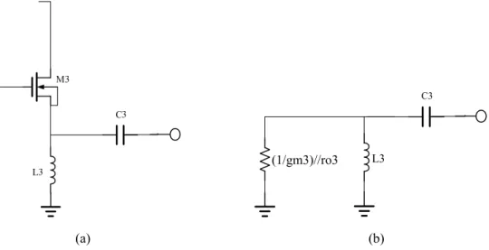
3.3.3 Output Matching Circuit and Analysis ... 39
3.3.4 Forward Body Biasing Technique ... 41
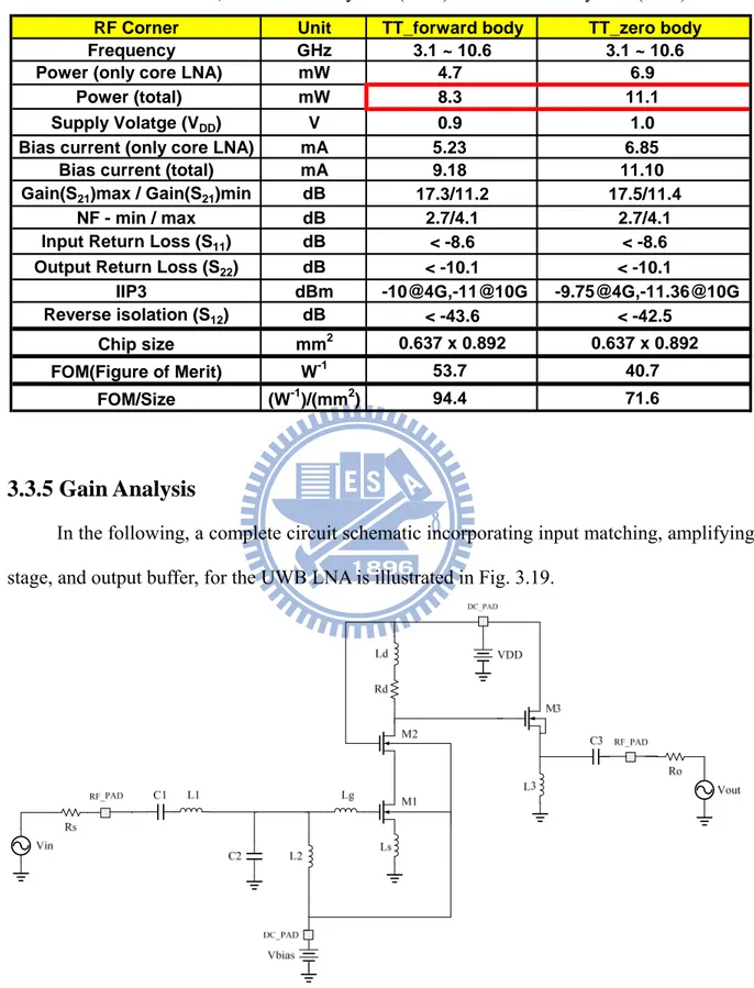
3.3.5 Gain Analysis ... 44
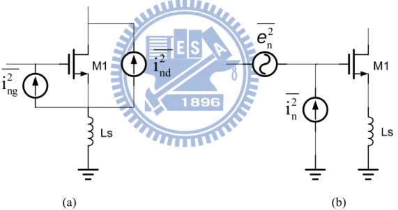
3.3.6 Noise Analysis [5] ... 45
viii
3.4.1 Model for Circuit Simulation ... 50
3.4.2 RF Circuit Simulation for UWB LNA Design ... 51
3.5 Measurement ... 64
3.5.1 Measurement Considerations ... 64
3.5.2 Measurement Results and Discussion ... 66
Chapter 4 Sub-0.2mW Ultra-low Power LNA Design using Forward Body
Biasing Technique ... 74
4.1 Introduction ... 74
4.2 Circuit Architectures for ULP LNA ... 75
4.3 LNA Circuit Analysis ... 76
4.3.1 Gain Analysis ... 77
4.3.2 Noise Analysis [4] ... 78
4.4 Chip Circuit Design and Simulation ... 81
4.4.1 Models for LNA Circuit Simulation ... 82
4.4.2 ULP LNA Simulation Results ... 82
4.5 Measurement ... 94
4.5.1 Measurement Considerations ... 94
4.5.2 Measurement Results and Discussion ... 97
Chapter 5 Conclusion and Future Work ... 106
5.1 Conclusion ... 106
5.2 Future Work ... 107
References ... 109
ix
Figure Captions
Chapter 1
Fig. 1. 1 Wireless Body Area Network of Intelligent Sensors for Patient Monitoring [2] ... 3
Chapter 2
Fig. 2. 1 Traditional transistor-amplifier of input matching ... 5Fig. 2. 2 Resistive termination matching technique ... 6
Fig. 2. 3 Inductive source degeneration matching technique ... 8
Fig. 2. 4 Equivalent circuit of inductive source degeneration matching ... 8
Fig. 2. 5 Shunt-series resistor feedback matching technique ... 9
Fig. 2. 6 Common gate input matching technique ... 10
Fig. 2. 7 The frequency response of a fourth-order Chebyshev low-pass filter with ε = .... 14 1 Fig. 2. 8 Definition of the 1-dB compression point ... 17
Fig. 2. 9 Intermodulation in a nonlinear system ... 19
Fig. 2. 10 (a) The linear gain and the nonlinear component (b) The IIP3 and OIP3 ... 20
Fig. 2. 11 Noisy two-port driven by noisy source ... 22
Fig. 2. 12 Equivalent circuit for two-port noise model ... 22
Fig. 2. 13 Drain current noise model ... 25
Fig. 2. 14 Gate noise circuit model ... 26
Fig. 2. 15 MOSFET noise model ... 27
Fig. 2. 16 Cross-sectional view of the DTMOS device with deep N-well structure ... 28
Chapter 3
Fig. 3. 1 Circuit architecture of the UWB LNA ... 30x
Fig. 3. 2 The circuit schematics of input matching network for UWB LNA ... 31
Fig. 3. 3 Series LC resonance circuit ... 32
Fig. 3. 4 (a) Load ZL (b) The impedance modes of load ZL under varying frequencies, drawn ... 32
Fig. 3. 5 Add a series LC resonance circuit to the load ZL ... 33
Fig. 3. 6 Effect of adding a series LC resonance circuit to the load in the Z-Smith chart ... 33
Fig. 3. 7 Parallel LC resonance circuit ... 33
Fig. 3. 8 (a) Load impedance ZL (b) The impedance modes of load ZL under varying ... 34
Fig. 3. 9 (a) Load admittance YL (b) The admittance modes of load YL under varying ... 34
Fig. 3. 10 Add a parallel LC resonance circuit to the load ... 35
Fig. 3. 11 Effect of adding a parallel LC resonance circuit to the load in the Y-Smith chart ... 35
Fig. 3. 12 An input matching circuit with three-section LC networks for ultra-wide band input ... 36
Fig. 3. 13 The input matching network effect on S11 (a) original nMOSFET without external LC network (b) adding the first section of LC network : Lg and Cgs (c) adding the second section of LC network : L2 and C2 (d) adding the third section of LC network :L1 and C1 ... 37
Fig. 3. 14 (a) Inductive-peaking configuration (b) Small-signal equivalent circuit ... 37
Fig. 3. 15 The output inductance Ld effect on UWB LNA performance from ADS simulation ... 39
Fig. 3. 16 The output matching circuit for UWB LNA (a) the circuit schematic of a Source-follower buffer (b) the Small-signal equivalent circuit for the source-follower ... 40
Fig. 3. 17 Simulated IDS –VDS characteristics for stacked transistors structure (M1 and M2), 42 Fig. 3. 18 UWB LNA performance : power gain (S21), lower noise (NF), input return loss ... 43
xi
Fig. 3. 19 A complete circuit schematic of the UWB LNA ... 44
Fig. 3. 20 Noise model for the amplifying transistor M1. (a) noise sources from drain and gate ... 46
Fig. 3. 21 Contour plots of the average NF [5] ... 49
Fig. 3. 22 Circuit schematic of the UWB LNA with three core circuit blocks in which the .... 52
Fig. 3. 23 Chip layout of the UWB LNA ... 52
Fig. 3. 24 Pre-layout simulation for power gain (S21), input return loss (S11), output return 53 Fig. 3. 25 Pre-layout simulation for reverse isolation (S12) VDD=0.9V, VG=0.4V, ... 53
Fig. 3. 26 Pre-layout simulation for noise figure (NF). VDD=0.9V, VG=0.4V, frequency=2~11 ... 54
Fig. 3. 27 Pre-layout simulation for stability. VDD=0.9V, VG=0.4V, frequency=2~11 GHz... 54
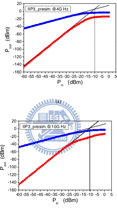
Fig. 3. 28 Pre-layout simulation for third-order intercept point (IIP3) (a) 4GHz : IIP3... 55
Fig. 3. 29 Pre-layout simulation for power gain (S21), under typical (TT) and corner ... 56
Fig. 3. 30 Pre-layout simulation for input return loss (S11), under typical (TT) and corner ... 56
Fig. 3. 31 Pre-layout simulation for output return loss (S22), under typical (TT) and corner 57 Fig. 3. 32 Pre-layout simulation for reverse isolation (S12), under typical (TT) and corner .... 57
Fig. 3. 33 Pre-layout simulation for noise figure (NF), under typical (TT) and corner ... 58
Fig. 3. 34 Comparison between pre-layout and post-layout simulation results for the power . 59 Fig. 3. 35 Comparison between pre-layout and post-layout simulation results for the input ... 59
Fig. 3. 36 Comparison between pre-layout and post-layout simulation results for the output . 60 Fig. 3. 37 Comparison between pre-layout and post-layout simulation results for the reverse 60 Fig. 3. 38 Comparison between pre-layout and post-layout simulation results for noise figure ... 61
Fig. 3. 39 Comparison between pre-layout and post-layout simulation results for stability. ... 61 Fig. 3. 40 Post-layout simulation for third-order intercept point (IIP3) (a) 4GHz : IIP3 =
xii
-11dBm (b) 10GHz IIP3= -10dBm. Two-tone test with tone spacing of 1MHz. ... 62 Fig. 3. 41 On-wafer measurement setup for UWB LNA chip test and characterization ... 64 Fig. 3. 42 Measurement setups for (a) S-parameter & IIP3 & P1dB (b) noise figure ... 65 Fig. 3. 43 UWB LNA chip measured results and comparison with post-layout simulation for
... 69 Fig. 3. 44 UWB LNA chip measured third-order intercept point (IIP3) (a) IIP3 =12dBm at .. 70
Chapter 4
Fig. 4. 1 Circuit architecture of the proposed ultra-low power (ULP) LNA ... 75 Fig. 4. 2 The circuit schematic of ULP LNA... 77 Fig. 4. 3 Small signal equivalent circuit analysis for the ULP LNA ... 77 Fig. 4. 4 (a) a simple cascade structure used as a common source input stage of LNA (b) a
small signal equivalent circuit for the noise model of input stage in LNA ... 79 Fig. 4. 5 Circuit schematic of the ULP LNA with three core circuit blocks in which the active
and passive devices dimensions are provided ... 84 Fig. 4. 6 Chip layout of the designed ULP LNA ... 85 Fig. 4. 7 Pre-layout simulation for ULP LNA (a) power gain (S21), input return loss (S11), output return loss (S22), reverse isolation (S22) (b) noise figure (NF) (c) stability (d)
third-order intercept point (IIP3), two tones space=10MHz, center frequency =1.4GHz. VDD=0.18V, VG=0.45V, VG2=0.8V, VB1=0.4V, VB2=0. ... 87 Fig. 4. 8 Comparison between pre-layout and post-layout simulation results for the ULP LAN (a) power gain(S21) (b) input return loss (S11) (c)output return loss (S22) (d) reverse
isolation (S21) (e) noise figure (NF) (f) stability (g) third-order intercept point (IIP3). VDD=0.18V, VG=0.45V, VG2=0.8V, VB1=0.4V, VB2=0. ... 91 Fig. 4. 9 On-wafer measurement of LNA test diagram ... 95
xiii
Fig. 4. 10 Measurement setups for (a) S-parameter & IIP3 & P1dB (b) noise figure ... 96 Fig. 4. 11 ULP LNA chip measured results for (a) power gain (S21) and reverse isolation (S12) (b) input return loss (S11) and output return loss (S22) (c) noise figure. VDD=0.18V,
VG=0.45V, VG2=0.8V, VB1=0.4V, and VB2=0. ... 100 Fig. 4. 12 The comparison between measurement and ADS simulation by using measured
inductor S-parameters, rather than inductor model (a) power gain (S21) and reverse isolation (S21) (b) input return loss (S11), output return loss (S22), (c) noise figure
(NF). VDD=0.18V, VG=0.45V, VG2=0.8V, VB1=0.4V, and VB2=0. ... 103 Fig. 4. 13 ULP LNA chip measured under raised VDD to 0.5V (a) power gain (S21) and reverse
isolation (S12), input return loss (S11) and output return loss (S22) (b) noise figure.
xiv
Table Captions
Chapter 2
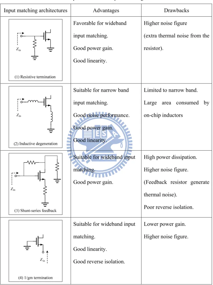
Table 2. 1 Comparison of LNA Input matching architectures ... 12
Chapter 3
Table 3. 1 UWB LNA performance and supply voltages VDD comparison from ADS ... 44 Table 3. 2 Pre-layout simulation results, under typical and corner conditions ... 58 Table 3. 3 Post-layout simulation results, under typical and corner conditions ... 63 Table 3. 4 Comparison of pre-layout and post-layout simulation results (typical condition) .. 63 Table 3. 5 UWB LNA chip measured performance and comparison with post-layout ... 71 Table 3. 6 UWB LNA Performance Benchmark ... 72
Chapter 4
Table 4. 1 Pre-layout simulation for ULP LNA under fixed biases condition for typical (TT) and corner cases (FF, SS). VDD=0.18V, VG=0.45V, VG2=0.8V. VB1=0.4V, and
VB2=0V. ... 91 Table 4. 2 Post-layout simulation for ULP LNA under fixed biases condition for typical (TT)
and corner cases (FF, SS). VDD=0.18V, VG=0.45V, VG2=0.8V. VB1=0.4V, and VB2=0V. ... 92 Table 4. 3 Pre-layout simulation for ULP LNA under tunable biases condition for typical .... 93 Table 4. 4 Post-layout simulation for ULP LNA under tunable biases condition for typical (TT)
and corner cases (FF, SS). ... 94 Table 4. 5 Spiral inductor characteristics measured from the test devices on a single chip with
xv
Table 4. 6 Simulated and measured performance for 1.4GHz LNA under varying VDD and VG
... 104 Table 4. 7 ULP LNA Performance Benchmark ... 105
1
Chapter 1
Introduction
1.1 Background and Motivation
The design of low-power wireless transceivers has gained substantial significance due to the explosion of wireless applications such as personal area networks and wireless sensor
networks. These applications demand small, low-cost, and low-power wireless transceivers, which require a high level of integration with a minimal amount of off-chip components. The
first active block to amplify the received signal from the antenna is the low-noise amplifier (LNA). The specifications of a LNA influence significantly the performances of the whole
receiver. The LNA needs to amplify the signal without adding an inappropriately large noise and distortion while consuming minimal power. How to provide enough gain in a LNA
suitable for a specific wireless communication system without consuming too much power is the main object of this thesis. The important design goal of portable wireless system is low
power consumption for long battery life. In the thesis, two LNAs intended for 3.1~10.6 GHz ultra-wideband (UWB) LNA and 1.4 GHz ultra-lower power LNA are designed and
fabricated.
Regarding the applications of UWB LNAs, the targeted UWB system is an emerging
high-speed and low-power wireless communication domain approved by Federal Communication Commission (FCC) in 2002 for commercial applications in the frequency
range from 3.1 to 10.6 GHz [1]. UWB performs excellently for short-range and high-speed uses, such as automotive collision-detection systems, through-wall imaging systems, and
high-speed indoor networking, and plays an important role in wireless personal area network (WPAN) applications. This technology will be potentially a necessity in our daily life, from
2
wireless USB to wireless connection between DVD player and TV, and the foreseeable huge
market attracts interest of various joint ventures in industries.
As for the ultra-low power LNAs, wireless body area network (WBAN) is identified as
one of the applications of major interest . Wearable health monitoring systems integrated into a telemedicine system can facilitate a novel information technology that is able to support
early detection of abnormal conditions and prevention of its serious consequences. Many patients can benefit from continuous monitoring as part of a diagnostic procedure, optimal
maintenance of a chronic condition or during supervised recovery from an acute event or surgical procedure. Fig. 1.1 shows a generalized overview of multi-tier system architecture [2].
To be unobtrusive, the sensors must be lightweight with small form factor. The size and weight of sensors is predominantly determined by the size and weight of batteries.
Requirements for extended battery life directly oppose the requirement for small form factor and low weight. This implies that sensors have to be extremely power efficient, as frequent
battery changes for multiple WBAN sensors would likely hamper users' acceptance and increase the cost. In addition, low power consumption is very important as we move toward
future generations of implantable sensors that would ideally be self-powered, using energy extracted from the environment.
In this thesis, forward body bias (FBB) scheme was implemented in the LNAs for realizing a substantial VDD scaling to subthreshold region for ultra-low power and maintain
sufficiently good RF performance. Note that 4-terminal (4T) multi-finger MOSFET is the fundamental device structure in which the source and body are separated in two individual
pads to enable non-zero body biases, such as forward or reverse body biases (FBB and RBB). This approach is new and quite different from conventional RF CMOS circuit design, which
is based on 3-terminal (3T) MOSFET with body and source tied together and body bias fixed at zero (ZBB for zero body bias). Besides the change of unit device (MOSFET) layout from
3
3T to 4T, the device model has been adapted and enhanced to improve the accuracy under
various body biases, such as ZBB, FBB, and RBB.
Fig. 1. 1 Wireless Body Area Network of Intelligent Sensors for Patient Monitoring [2]
1.2 Thesis Organization
This thesis presents the work on the design and implementation of ultra-low power
LNAs for receiver front-end circuits. The main objective of this thesis is to develop ultra-low power LNA design methods and certify the proposed topologies using RF CMOS processes.
The contents consist of two major topics, such as “low-power UWB LNA design for 3.1~10.6 GHz wireless receivers” and “sub-0.2mW ultra-low power LNA for wireless body area
network (WBAN) sensors.
In Chapter 2, we will introduce the basic concepts of LNAs design. Some conventional
LNA input matching architecture will be discussed, and MOSFET noise model and the theoretical background will be addressed. Furthermore, dynamic threshold voltage CMOS
technique (by using body biases) is also covered in this chapter.
4
3.1~10.6 GHz UWB applications. We will discuss the circuit topology, the method for
wideband input/output matching, and for the optimization of gain as well as noise. The test chip of LNA was fabricated by TSMC 0.13μm 1P8M CMOS Mixed Signal RF General Purpose Standard Process. The Si data measured from the test chip will be analyzed and compared with what predicted by simulation.
In Chapter 4, a narrow band LNA intended for application in 1.4 GHz WBAN is introduced. The details of circuit design and analysis method will be presented. This ultra-low
power LNA chip was fabricated by UMC 90nm low leakage (logic and mixed-Mode 1P9M low-k) process. The measured results will be compared with the predicted performance from
ADS simulation to verify the proposed circuit topology for ultra-low power, the root causes responsible for deviation from simulation, and the improvement solutions. In Chapter 5,
5
Chapter 2
Basic Concepts of Low Noise Amplifier Design
2.1 Conventional LNA Input Matching Architecture
Low noise amplifier is the first stage in the receiver front-end circuits and is used to
amplify the received weak RF signal with the minimum noise figure. As it is well recognized that impedance matching is the fundamental requirement in LNA designs for achieving the target performance of both gain and noise. There are four basic 50-Ω input matching architectures that have been explored in the traditional transistor-amplifier shown in Fig. 2.1.
In this section, we will have a review and discussion on the mentioned matching circuit architectures that can be used in LNA design [3, 4].
Fig. 2. 1 Traditional transistor-amplifier of input matching
2.1.1 Resistive Termination Architecture [3]
Resistive termination architecture is the most straightforward approach to providing a reasonably broadband 50-Ω termination. It is simply to put a 50-Ω resistor (R1) across the input terminals of the LNA as shown in Fig. 2.2.
The bandwidth of this matching technique is determined by the input capacitance Cgs of the transistor M1 and can be very high. Unfortunately, the resistor R1 adds thermal noise of
6
its own and so attenuates the signal (by a factor of 2) ahead of the transistor. The combination
of these two effects generally produces unacceptably high noise figures. More formally, it is straightforward to establish the lower bound on the noise figure of this circuit, given by (2-1)
[3]: 4 1 2 m NF g R γ α ≥ + ⋅ (2-1) where 0 m d g g
α and γ is the coefficient of channel thermal noise, and Rs =R1= . For R
long-channel devices, 2 3
γ = and α= . This bound applies only in the low-frequency limit 1 and ignores gate current noise altogether. Naturally, the noise figure is worse at higher
frequencies and when gate noise is taken into account. Hence, the resistor termination technique is not practical in most application.
Fig. 2. 2 Resistive termination matching technique
2.1.2 Inductive Source Degeneration Architecture [3]
The inductive source degeneration architecture shown in Fig. 2.3 is popular with input
matching technique of LNA. [4-18]. An important advantage of this method is that one then has control over the value of the real part of the impedance through choice of inductance, as is
clear from computing the input resistance through a circuit analysis on the inductive source degeneration architecture in Fig. 2.3 and the resulted equivalent circuit in Fig. 2.4. This
7
method does not introduce additional noise (as in the case of using a shunt input resistor) and
doesn’t restrict the value of gm (as in the case of the common-gate configuration).
To simplify the analysis, consider a device model that includes only a transconductance
and a gate-source capacitance Cgs. The impedance looking through the gate inductor can be written as: 1 ( ) ( ) in in g in m gs s gs V i j L i g V j L j C ω ω ω = ⋅ + + + ⋅ 1 [ ( ) ] in m s in g s in gs gs V g L Z j L L i C ω ωC ⇒ = = + + − (2-2) From (2-2), in order to achieve an input impedance matching, the following condition must be satisfied: m s s T s gs g L R L C ω = = (2-3) where m T gs g C
ω = is the transit frequency of the transistor M1. Once Ls is chosen based on
gain, linearity and input matching requirements, Lg can then be chosen such that Lg, Ls
and Cgs resonate at a specified frequency ω0 in (2-4). In other words, Lg is determined
according to the following condition:
0 0 1 ( g s) gs L L C ω ω + = 0 1 ( ) gs g s C L L ω ⇒ = + (2-4) At the resonance frequency where the imaginary part of impedance, i.e. the reactance
contributed from the inductors (L ands Lg) and capacitor Cgs are canceled out, the input
impedance is left with just the first term in (2-2), i.e. the resistance representing the real part of impedance.
8
Fig. 2. 3 Inductive source degeneration matching technique
T
L
sω
Fig. 2. 4 Equivalent circuit of inductive source degeneration matching
Note that the form of (2-2) clearly shows that the input impedance is purely resistive at only one frequency (at resonance), however, so this method can provide only a narrowband
impedance matching.
2.1.3 Shunt-Series Resistor Feedback Architecture [3]
The shunt-series resistor feedback architecture as shown in Fig. 2.5 can provide good wideband matching and flat gain, but tends to suffer from poor noise figure (NF) and large
power dissipation. [11, 19-23]
The impedance Zin can be written as RFM. The resistor
1 F FM v R R A =
− represents the Miller equivalent input resistance of RF, where Av is the open-loop voltage gain (Av ≈g Rm1 L). We
9
2.5 suffers from fewer problem than the architecture as shown in Fig. 2.2, yet the resistive
feedback network continues to generate thermal noise of its own and also fails to present to the transistor an impedance that equals Zopt at all frequencies. As a consequence, the overall
amplifier’s noise figure, while usually much better than that of Fig. 2.2.
In the resistive shunt-feedback amplifier, input resistance is determined by the feedback
resistance (RF) divided by the loop-gain of the feedback amplifier. Therefore, the feedback resistor tends to be a few hundred ohms in order to match the low signal source resistance of typically 50-Ω. This inappropriately large resistance generally leads to significant NF degradation. Furthermore, even with a moderate amount of voltage gain, the amplifier
requires a rather large amount of current, especially in the CMOS, due to its strong dependence on the voltage gain from the transconductance of the amplifying transistor M1.
[15] As a consequence, it will consume higher power dissipation and require good quality on-chip resistors for achieving a precise feedback resistance.
Fig. 2. 5 Shunt-series resistor feedback matching technique
2.1.4 Common-Gate Input Architecture (1/gm termination) [3]
The last input matching method for realizing resistive input impedance is to use a
10
source terminal is 1/gm, a proper selection of device size and bias current can provide the desired 50-Ω resistance. Using the common-gate input architecture, the minimal NF which can be achieved at low frequencies and neglecting gate current noise is NF 1 γ 2.2dB
α ≈ + ≥ where 0 m d g g
α and γ is the coefficient of channel thermal noise. Note that for long channel devices, NF=2.2 dB corresponding to α = 1 and γ = 2/3. As for short channel devices ( 1, 2
3
α ≤ γ ≥ ), NF perhaps as high as 4.8 dB ( γ 2
α = ). The noise figure will become significantly worse at higher frequencies and when gate current noise is taken into account.
Fig. 2. 6 Common gate input matching technique
As compared to the conventionally used common-source topology, the common-gate input architecture is an efficient way to achieve a broadband matching with small chip area.
Because it doesn’t need many inductors to achieve wideband input matching. However, it can’t provide sufficient gain and lower noise figure with low power consumption [24].
2.1.5 LNA design and Comparison of Input Matching Architecture
For LNA design, the trade-offs between the gain, noise, and power consumption are
critical factors to be considered for the selection of circuit topologies, impedance matching methods, and details to the active and passive devices design. In the following, the major
11
requirements and trade-offs are described, tentatively as a design guideline.
1) Low power dissipation :
In general, low power RF circuit design is challenging, due to trade-off between gain,
linearity, and noise, etc. For a broadband LNA design, the power dissipation becomes even worse and makes low power design more difficult in the broadband circuits.
2) Input and Output matching (return loss)
In wireless receiver, the components placed in front of LNA are usually filter and antenna with the characteristic impedance 50-Ω, so input impedance matching of LNA must realize a match to 50-Ω. Unfortunately, the architecture for an input impedance matching is always different from that for an optimum noise matching.
3) High power gain
For LNA design, power gain is one of the most important performance parameters to be considered. Power gain should be sufficiently high to amplify the small RF signal from
the receiver and then reduce the noise generated from the following stages. However, the larger power gain will generally degrade the linearity in LNAs.
4) Low Noise Figure (NF):
As it is well known that LNA acting as the amplifier in a receiver system, the noise
generated from itself dominates the noise from all other components following the LNA. Thus, minimizing noise figure (NF) becomes the most important target in LNA design. As
a matter of fact, the optimization of NF is sometime traded off with power gain and power dissipation.
12
Table 2. 1 Comparison of LNA Input matching architectures
Input matching architectures Advantages Drawbacks
Favorable for wideband input matching.
Good power gain. Good linearity.
Higher noise figure
(extra thermal noise from the
resistor).
Suitable for narrow band
input matching.
Good noise performance.
Good power gain. Good linearity.
Limited to narrow band.
Large area consumed by on-chip inductors
Suitable for wideband input
matching.
Good power gain.
High power dissipation.
Higher noise figure.
(Feedback resistor generate
thermal noise).
Poor reverse isolation.
Suitable for wideband input matching.
Good linearity.
Good reverse isolation.
Lower power gain. Higher noise figure.
13
2.2 C
hebyshev Filter [25, 26]
Chebyshev filters are analog or digital filters having a steeper roll-off and more passband
ripple or stopband ripple than Butterworth filters. Chebyshev filters have the property that they minimize the error between the idealized filter characteristic and the actual over the
range of the filter, but with ripples in the passband. This type of filter is named in honor of Pafnuty Chebyshev because their mathematical characteristics are derived from Chebyshev
polynomials.
Because of the passband ripple inherent in Chebyshev filters, filters which have a
smoother response in the passband but a more irregular response in the stopband are preferred for some applications.
2.2.1 Theory of Chebyshev Filter [25, 26]
The gain (or amplitude) response as a function of angular frequency ω of the nth order
low pass filter is
2 2 0 1 ( ) ( ) 1 ( ) n n n G H j T ω ω ω ε ω = = + (2-5)
where ε is the ripple factor, ω0 is the cutoff frequency and Tn( ) is a Chebyshev polynomial of the nth order.
The passband exhibits equiripple behavior, with the ripple determined by the ripple factor ε. In the passband, the Chebyshev polynomial alternates between 0 and 1 so the filter gain will alternate between maxima at G= and minima at 1
2 1 1 G ε = + . At the cutoff frequency ω0 the gain again has the value
2
1
1+ε but continues to drop into the stop band as the frequency increases. This behavior is shown in the diagram on the Fig. 2.7.
14
Fig. 2. 7 The frequency response of a fourth-order Chebyshev low-pass filter with ε = 1 The order of a Chebyshev filter is equal to the number of reactive components (for example, inductors) needed to realize the filter using analog electronics.
The ripple is often given in dB:
Ripple in dB =
2
1 20log
1+ε (2-6) so that a ripple amplitude of 3 dB results from ε = . 1
a. Poles and zeroes
For simplicity, assume that the cutoff frequency is equal to unity. The poles (ωpm) of the
gain of the Chebyshev filter will be the zeroes of the denominator of the gain. Using the complex frequency s:
2 2
1+ε Tn (−js) 0= (2-7) Defining − =js cos( )θ and using the trigonometric definition of the Chebyshev polynomials yields: 2 2 2 2 1+ε Tn (cos( )) 1θ = +ε cos ( ) 0nθ = (2-8) Solving for θ 1 arccos( j) m n n π θ ε ± = + (2-9) where the multiple values of the arc cosine function are made explicit using the integer index
15 m. The poles of the Chebyshev gain function are then:
1
cos( ) cos( arccos( ) ) pm j m s j j n n π θ ε ± = = + (2-10) Using the properties of the trigonometric and hyperbolic functions, this may be written in explicitly complex form:
1 1 1 1
sinh( ar sinh( ))sin( ) cosh( sinh( )) cos( )
pm m m s j ar n ε θ n ε θ ± = ± + (2-11) where m = 1, 2,..., n and 2 1 2 m m n π θ = − .
This may be viewed as an equation parametric in θn and it demonstrates that the poles lie on
an ellipse in s-space centered at s = 0 with a real semi-axis of length
1 sinh( ) sinh( ) ar n ε and an
imaginary semi-axis of length of
1 sinh( ) cosh( ) ar n ε .
2.2.2 Applications of Chebyshev Filter [27]
Filters are signal-processing circuits used to modify the frequency spectrum of an
electrical signal. They may be used to amplify, attenuate, or reject a certain range of frequencies of their input signals. Filters are pervasive in integrated circuits because of their
vast number of applications. Some applications include noise reduction in communication systems, band-limiting of signals before sampling them, conversion of sampled signals into
continuous-time signals, signal demodulation, improving the sound quality of audio system components such as loudspeakers and receivers, and many others.
The Chebyshev response is a mathematical strategy for achieving a faster roll-off by allowing ripple in the frequency response. Analog and digital filters that use this approach are
called Chebyshev filters. For instance, analog Chebyshev filters were used for analog-to-digital and digital-to-analog conversion.
16
The Chebyshev gives a much steeper roll-off, but passband ripple makes it unsuitable for
audio systems. It is superior for applications in which the passband includes only one frequency of interest (e.g., the derivation of a sine wave from a square wave, by filtering out
the harmonics).
2.3 linearity
[28]
Linearity is one of the key requirements in LNA design to maintain linear operation in
the presence of a large interfering signal and when the input is driven by a large signal. Any nonlinear transfer function can be mathematically written as a series expansion of power-law
terms unless the system contains memory. The input Vi and output Vo of a two-port
network can be related by a power series. For simplicity, we make an approximation to the third order term:
2 3
1 2 3
o i i i
V =αV +α V +αV (2-12)
where α1,α2,α3 are constants.
2.3.1 Harmonic Distortion [28]
If a sinusoidal waveform is applied to a nonlinear system, the output generally exhibits
frequency dependent components that are integer multiples of the input frequency. In (2-12),
setting V ti( )=Acos( )ωt , then
2 2 3 3 1 2 3 3 3 2 2 3 3 2 2 1
( ) cos( ) cos( ) cos( ) (2-13.1) 3
( ) cos( ) cos(2 ) cos(3 ) (2-13.2)
2 4 2 4 α ω α ω α ω α α α α ω α ω ω = + + = + + + + o V t A t A t A t A A A A A t t t
In (2-13.1), the term with the input frequency ω is called the “fundamental” and the higher-order terms the “harmonics”. The first term in (2-13.1) is the linear term and is the
ideal output if the two-port network is completely linear. Other terms in (2-13.1) are responsible for nonlinearities, and they cause a DC shift as well as distortion at frequencies
17
2ω , 3ω , and higher harmonics derived in (2-13.2), which result in either gain compression or gain expansion. It can be observed from (2-13.2) that distortion is present in any signal level.
2.3.2 1-dB Compression Point (P1dB) [28]
In most circuits of interest, the output is a “compressive” or “saturating” function of the
input; that is, the gain approaches zero for sufficiently high input levels. In (2-13) this occurs
if α3 < . Written as 0 3 3 1 3 4 A A α
α + , α1A represents the fundamental amplitude and the gain
is therefore a decreasing function of the third-order harmonic proportional to
α
3A3. In RF circuits, this effect is quantified by the “1-dB compression point”, defined as the input signallevel that causes the small-signal gain to drop by 1 dB. As shown in Fig. 2.8, which is plotted on a log-log scale as a function of the input level, the output level falls below its ideal value
by 1 dB at the 1-dB compression point [28].
Fig. 2. 8 Definition of the 1-dB compression point
To calculate the 1-dB compression point, we can write from (2-13.3)
2 1 3 1 1 3 20log 20log 1 4 A dB dB α + α − = α − (2-14) That is, 1 1 3 0.145 dB A α α − = (2-15)
18
2.3.3 Intermodulation [28]
Harmonic distortion that was introduced previously is the result of nonlinearities due to a single sinusoidal input. When two signals with different frequencies are applied to a nonlinear
system, the output in general exhibits some components that are not harmonics of the input frequencies. Called intermodulation (IM), this phenomenon arises from “mixing”
(multiplication) of the two signals when their sum is raised to a power greater than unity. To investigate the effects of both harmonic distortion and intermodulation, we assume that the input signal is composed of two different frequencies ω and 1 ω given in (2-16) 2
1 1 2 2
( ) cos( ) cos( )
i
V t =A ωt +A ωt (2-16)
(2-16) can be substituted into (2-12). Thus, the output can be expressed as
2
1 1 1 2 2 2 1 1 2 2
3
3 1 1 2 2
( ) [ cos( ) cos( )] [ cos( ) cos( )] [ cos( ) cos( )] o V t A t A t A t A t A t A t α ω ω α ω ω α ω ω = + + + + + (2-17)
Expanding the right-hand side and discarding the dc terms and harmonics, we obtain intermodulation products expressed in (2-18) and (2-19) for the second order and (2-20) for
the third order IM products, namely IM2 and IM3.
1 2: 2 1 2A A cos[( 1 2) ]t 2 1 2A A cos[( 1 2) ]t ω ω ω α= ± ω ω+ +α ω ω− (2-18) 2 2 3 1 2 3 1 2 1 2 1 2 1 2 3 3 2 : cos[(2 ) ] cos[(2 ) ] 4 4 A A A A t t α α ω ω ω ω ω ω = ± + + − (2-19) 2 2 3 2 1 3 2 1 2 1 2 1 2 1 3 3 2 : cos[(2 ) ] cos[(2 ) ] 4 4 A A A A t t α α ω ω ω ω ω ω = ± + + − (2-20)
and the fundamental components written in (2-21)
3 2 1 2 1 1 3 1 3 1 2 1 3 2 1 2 3 2 3 2 1 2 3 3 , : ( ) cos( ) 4 2 3 3 ( ) cos( ) 4 2 A A A A t A A A A t ω ω ω α α α ω α α α ω = + + + + + (2-21)
Of particular interest are the third-order IM products at 2ω ω1− 2 and 2ω ω2− , illustrated in 1 Fig. 2.9 in which the input RF signals are two-tone with two different frequencies such as
19 1
ω and ω 2
Fig. 2. 9 Intermodulation in a nonlinear system
where it is assumed that A1= A2 = . A
From Fig. 2.9, it is apparent that the third-order intermodulation distortion IM3 signals are
close to the signals of interest F, which makes the filtering out of IM3 signals difficult when recovering the signals of interest. Therefore minimizing intermodulation distortion is a key
objective in many RF circuit design.
2.3.4 Third-Order Intercept Point (IIP3) [28]
From (2-17)~(2-21) and let A1= A2 = , we can drive the expression A
2 2 1 3 1 1 3 2 3 3 3 1 2 3 2 1 9 9 ( ) ( ) cos( ) ( ) cos( ) 4 4 3 3 cos[(2 ) ] cos[(2 ) ] 4 4 o V t A A t A A t A t A t α α ω α α ω α ω ω α ω ω = + + + + − + − +… (2-22)
We note that as the input amplitude A is small to keep 1 9| 3| 2 4
α >> α A , the fundamentals
increase proportional to A , whereas if the input level A increases to the intercept point so
that 1 3 2
9 | | 4
α >> α A is no longer valid, the gain will drop and the third-order IM products in proportion to A3 will take over the fundamentals, as shown in Fig. 2.10(a). Plotted on a
logarithmic scale [Fig. 2.10(b)], the magnitude of the IM products grows at three times the rate at which the main components increase. The third-order intercept point, namely IP3 is
defined to be at the intersection of the two lines. The horizontal coordinate of this point is called the input IP3 (IIP3), and the vertical coordinate is called the output IP3 (OIP3).
20
(a) (b)
Fig. 2. 10 (a) The linear gain and the nonlinear component (b) The IIP3 and OIP3
If 2
1 3
9 4 A
α α , the input level for which the output components at ω1 and ω2 have the
same amplitude as those at those at 2ω ω1− 2 and 2ω ω2− is given by 1
3 1 3 3 3 3 4 IP IP A A α = α (2-23) Thus, the input IP3 is
1 3 3 4 3 IP A α α = (2-24)
2.4 Stability
[29]
One more important consideration for an amplifier design like LNA is the assurance of
stability. For LNAs in the form of a two-port network, the requirement for ensuring stability is that it must not produce an output with oscillatory behavior. The stability of a two-port
network can be determined from the S-parameters, the matching networks, and the terminations. Simpler tests can be used to determine unconditional stability [29]. One of these is the K-△ test, where it can be shown that a device will be unconditionally stable if Rollet’s
condition [30], defined as 2 2 2 11 22 12 21 1 1 2 S S K S S − − + Δ = > (2-25)
21
along with the auxiliary condition that
11 22 12 21 1 S S S S
Δ = − < (2-26) are simultaneously satisfied. These two conditions are necessary and sufficient for unconditional stability.
While the K-△ test of (2-25)~(2-26) is a mathematically rigorous condition for
unconditional stability, it cannot be used to compare the relative stability of two or more
devices since it involves constraints on two separate parameters. However, a new criterion has been proposed [31] that combines the S parameters in a test involving only a single parameter, μ, defined as 2 11 * 22 11 21 12 1 1 S S S S S μ = − > − Δ + (2-27) Thus, if μ >1, the device is unconditionally stable. In addition, it can be said that larger values of μ implies greater stability.
2.5 Noise in Two-Port System
[3]
2.5.1 Noise Factor
Noise factor (F) is defined as the signal-to-noise power ratio at the input to the signal-to-noise power ratio at the output. Considering a network with gain G and noise Na,
noise factor then can be express as (2-28) [3]
/ / @
/ ( ) /[ ( )] @
i i i i i a o
o o i i a i i
S N S N N N N Total noise power output F
S N GS G N N N GN Noise power output due to source only
+ ≡ = = = = + (2-28) Generally we use this measure in the unit of dB, namly noise figure (NF) written in (2-29)
10 log
NF = F (2-29)
22
and given in (2-28). To define it and understand why it is useful, consider a noisy (but linear)
two-port network driven by a source that has an impedance Zs and an equivalent series noise
voltage 2
s
e , illustrated in Fig. 2.11.
If we are concerned only with overall input-output behavior, it is an unnecessary complication to keep track of all of internal noise source. Fortunately, the net effect of all of
those sources can be represented by just one pair of external sources like a noise voltage 2
n e
and a noise current 2
n
i as shown in Fig.2.12. This simplification allows a rapid evaluation of
how the source impedance affects the overall noise performance. As a consequence, we can identify the criteria, which one must satisfy for optimum noise performance.
Fig. 2. 11 Noisy two-port driven by noisy source
Fig. 2. 12 Equivalent circuit for two-port noise model
Carrying out the calculations based on the equivalent circuit of noisy two-port illustrated in Fig.2.12, the noise factor is written as
23 2 2 2 s n s n i a i s e e Z i N N F N e + + + = = (2-30) In order to accommodate the possibility of correlations between en and in, express en as the
sum of two components in (2-31) in which enc, represents the term correlated with in, and enu, the un-correlated term.
n nc nu
e =e +e (2-31)
Since en is correlated with in, it may be treated as proportional to in through a constant namely
ZC whose dimensions are those of impedance:
nc c n
e =Z i (2-32)
Combining (2-30), (2-31), and (2-32), the noise factor becomes
2 2 2 2 2 2 2 ( ) 1 s nu c s n nu c s n s s e e Z Z i e Z Z i F e e + + + + + = = + (2-33) The expression in (2-33) contains three independent noise sources, each of which may be
treated as thermal noise produced by an equivalent resistance or conductance:
2 2 2 , , 4 4 4 nu s n u s n e e i R R G kT f kT f kT f ≡ ≡ ≡ Δ Δ Δ (2-34) Using these equivalences, the expression for noise factor can be written purely in terms of
impedances and admittances:
(
) (
2)
2 2 1 u c s n 1 u c s c s n s s R R R X X G R Z Z G F R R ⎡ ⎤ + + + + + + ⎣ ⎦ = + = + (2-35)where Zc =Rc+ jXcis the correlation impedance and Zs =Rs+ jXsis the source impedance.
2.5.2 Optimum Source Impedance [3]
Once a given two-port’s noise has been characterized with its four noise parameters
24
the noise factor. Taking the first derivative with respect to the source impedance and setting
it equal to zero yields the optimal source reactance Xopt and resistance Ropt in (2-36) and (2-37), respectively s c opt X = −X =X (2-36) 2 u s c opt n R R R R G = + = (2-37) Hence, to minimize the noise factor, the source reactance Xs should be made equal to the inverse of the correlation reactance Xc, while the source resistance Rs should be set equal to
the value in (2-37).
The noise factor corresponding to this optimal condition is the minimum noise factor,
namely Fmin, which is derived by direct substitution of (2-36) and (2-37) into (2-35) and expressed as (2-38):
(
)
2 min 1 2 n opt c 1 2 n u c c n R F G R R G R R G ⎛ ⎞ = + + = + ⎜⎜ + + ⎟⎟ ⎝ ⎠ (2-38) We may also express the noise factor in terms of Fmin and the source impedance:(
) (
2)
2min n s opt s opt s G F F R R X X R ⎡ ⎤ = + ⎢ − + − ⎥ ⎣ ⎦ (2-39)
2.6 Noise Sources in MOSFET
[3]
To develop good CMOS RF circuit design skills, a fundamental understanding of noise
source in a MOSFET is necessary. We will focus on the inherent noise of a MOSFET, which can be categorized into two parts: drain noise source and gate noise source.
2.6.1 Drain Noise Source
For a MOSFET under operation, the conducting channel behaves like a
25
illustrated in Fig.2.13. This noise can be expressed as [3]
2 0 4 nd d i = kT gγ Δf (2-40)
Where gd0 is the drain-source transconductance at VDS=0V. For long channel devices, γ is close to unity in its triode region and decreases to about 2/3 when in saturation
(i.e. 2 1
3 ≤ ≤γ ). In long channel case, gd0 is equal to the gate transconductance gm in saturation region which leads to a familiar result
2 0 8 8 3 3 nd d m i = kTg Δ =f kTg Δf (2-41)
Due to the carrier heating driven by the large electric fields in short channel devices [3] or channel length modulation effect [3], γ may become larger than 2 oreven larger.
2 nd
i
Fig. 2. 13 Drain current noise model
2.6.2 Gate Noise Source
Fig.2.14 presents the gate noise circuit model in which the gate noise can be introduced
from the channel region through the capacitive coupling (Cgs) to the gate terminal, due to the fluctuating potential. Also, noisy gate current may be produced by thermally noisy resistive
gate material, denoted as gate resistance (Rg). This component is defined as extrinsic gate noise, which is distinguished from the intrinsic (induced) gate noise originated from channel
potential fluctuation and coupling through Cgs. As the operation frequency increases, contribution of this noise can’t be neglected. This noise can be expressed as (2-42) [3]
26 2 4 ng g i = kT gδ Δ (2-42) f where gg is given by 2 2 gs g d0 C g = 5g ω (2-43)
Because the channel noise and induced gate noise have a common origin, they do have correlation. The correlation coefficient is usually expressed as c in (2-44)
* 2 2 0.395 ng nd ng nd i i c j i i ≡ ≈ − (2-44) The value of -0.395j is exact for long-channel devices. The correlation can be treated by expressing the gate noise as the sum of the two components, the first of which is fully
correlated with the drain noise, and the second of which is uncorrelated with the drain noise. Hence, the gate noise is re-expressed as
2 2
2 4 (1- ) 4
ng g g
i = kT gδ c Δ +f kT g cδ Δ (2-45) f
where the first term is uncorrelated and the second term is correlated to drain noise.
2
ng
i
g
gC
gsFig. 2. 14 Gate noise circuit model
2.6.3 MOSFET Noise Model
A standard MOSFET noise model can be expressed in Fig. 2.15, where 2
ng
i is the gate
noise source, 2
nd
27 2 ng
i
C
gsg V
m gsr
o 2 ndi
Fig. 2. 15 MOSFET noise model
2.7 Dynamic Threshold Voltage
CMOS
The threshold voltage (Vth) of a MOSFET is expressed as
(
)
0 2 2
th th f bs f
V =V +γ ϕ −V − ϕ (2-46)
where Vth0 is the threshold voltage when Vbs = , 0 γ is the body-effect coefficient, ϕ is f
the bulk Fermi potential. Note that Vbs is the voltage between body and source. Thus,
changing Vbs can modify Vth, which can achieve a dynamic threshold voltage MOSFET
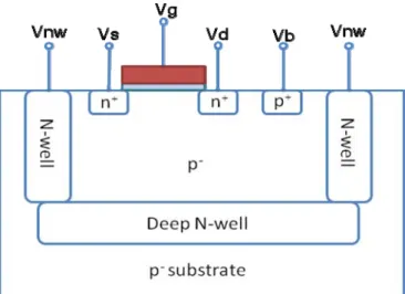
(DTMOS). Threshold voltage is decreased as the external bias Vbs is increased toward the forward direction for the substrate. Usually, the junction between body and source is
zero-biased or reverse-biased. To further improve performance under continuously scaled
supply voltage (VDD), forward body bias (FBB) method becomes attractive for reducing Vth,
according to (2-46). Here, we introduce this concept into low voltage LNA design. To
implement forward body bias scheme in NMOSFET, a deep N-well process is needed as shown in Fig.2.16, which can provide separate body region for each NMOS transistor and
allow the freedom of body biases. In addition, a deep N-well process can reduce noise cross-talk through the substrate. In this thesis, FBB method has been extensively used in
28
29
Chapter 3
Low-Power UWB LNA Design using Forward Body
Biasing Technique for 3.1~10.6 GHz Wireless Receivers
3.1 Introduction
Wideband systems have recently gained much attention due to their capability of high
data rate transmission. The so called ultra-wide band (UWB) technology can pave the way for a wide range of applications, which use the frequency bands in 3.1 ~ 10.6 GHz and can
co-exist with the already licensed spectrum users. To interface with the antenna and pre-select filter in a receiver system, the low-noise amplifier (LNA) input impedance should be close to 50-Ω across the band from 3.1 to 10.6 GHz.
There are several existing solutions for wideband amplifiers in CMOS technology. The
distributed amplifier (DA) is widely used for wideband application due to its intrinsic broadband frequency response going all the way down to dc along with good input and output
impedance matching. Yet, so far, high power consumption and large die area have hampered its widespread applications [32-34]. Recently, the RC feedback topology is widely used for
wideband application. It can provide good wideband matching and flat gain but it can’t provide sufficient gain and lower noise figure with low power consumption [35, 36]. Another
efficient way to achieve a broadband matching is the common-gate input topology [24]. However, the mentioned weaknesses in terms of gain, noise, and power consumption cannot
be solved. For the UWB technology to be widely employed in the hand-held wireless applications, it cannot be avoided that power consumption is one of the main challenges. In
this chapter, we present a UWB LNA with broadband impedance matching, low noise figure (NF), low power consumption, and small chip-area. We focus on the design and
30
implementation of UWB LNA with very low power consumption in a 0.13um CMOS
technology.
3.2 Circuit Architectures
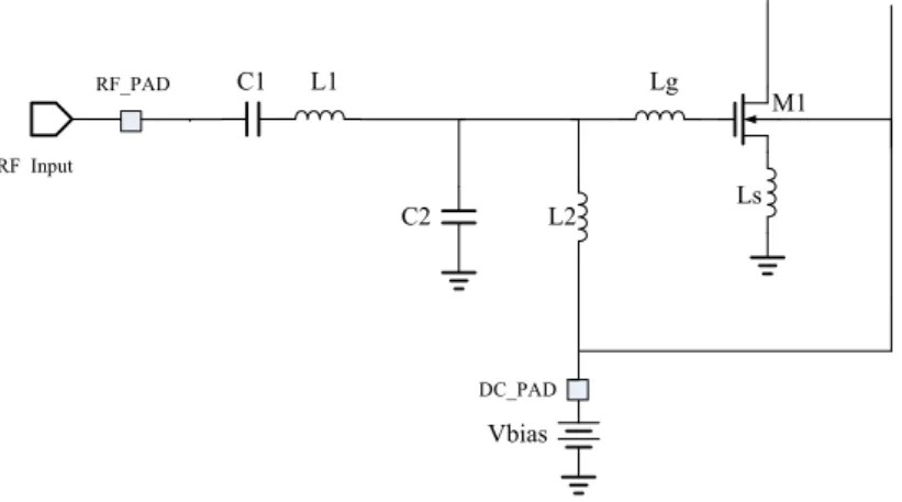
Fig. 3.1 illustrates the circuit architecture of our proposed UWB LNA which is composed of an input matching network, cascode topology, shunt peaking circuit and output
buffer. For a circuit analysis, this UWB LNA can be divided into three blocks – input matching stage, amplifying stage and source-follower buffer stage.
Fig. 3. 1 Circuitarchitecture of the UWB LNA
In the following, the function of each element in the circuit architecture will be
interpreted to explain the UWB LNA design concept. First for the input matching stage, a three-section Chebyshev filter was used, combining the gate-source capacitance (Cgs) of M1
and the source degeneration inductance Ls. This input matching circuit is aimed at a broadband matching from 3.1 to 10.6 GHz.
31
scheme was adopted to reduce the supply voltage and power consumption. The cascade
structure can offer the advantages, such as less Miller effect, better reverse isolation, wider frequency response, and lower noise figure [28, 29]. FBB technique can facilitate low-voltage
UWB LNA design by reducing transistor’s threshold voltage (VT). Shunt peaking method can improve the gain at low frequency and extend the usable bandwidth.
Finally for source-follower buffer stage, an output matching buffer composed of M1, L3, and C3 shown in Fig.3.1 was designed to achieve flat gain over the entire bandwidth and
improve the gain at high frequency. Note that the dimensions of M3, L3 and C3 will determine the high-frequency characteristic of UWB LNA and an appropriate selection of the
layout dimensions is indispensable to achieve a wideband output matching from 3.1 to 10.6 GHz.
3.3 Circuit Topology Analysis
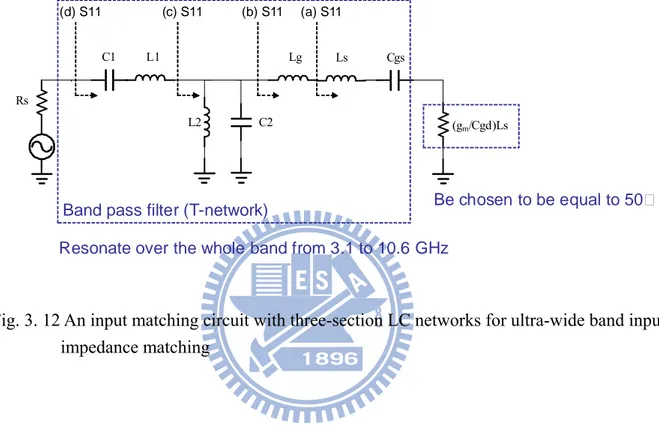
3.3.1 Input Matching Circuit and Analysis [37-39]
Fig. 3.2 illustrates an input impedance matching circuit in the form of multi-section LC networks proposed for UWB LNA in this thesis. The implemented matching network is
built and operates based on the LC resonance matching technique. In the following, the theory and circuit operation principle of this matching network will be described to detail.
RF Input Ls Lg Vbias RF_PAD M1 L2 C2 L1 C1 DC_PAD
32
a. Series LC resonance method:
First, a series LC resonance network is depicted in Fig. 3.3 and the impedance
corresponding to this LC network can be derived as shown in (3-1).
C L
ZS
Fig. 3. 3 Series LC resonance circuit
1 1 ( ) s Z j L j L j C C ω ω ω ω = + = − (3-1) s =0 For Z 0 1 = ω ω = LC
ω0 is the series resonance frequency
for < ω ω0 : Z = jX : capacitive mode reactances −
for > ω ω0 : Z = + jX : inductive mode reactances
Now, set a load Z illustrated in Fig. 3.4 (a) and the impedance of L Z under varying L
frequencies is shown in the Z-Smith chart in Fig. 3.4 (b). It shows that Z is a kind of L
inductive mode impedance at lower frequency ω1 <ω0and becomes a capacitive mode at
higher frequencyω2 >ω0.
(a) (b)
Fig. 3. 4 (a) Load ZL (b) The impedance modes of load ZL under varying frequencies, drawn in the Z-Smith chart
33
Then, we can add a series LC resonance circuit to the load ZL, as shown in Fig. 3.5.
Z
LC
L
Zin
Fig. 3. 5 Add a series LC resonance circuit to the load ZL
The above analysis provide us a guideline to select suitable L and C to generate capacitive
mode impedance (–jX2) at lower frequency and inductive mode impedance(jX1) at higher frequency. In the way, the created series LC network can offer the required impedances to just
cancel out that of load ZL, i.e. the inductive mode jX1 at lower frequency and capacitive mode -jX2 at higher frequency. As a result, the equivalent impedance of the input Zin can approach
the real axis, shown in Fig. 3.6.
Fig. 3. 6 Effect of adding a series LC resonance circuit to the load in the Z-Smith chart
b. Parallel LC resonance method:
Fig. 3.7 illustrates a parallel LC resonance network. The admittance corresponding to this
parallel LC network can be derived as shown in (3-2).
![Fig. 1. 1 Wireless Body Area Network of Intelligent Sensors for Patient Monitoring [2]](https://thumb-ap.123doks.com/thumbv2/9libinfo/8256351.171901/20.892.177.746.192.763/wireless-body-area-network-intelligent-sensors-patient-monitoring.webp)