1236 IEEE ELECTRON DEVICE LETTERS, VOL. 29, NO. 11, NOVEMBER 2008
Impacts of N
2
and NH
3
Plasma Surface Treatments
on High-Performance LTPS-TFT With
High-κ
Gate Dielectric
Ming-Wen Ma, Tien-Sheng Chao, Tsung-Yu Chiang, Woei-Cherng Wu, and Tan-Fu Lei
Abstract—Low-temperature polycrystalline-silicon thin-film transistors (LTPS-TFTs) with high-κ gate dielectrics and plasma surface treatments are demonstrated for the first time. Significant field-effect mobility μFE improvements of ∼86.0%
and 112.5% are observed for LTPS-TFTs with HfO2 gate
dielectric after N2 and NH3 plasma surface treatments,
res-pectively. In addition, the N2and NH3plasma surface treatments
can also reduce surface roughness scattering to enhance the field-effect mobility μFEat high gate bias voltage VG, resulting
in 217.0% and 219.6% improvements in driving current, respectively. As a result, high-performance LTPS-TFT with low threshold voltage VTH∼ 0.33 V, excellent subthreshold
swing S.S. ∼0.156 V/decade, and high field-effect mobility μFE∼ 62.02 cm2/V· s would be suitable for the application of
system-on-panel.
Index Terms—High-κ, low-temperature polycrystalline-silicon thin-film transistors (LTPS-TFTs), NH3plasma, N2plasma.
I. INTRODUCTION
H
IGH-PERFORMANCE low-temperature polycrystalline-silicon thin-film transistors (LTPS-TFTs) with high-κ gate dielectrics have been studied in recent years [1]–[5]. High-κ gate dielectrics can provide higher gate capacitance density with the same physical thickness due to their high dielectric constant. A higher gate capacitance density can attract more carriers with a smaller gate voltage to fill up the traps that exist in the polycrystalline-silicon channel film. Therefore, the LTPS-TFT with high gate capacitance den-sity could significantly reduce the operation voltage without any defect-passivation treatment [1]–[5]. The threshold voltageVTH and the subthreshold swing (S.S.) can be significantly reduced by using high-κ gate dielectrics instead of conven-tional thick SiO2 gate dielectrics [1]–[5]. However, the trap states still exist among the polycrystalline silicon in spite of the employment of high-κ gate dielectrics. The NH3 plasma
Manuscript received July 23, 2008. First published September 16, 2008; current version published October 22, 2008. This work was supported by the National Science Council, Taiwan, under Contract NSC-96-2221-E-009-189. The review of this letter was arranged by Editor A. Nathan.
M.-W. Ma and T.-F. Lei are with the Institute of Electronics, National Chiao Tung University, Hsinchu 300, Taiwan, R.O.C. (e-mail: william.ee94g@nctu. edu.tw; [email protected]).
T.-S. Chao, T.-Y. Chiang, and W.-C. Wu are with the Institute and Depart-ment of Electrophysics, National Chiao Tung University, Hsinchu 300, Taiwan, R.O.C. (e-mail: [email protected]; [email protected]; [email protected]).
Color versions of one or more of the figures in this letter are available online at http://ieeexplore.ieee.org.
Digital Object Identifier 10.1109/LED.2008.2004781
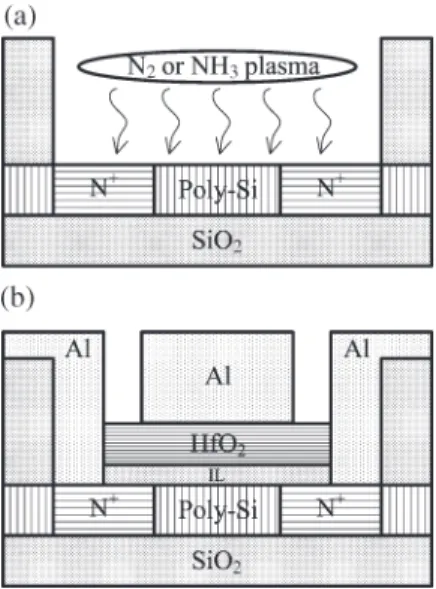
Fig. 1. Cross-sectional view of LTPS-TFT with plasma surface treatment and HfO2gate dielectric.
posttreatment is the most general method to passivate the trap states of the polycrystalline-silicon channel film for conven-tional TFTs [6], [7]. The impacts of NH3plasma treatment on the LTPS-TFT with high-κ gate dielectric have not been re-ported yet.
In this letter, the LTPS-TFT with HfO2 gate dielectric and NH3 plasma surface treatment is demonstrated for the first time. In addition, N2 plasma surface treatment is also used to distinguish the impacts of nitrogen and hydrogen species.
II. EXPERIMENTALPROCEDURE
The fabrication of devices started by depositing a 50-nm undoped amorphous-Si (α-Si) layer at 550◦C in a low-pressure chemical vapor deposition system on Si wafers capped with a 500-nm thermal oxide layer. Then, the 50-nm α-Si layer was recrystallized at 600◦C for 24 h. Then, a 500-nm silicon oxide was deposited by plasma-enhanced chemical vapor deposition at 300 ◦C for device isolation. The device active region was formed by patterning and etching the isolation oxide. The source and drain (S/D) regions in the active device region were implanted with phosphorus at 15 keV and 5× 1015 cm−2. The S/D was activated at 600 ◦C for 24 h. Then, NH3 or N2 plasma surface treatment was performed for 0, 5, and 15 min at 300◦C with a power density of 1.6 mW/cm2in NH3or N2gas, as shown in Fig. 1(a). The flow rate was 100 sccm at pressure
MA et al.: IMPACTS OF N2AND NH3PLASMA SURFACE TREATMENTS ON HIGH-PERFORMANCE LTPS-TFT 1237
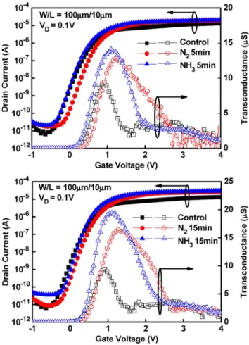
Fig. 2. Transfer characteristics (ID–VG and transconductance Gm) of
LTPS-TFT with HfO2gate dielectric after N2and NH3plasma surface treat-ments for 5 and 15 min, respectively. The solid and hollow symbols represent the IDand Gm, respectively.
of 67 Pa. A 50-nm HfO2 with effective oxide thickness of
∼10.7 nm was deposited by an electron beam evaporation
system at room temperature and pressure of 5× 10⁻⁶ torr without gas flow. An O2 treatment in furnace was applied to improve the HfO2quality at 400◦C for 30 min. The dielectric constant of HfO2 is about 18.2. After the patterning of S/D contact holes, aluminum was deposited by thermal evaporation system as the gate electrode and S/D contact pad. Finally, the TFT devices were completed by the contact pad definition, as shown in Fig. 1(b). Devices with gate length (L) and width (W ) of 10 and 100 μm, respectively, were measured. The threshold voltage VTH is defined as the gate voltage at which the drain current reaches 10 nA× W/L and VD= 0.1 V. The
field-effect mobility μFEis extracted from the maximum transcon-ductance (Gm).
III. RESULTS ANDDISCUSSION
Fig. 2 shows the transfer characteristics (ID–VG and
transconductance Gm) of the LTPS-TFT with HfO2 gate di-electric after N2 and NH3 plasma surface treatments for 5 and 15 min, respectively. The important device parameters of LTPS-TFTs are listed in Table I. The S.S.’s of devices show improvements of 8.6% and 9.6% with N2plasma surface treatment for 5 and 15 min, respectively. Moreover, the μFE’s
of devices also show increases of 43.7% and 86.0% with N2 plasma surface treatment for 5 and 15 min, respectively. It is known that S.S. and μFE are related to the dangling-bond deep trap states and the strain-bond tail trap states of the polycrystalline-silicon channel [8], respectively. The significant increase on μFEindicates that nitrogen has better passivation effect on strain-bond tail trap states than on dangling-bond deep trap states. On the other hand, devices show 9.1% and 21.2% S.S. improvements with NH3plasma surface treatment for 5 and 15 min, respectively. In addition, the 5- and 15-min NH3plasma surface treatments show 51.4% and 112.5% μFE improvements, respectively. It is found that the improvement of S.S. is on the same level by either 5-min N2 or NH3 plasma treatment. This implies that hydrogen from NH3 has less significant contribution to the improvement of S.S. for such a short 5-min treatment. On the contrary, devices with a longer 15-min NH3 plasma treatment exhibit more S.S. im-provement, indicating more passivation effect on the dangling-bond deep trap states due to the contribution of hydrogen. Devices with either 15-min N2or NH3plasma treatment show significant μFEimprovement, indicating that good passivation on strain-bond tail states can be achieved by both plasma treat-ments. Fig. 3 shows the output characteristics (ID–VD) of the
LTPS-TFT with HfO2gate dielectrics after N2and NH3plasma surface treatments for 5 and 15 min, respectively. For 5 min, N2 and NH3 plasma surface treatments show 165.0% and 91.3% driving saturation current ID_satenhancements at VG−VTH= 4 V and VD= 5 V, as shown in Table I and Fig. 3. The 5-min
N2plasma surface treatment shows a smaller μFEimprovement and a higher ID_satenhancement than the 5-min NH3 plasma surface treatment. From Fig. 2, it is noted that the μEFreduction rate after the peak is improved using plasma surface treatment at high VG. This improvement is due to the reduced surface
roughness scattering [9]. The N2 plasma-treated device has more improvement on surface roughness scattering than the NH3plasma-treated device for 5-min treatment time, resulting in a higher driving saturation current ID_satof the N2 plasma-treated device. The surface roughness scattering is improved further, leading to 217.0% and 219.6% improvements in driving saturation current for the 15-min N2and NH3 plasma surface treatments, respectively.
In addition to the performance improvement of the HfO2 LTPS-TFT after plasma surface treatment, the gate capacitance density CGalso decreased due to the growth of interfacial layer
(IL) during the plasma treatment. As shown in Table I, the HfO2 LTPS-TFT after N2 plasma surface treatment has lower CG
than after NH3 plasma surface treatment, suggesting that the thickness of IL grown by N2 plasma is thicker than the one grown by NH3 plasma. The gate leakage current IG of HfO2 LTPS-TFTs after plasma surface treatment at VG− VTH = 2 V and VDS= 0.1 V are also measured and listed in Table I. Much more IGreduction of the N2plasma-treated device is observed to consist with the results of decreased CG. The effective
interface trap states Nit’s and effective grain boundary trap states Ntrap’s of the poly-Si channel film were extracted from S.S. and ID–VG curve [10]–[12]. These values are all listed
in the Table I. The Nit’s of N2 plasma-treated devices show a higher initial improvement due to the growth of IL by N2
1238 IEEE ELECTRON DEVICE LETTERS, VOL. 29, NO. 11, NOVEMBER 2008
TABLE I
IMPORTANTDEVICEPARAMETERS OFLTPS-TFT WITHHfO2GATEDIELECTRICAFTERN2ANDNH3PLASMA
SURFACETREATMENTS FOR5AND15MIN, RESPECTIVELY
Fig. 3. Output characteristics (ID–VD) of LTPS-TFT with HfO2 gate di-electric after N2 and NH3 plasma surface treatments for 5 and 15 min, respectively.
plasma treatment. However, for longer 15-min plasma treat-ment, the effect of NH3plasma on Nitis greater than that of N2 plasma due to hydrogen incorporation. In addition, as shown in Table I, NH3 plasma treatment shows greater passivation effect on grain boundary traps Ntrap’s compared to N2plasma treatment.
High-performance LTPS-TFT with low threshold voltage
VTH ∼ 0.45 V, excellent S.S. ∼ 0.179 V/decade, and high field-effect mobility μFE∼ 54.30 cm2/V· s is obtained by using HfO2gate dielectric and 15-min N2plasma surface treatment. In addition, high-performance LTPS-TFT with low threshold voltage VTH∼ 0.33 V, excellent S.S. ∼ 0.156 V/decade, and high field-effect mobility μFE∼ 62.02 cm2/V· s is also ob-tained by using HfO2gate dielectric and 15-min NH3 plasma surface treatment.
IV. CONCLUSION
In this letter, high-performance LTPS-TFT with HfO2 gate dielectric has been fabricated. In order to enhance the per-formance of the LTPS-TFT with high-κ gate dielectric, two kinds of plasma, N2and NH3, are employed. S.S., field-effect mobility μFE, and driving saturation current are all significantly improved after N2and NH3plasma surface treatments.
ACKNOWLEDGMENT
The authors would like to thank the process support from Na-tional Nano Device Laboratories and the Nano Facility Center, National Chiao Tung University, Hsinchu, Taiwan, R.O.C.
REFERENCES
[1] T.-M. Pan and T.-W. Wu, “High-performance polysilicon TFTs using stacked Pr2O3/oxynitride gate dielectric,” IEEE Electron Device Lett., vol. 29, no. 4, pp. 353–356, Apr. 2008.
[2] C.-W. Chang, C.-K. Deng, J.-J. Huang, H.-R. Chang, and T.-F. Lei, “High-performance poly-Si TFTs with Pr2O3 gate dielectric,” IEEE Electron Device Lett., vol. 29, no. 1, pp. 96–98, Jan. 2008.
[3] M.-J. Yang, C.-H. Chien, Y.-H. Lu, G.-L. Luo, S.-C. Chiu, C.-C. Lou, and T.-Y. Huang, “High-performance and low-temperature-compatible p-channel polycrystalline-silicon TFTs using hafnium-silicate gate di-electric,” IEEE Electron Device Lett., vol. 28, no. 10, pp. 902–904, Oct. 2007.
[4] C.-P. Lin, B.-Y. Tsui, M.-J. Yang, R.-H. Huang, and C. H. Chien, “High-performance poly-silicon TFTs using HfO2gate dielectric,” IEEE Elec-tron Device Lett., vol. 27, no. 5, pp. 360–363, May 2006.
[5] B. F. Hung, K. C. Chiang, C. C. Huang, A. Chin, and S. P. McAlister, “High-performance poly-silicon TFTs incorporating LaAlO3as the gate dielectric,” IEEE Electron Device Lett., vol. 26, no. 6, pp. 384–386, Jun. 2005.
[6] H.-C. Cheng, F.-S. Wang, and C.-Y. Huang, “Effects of NH3plasma pas-sivation on n-channel polycrystalline silicon thin-film transistors,” IEEE Trans. Electron Devices, vol. 44, no. 1, pp. 64–68, Jan. 1997.
[7] F.-S. Wang, M.-J. Tsai, and H.-C. Cheng, “The effects of NH3 plasma passivation on polysilicon thin-film transistors,” IEEE Electron Device Lett., vol. 16, no. 11, pp. 503–505, Nov. 1995.
[8] I.-W. Wu, T.-Y. Huang, W. B. Jackson, A. G. Lewis, and A. C. Chiang, “Passivation kinetics of two types of defects in polysilicon TFI by plasma hydrogenation,” IEEE Electron Device Lett., vol. 12, no. 4, pp. 181–183, Apr. 1991.
[9] K. Onishi, C. S. Kang, R. Choi, H. J. Cho, S. Gopalan, R. E. Nieh, S. A. Krishnan, and J. C. Lee, “Improvement of surface carrier mobility of HfO2 MOSFETs by high-temperature forming gas annealing,” IEEE Trans. Electron Devices, vol. 50, no. 2, pp. 384–390, Feb. 2003. [10] C. A. Dimitriadis, P. A. Coxon, L. Dozsa, L. Papadimitriou, and
N. Economou, “Performance of thin-film transistors on polysilicon films grown by low-pressure chemical vapor deposition at various pressures,” IEEE Trans. Electron Devices, vol. 39, no. 3, pp. 598–606, Mar. 1992. [11] J. Levinson, F. R. Shepherd, P. J. Scanlon, W. D. Westwood, G. Este, and
M. Rider, “Conductivity behavior in polycrystalline semiconductor thin film transistors,” J. Appl. Phys., vol. 53, no. 2, pp. 1193–1202, Feb. 1982. [12] R. E. Proano, R. S. Misage, and D. G. Ast, “Development and electrical properties of undoped polycrystalline silicon thin-film transistors,” IEEE Trans. Electron Devices, vol. 36, no. 9, pp. 1915–1922, Sep. 1989.