國立交通大學
電子工程學系 電子研究所碩士班
碩 士 論 文
中文題目
應用於射頻發送端之低功率電路
英文題目
Low-power Circuits Design in RF Transmitter
Applications
研究生:蔡建忠
指導教授:郭建男 教授
共同指導教授:鄭裕庭 教授
研究生: 蔡建忠 Student: Chien-Chung Tsai
指導教授:郭建男 教授 Advisor: Chien-Nan Kuo
共同指導教授:鄭裕庭 教授 Co-Advisor: Yu-Ting Cheng
國立交通大學
電子工程學系 電子研究所碩士班
碩士論文
A Thesis
Submitted to Department of Electronics of Engineering & Institute of Electronics College of Electrical Engineering and Computer Engineering
National Chiao Tung University In Partial Fulfillment of the Requirements
For the Degree of Master
In
Electronic Engineering September 2009
Hsinchu, Taiwan, Republic of China
學生 : 蔡建忠 指導教授 : 郭建男 教授
共同指導教授 : 鄭裕庭 教授
國立交通大學
電子工程學系 電子研究所碩士班
摘要
由於射頻前端(RF front-end)電路是整個收發機中比較耗電的部份,生物電子 醫療設備或 3C 產品…等,對低消耗功率的需求越來越高,為了讓可攜式監控系 統或 3C 產品有更長的電源更換周期,讓有限的資源做充分利用,因此,本論文 中利用 TSMC CMOS 180 nm 製程來實現兩個在射頻發送端之低功率電路。 第一個電路為三倍頻器電路,利用主頻率電流相互抵消的機制,來提供超過 35 dB 的諧波抑制比(Harmonic Rejection Ratio)。在消耗功率為 11.5 mW 下有-4.2dB 的電壓轉換增益,其電源供應為 1.8 V,頻率為 1.5 GHz。另外,此三倍頻在 輸入與輸出皆為四相位訊號,因此,可以使用在通訊系統中之 I/Q 鏡像抑制(image rejection)。 另一個電路為低功率 D 類放大器,利用 Outphasing (或 LINC)的技術,來改 善傳統功率放大器線性度與效率無法同時兼得的瓶頸,根據模擬結果,在 1.2 V 電壓供應下,頻率為 1.4 GHz 時的功率消耗為 14 mW,以及在 1 dB 壓縮下之汲 極效率與 PAE 分別為 38% 以及 29%,而系統的平均功率為 33.16%
Low-Power Circuits Design in RF Transmitter
Applications
Student: Chien-Chung Tsai Advisor: Chien-Nan Kuo Co-advisor: Yu-Ting Cheng
Department of Electronics Engineering & Institute of
Electronics
National Chiao-Tung University
ABSTRACT
The implantable biomedical devices and portable 3C equipments necessitate low power consumption to lengthen the battery lifetime. In this thesis, two low-power circuits in RF transmitter front-end are realized and designed using TSMC 180 nm CMOS technology.
The first topic is a frequency tripler with fundamental cancelling which provides more than 35 dB harmonic rejection ratio. The voltage conversion gain is -4.2 dB under 11.5 mW dynamic power consumption. In addition, this frequency tripler features quadrature signal both at input and output, it therefore can be used in communication systems which require I/Q signals for image rejection.
The other topic is an outphasing power amplifier which deals with the trade-off between linearity and efficiency. The circuit is implemented by a pair of class-D power amplifiers and a transformer. According to simulation results, the power consumption is 14 mW under 1.2 V supply voltage at 1.4 GHz input frequency. The drain efficiency and power added efficiency (PAE) achieve 38 % and 29 % at input 1-dB compression point, and the average efficiency is 33.16%.
致謝
能夠完成本篇論文,首先要感謝兩位指導教授,郭建男博士,鄭裕庭博士。 前期與鄭裕庭博士的互動下,對微機電製程(MEMS)有所了解。在郭建男博士的悉 心指導下讓我知道做研究的態度與樂趣,也了解到下線的意義與目的。感謝實驗 室建立起良好的量測環境,讓我們可以擁有自行完成晶片量測的訓練,以及判斷 量測數據正確與否的能力。在此對郭建男博士致上深深的敬意。 感謝昶綜、鈞琳、鴻源、明清、旻珓、俊興、燕霖、宗男、煥昇、易耕、威 文、燦文、文彥…等學長姐研究上的指導與量測上的協助。感謝一起研究的同學 子超、俊豪、信宇、俊毅以及昱融,在碩士生涯的期間一起打拼一起談心與討論。 感謝學弟勁夫、敬修、馳光、佑偉、根生、博一、凱翔、暉舜、品全以及翰伯等 學弟這一年的相處。 特別感謝勁夫與敬修兩位學弟,在 8/29 當我生病無法自行去醫院的時候載 我去醫院,以及煥昇與俊興兩位學長幫我訂正論文。感謝龍華科大吳常熙博士讓 我對電子學有深刻的體會,以及電子系辦助理李清音小姐的耐心幫助。感謝國家 系統晶片中心在晶片製作上所提供的協助。 最後要感謝我的家人與千祐給我的支持與鼓勵,讓我可以完成碩士的學業。 蔡建忠 于風城交大 九十八年十二月Contents
Abstract (Chinese)………..
I
Abstract (English) ………..
II
Acknowledgments………...
III
Contents………...
IV
Figure Captions………... VII
Table Captions……… XI
Chapter I
Introduction……… 1
1.1 Low Power RF Transmitter……… 1
1.2 Body Area Network……… 2
1.3 Thesis organization………. 4
Chapter II A Quadrature Frequency Tripler with
Fundamental Cancelling………...
5
2.1 Introduction and Motivation………... 5
2.2 Circuit Realization……….. 7
2.2.1 Frequency Tripler……….. 9
2.2.3 Evolution of Cancellation Circuit1………... 12
2.3 Measurement Considerations………. 18
2.4 Chip Implement and Measurement results……… 21
2.4.1 Chip Implementation………... 21
2.4.2 Measurement Results……….. 23
2.5 Summary………
30
Chapter III Outphasing Low-Power Amplifier……….
31
3.1 Introduction……… 31
3.2 Outphasing Transmitter……….. 33
3.3 Power Amplifier Introductions………... 35
3.3.1 The parameters of power amplifier definition…………. 35
3.3.2 Principle of Class D power amplifier……….. 36
3.3.3 Switched mode low-power amplifier design
considerations.……….
38
3.4 Circuit Realization of Class D power amplifier………. 41
3.4.1 Self biasing……….. 41
3.4.2 Maximum Drain Efficiency……… 41
3.5.1 Combiner Types………... 44
3.5.2 Time Dependence of Input Impedance……… 44
3.5.3 Efficiency and Linearity……….. 49
3.6 Circuit Realization……….. 54
3.6.1 Combiner comparisons……… 54
3.6.2 Why class-D power amplifier……….. 54
3.7 Chip Layout and Post-Simulation Results………. 58
3.7.1 Chip Layout………. 58
3.7.2 Post-Simulation Results……….. 58
3.8 Summary……… 66
Chapter IV Conclusions and Future Work………...
67
4.1 Conclusion………..
67
4.2 Future Work……… 67
Bibliography………
69
FIGURE CAPTIONS
Fig. 1.1 RF transmitter architectures………. 2
Fig. 1.2 Body Area Network………. 3
Fig. 2.1 Traditional method of frequency tripler configuration………. 8
Fig. 2.2 Efficient method of frequency tripler………... 8
Fig. 2.3 Proposed method of frequency tripler with fundamental cancellation. 8 Fig. 2.4 The block diagram of frequency tripler with fundamental frequency cancellation. ………. 9
Fig. 2.5 Frequency tripler for I and Q paths……….. 10
Fig. 2.6 Output current at 3fo versus phase difference of upper and bottom difference pairs………. 11
Fig. 2.7 Concept of the fundamental cancelling……… 12
Fig. 2.8 Straight forward method………... 15
Fig. 2.9 Simulation result of preliminary improve method………... 15
Fig. 2.10 Improving HRR1 by adding another vector……… 16
Fig. 2.11 Simulation result of adding another vector……….. 16
Fig. 2.12 Schematics of proposed frequency tripler with fundamental cancellation for I path………... 17
Fig. 2.13 Simulation result of frequency tripler with fundamental frequency cancelling………. 17
Fig. 2.14 Three stage poly-phase filter……… 18
Fig. 2.15 Profile of poly-phase output path……… 19
Fig. 2.16 Poly-phase filter layout considerations for process variation……….. 19
Fig. 2.18 Output magnitude and phase error versus input frequency………….. 20
Fig. 2.19 Poly-phase filter for I path……… 22
Fig. 2.20 Frequency tripler with fundamental cancellation for I path…………. 22
Fig. 2.21 Poly-phase filter for Q path……….. 23
Fig. 2.22 Frequency tripler with fundamental cancellation for Q path………... 23
Fig. 2.23 Chip microphotograph……….. 24
Fig. 2.24 Measurement setup………... 25
Fig. 2.25 Output spectra at 1.5 GHz with 19 dBm input power……….. 26
Fig. 2.26 Output phase noise at 4.5 GHz……… 26
Fig. 2.27 HRR1 versus input power……… 27
Fig. 2.28 Fundamental and third-order versus input frequency………... 27
Fig. 2.29 Conversion voltage gain versus input frequency without poly-phase and buffer loss……….. 28
Fig. 2.30 Conversion voltage gain versus input power with poly-phase and buffer loss………. 28
Fig. 3.1 Outphasing transmitter configuration……….. 33
Fig. 3.2 Separation of two component signals from the source signal……….. 34
Fig. 3.3 P1-dB definition………... 36
Fig. 3.4 (a) Configuration of voltage-switching class D power amplifier (b) Pull down operation mode. (c) Pull up operation mode. (d) Ideal waveform at drain of transistor. ………... 38
Fig. 3.5 Relationship between the voltage waveform at the drain and the input voltage swing……….. 39
Fig. 3.6 Finite turn-on and turn-off time……… 40 Fig. 3.7 (a) Class D amplifier with self-biasing resistor (b) Drain efficiency
versus output load impedance (c) Transient response of drain voltage
(d) Transient response of drain current………. 43
Fig. 3.8 (a) Two input ports of combiner (b) The Norton equivalent circuit of the pair of series outphasing voltage sources………... 45
Fig. 3.9 (a) Chireix combiner (b) Equivalent circuit………. 47
Fig. 3.10 Compensating phase (A) 0 degree (B) 45 degree………. 49
Fig. 3.11 The optimal efficiency of combiner for all input offset angle……….. 50
Fig. 3.12 (a) Zo is 20(b) Zo is 30 (c) Zo is 40 ... 51
Fig. 3.13 (a) Zo is 60. (b) Zo is 70………... 52
Fig. 3.14 Effect of compensating angle at the linearity of Chireix combining system (a) w/o (b)15 degrees (c) 45 degrees and (d) 75 degrees……. 53
Fig. 3.15 Schematics of outphasing power amplifier………. 54
Fig. 3.16 (a) The efficiency of the Wilkinson combiner V.S input offset angle (ideal combiner) (b) The PDF of the OFDM modulation system…… 55
Fig. 3.17 Combiner Efficiency versus input offset angle using transformer…... 56
Fig. 3.18 Chip layout………... 58
Fig. 3.19 Parasitic capacitance of transformer……… 59
Fig. 3.20 EM simulation result……… 59
Fig. 3.21 LSB circle………. 60
Fig. 3.22 SSB circle………. 60
Fig. 3.23 Output power versus input power simulation result……… 61
Fig. 3.24 Drain Efficiency simulation result……….. 62
Fig. 3.25 PAE simulation result………... 62
Fig. 3.26 Output power versus input phase difference simulation result ……... 63
Fig. 3.28 Frequency response……….. 64 Fig. 3.29 Average efficiency of OFDM modulation system……… 65
TABLE CAPTIONS
Table 2.1 Performance summary 29
Table 2.2 Comparison with other published paper 29 Table 3.1 Comparison of lossy and lossless combiner 44
Chapter I
Introduction
1.1 Radio Frequency Transmitter Front-End
Radio frequency (RF) transmitters front-end typically consist of an up-conversion mixer, a local oscillator (LO), a power amplifier (PA), and an antenna. Fig. 1.1 illustrates a simple transmitter front-end architecture.
The mixer up-converts the baseband signals to RF with the aid of LO signal, and the up-converted RF power are further amplified by a power amplifier for propagating a certain distance in the free space.
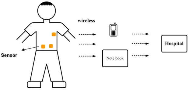
In the design of transmitter front-end, efficiency and linearity are the two most important factors. Efficiency, especially for low-power applications such as biomedical and portable devices, is a critical index, since it pinpoints the amount of wastage of the battery power. Low-power techniques on CMOS technology attract great attentions mostly on biomedical applications due to its compact and low-cost characteristics compared to the existing bulk and costly equipments. Sensors along with low-power RF front-ends facilitate the construction of body-area network (BAN) which provides real-time health monitoring in the future. BAN connects the remote patients or elderlies with hospitals for decreasing accidents and providing emergency services.
1.2 Body Area Network
Nowadays, technique is more and more developed. The equipments of medical become smaller and smarter. Therefore, people can carry sensors to monitor their health by means of wireless applications. The wireless sensor network is consisted of a few sensor nodes. Each node is able to transfer health information to local area network or cell phone. Some impediments of wireless sensor network have to be overcome. The things patients care about not only reliable data transfer but also the battery lifetime. The ultra low power consumption is necessary for extending the battery lifetime. The consideration of low power consumption could make users more convenient, and it could also reduce more energy loss.
1.3 Thesis organization
A quadrature frequency tripler with fundamental cancellation is presented in Chapter II. Introduction and motivation are described in section 2.1. The design consideration and circuit implementation are explained in section 2.2, followed by the measurement considerations and experimental results in section 2.3 and 2.4 respectively. A summary is given in section 2.5.
The design of the outphasing low-power PA is presented in Chapter III. Introduction to outphasing technique and the techniques for linearity and efficiency enhancement are provided in section 3.1 and 3.2 respectively. Then, the introduction to PAs and design considerations of class-D PAs are given in section 3.3 and 3.4 respectively. The power combining of outphasing PA is described in section 3.5, followed by the circuit implementation in section 3.6. The chip layout and post-layout simulations are demonstrated in section 3.7. Finally, section 3.8 summarizes the outphasing PA.
Chapter II
A Quadrature Frequency Tripler with Fundamental
Cancelling
2.1 Introduction and Motivation
Many frequency triplers have been proposed to utilize a nonlinear device, transistors for instance, to acquire the third-order harmonic by driving the transistors into a strongly non-linear region [2-4]. Then a filter is usually implemented in the next stage to eliminate undesired spurs at the output. In general, these circuits usually consume much power and have low conversion efficiency. Alternative method is proposed in [5], which is a time-wave form shaping technique. It enhances the third-order harmonic by pulling the output voltage three times in each fundamental cycle. This approach becomes less efficient in millimeter-wave frequencies limited by the switching operation of transistors. Similar approach was found in [6]. But it results in large power consumption and more complication.
In this work, frequency tripler with a technique of fundamental cancelling was proposed. By applying this technique, the third-order harmonic can be produced under low power consumption. In addition, the proposed technique forms a quadrature phase signal suitable for communication system with I/Q signals, which is good for image rejection.
According to the measured results, this frequency tripler with fundamental cancelling provides 35 dB harmonic rejection ratio (HRR) under 11.5 mW power consumption and conversion gain of -4.2 dB after calibrating poly-phase filter and
buffer loss. The phase noise measured at 1 MHz offset of the 1.5 GHz input signal source and the third-order output are -142.3 dBc/Hz and -123.8 dBc/Hz
Circuit realization is mentioned in Section 3.2. The measurement considerations are mentioned in Section 3.3, and chip implement and measurement results are in Section 3.4 circuit realization. The summary is given in Section 3.5.
2.2 Circuit Realization
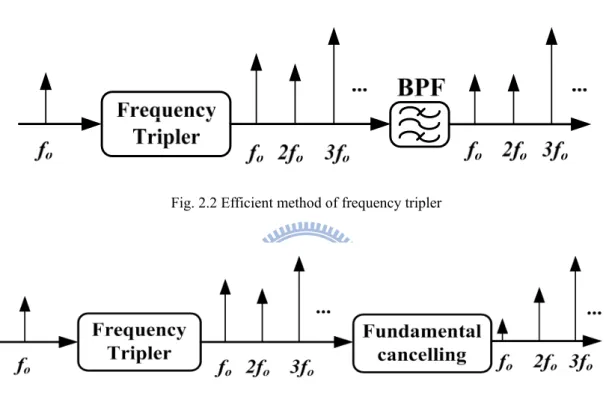
As aforementioned, typically the method relies on strong input signals that drive a device into the strongly nonlinear region to obtain the high-order frequency harmonics, of which the desired output signal is selected by filtering. It is confronted with large power consumption and large chip size for band-pass filter (BPF). Fig. 2.1 demonstrates traditional method of frequency tripler. Then the efficient method of frequency tripler was proposed that improved the conversion efficiency shown in Fig. 2.2.
The function of a frequency tripler not only produces the desired third-order harmonic but it also needs to have a high harmonic rejection ratio (HRR). In this work, the fundamental frequency cancelling is introduced that operates under low power consumption and saves BPF at output shown in Fig. 2.3. Accordingly, a tripler with a high HRR is critical to suppress undesired spurs.
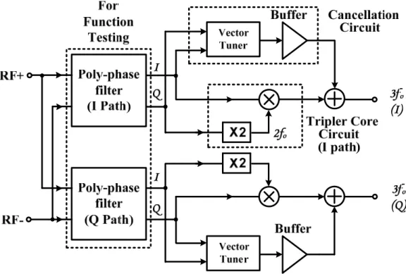
Fig. 2.4 shows the block diagram of the frequency tripler with fundamental cancelling. In circuit realization, it consists of a pair of poly-phase filter and a pair of frequency tripler with fundamental cancellation circuit. The poly-phase filter transforms the differential signal into quadrature I/Q signals. Then, the quadrature signals are injected into the core circuit to generate third-order harmonic signals at outputs. The quadrature generator, a pair of three-stage- poly-phase filters [10] are used in this work for function testing only. In circuit integration, the quadrature signals can be provided by a divider.
In this section, the frequency tripler, principle of fundamental cancelling and the evolution of the cancellation circuit will be mentioned.
Fig. 2.1 Traditional method of frequency tripler configuration
Fig. 2.2 Efficient method of frequency tripler
Fig. 2.4 The block diagram of frequency tripler with fundamental frequency cancellation
2.2.1 Frequency Tripler
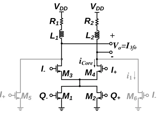
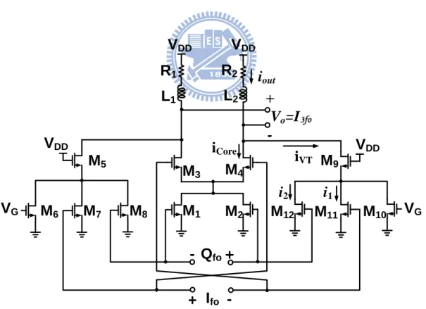
The frequency tripler was realized by injection of a second harmonic current [7]. Applying this technique, third-order harmonic can be generated efficiently under low power consumption. Fig. 2.5 shows the frequency tripler for I path and Q path. The bottom transistor pair, M1,2 or M13,14, forms a frequency doubler that provides a
second-harmonic current injection into the source-couple differential pair, M3,4 and
M15,16, which works like a switching stage of a conventional mixer. Therefore signals
with fundamental and third order harmonic frequencies (2fo±fo) are produced at output.
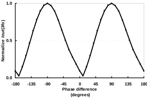
The most critical factors for maximizing 3rd harmonic current at the output are as follows. First, each transistor is biased at where the device could generate maximum gm’, which is the derivative of the transconductance gm. This will maximize the efficiency of frequency conversion. Second, the input phase difference
between top and bottom transistor are ±90 degrees out of phase that provides a maximal output current at 3fo shown in Fig. 2.6. These currents then flow through resistive loadings to produce the output voltages. There is a figure of merit, called harmonic rejection ratio (HRR), which indexes the performance of multiplier circuits. It is defined as the ratio of the desired harmonic to undesired n-th order harmonic, as demonstrated in Equation (2.1). ) harmonic order th -n Undesired harmonic Desired log( 20 ≡ HRR (2.1)
In frequency tripler circuit, the desired harmonic is the third-order one, and the undesired harmonic are fundamental and second order harmonics. Other higher order harmonics are small and have neglected effects on the circuit performance.
0.0 0.5 1.0 -180 -135 -90 -45 0 45 90 135 180 Phase difference (degrees) N o rm a iliz e I out (3f o )
Fig. 2.6 Output current at 3fo versus phase difference of upper and bottom difference pairs
2.2.2 Principle of Fundamental Cancelling
Although, the frequency tripler could produced the third-harmonic current efficiently, but it still exists many undesired harmonic signals especially of fundamental frequency. Equation (2.2) demonstrates the output current of frequency tripler. ... ) ψ ωt ( C ) ψ ωt ( B ) ψ t ( A
it = 1cos
ω
+ 1 + 1cos 2 + 2 + 1cos 3 + 3 + (2.2)where the A1cos (ωt+ψ1) , B1cos (2ωt+ψ2) and are fundamental, second-order and third-order harmonic signals.
) ψ ωt (
C1cos 3 + 3
In order to obtains higher harmonic rejection ratio in multiplier circuit.The filter is one of the most popular methods to suppress undesired spurs at output. It needs higher quality factor of filter that achieves higher harmonic rejection ratio, but it is not easy implemented in chip. Therefore, the fundamental frequency cancelling technique comes out to leave out the output filter.
The principle of fundamental cancelling is generating an inverse current at fundamental frequency then the output current at fundamental frequency could be cancelled. The current of cancellation circuit is expressed in equation (2.3).
... ) ωt ( C ) ωt ( B ) t ( A
ir = 2cos
ω
+θ
1 + 2cos 2 +θ
2 + 2cos 3 +θ
3 + (2.3)where the A2cos(ωt+θ1) , B2cos(2ωt+θ2) and C2cos(3ωt+θ3) are
fundamental, second-order and third-order harmonic currents.
According to equation (2.2) and (2.3), the output fundamental current would be cancelled completely while the θ1 =π +ψ1 and A2 = A1. Fig. 2.7 illustrates the concept of the fundamental cancelling.
Fig. 2.7 Concept of the fundamental cancelling
2.2.3 Evolution of Cancellation Circuit
Before going into the evolution of cancellation circuit, we should care the phase of the fundamental current of tripler. Because of the bottom differential pair (Fig. 2.5) forms a frequency doubler providing the second-order harmonic current injection into
source couple differential pair. Therefore, the output fundamental current of the frequency tripler is contributing from source couple differential pair. Therefore, a straight forward method is introducing a common source (CS) amplifier, M5 and M6,
then the CS amplifier connected to outputs that the input signals are 180-degree out of phase with source couple differential pair as demonstrated in Fig. 2.8. According to simulation result, the output fundamental currents of the tripler generating can be suppressed successfully but performance of the fundamental harmonic rejection ratio is not impressive. Because of parasitic capacitance are different that result in the current i1 and icore are not 180-degree out of phase, therefore, the current ioutwould not
be cancelled completely.Fig. 2.9 shows the frequency response of current of i1 , icore
and iout from 1 GHz to 2 GHz at Cartesian coordinate. The current iout is linear
combination of current i1 and icore.
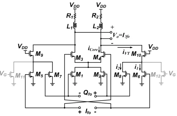
In order to enhance the fundamental rejection ratio another common source amplifier, M7 or M8, is introduced in cancellation circuit as shown in Fig. 2.10.
Consequently, the output fundamental current of the cancellation circuit iVT’, iVT’ is
linear combination of i1 and i2, can be adjusted by biasing point of transistors M5, M7
and M6, M8 but increased the parasitic capacitance at drain-source junction. The unit
current gain buffers (M9 and M10) are introduced to reduce the loading effect on the
tripler core due to the parasitic capacitance from the cancellation circuit. Fig. 2.11 illustrates the simulation result of output fundamental current (black), gray is previous simulation without current i2, of cancellation circuit and frequency tripler from 1 GHz
to 2 GHz. Moreover, transistors (M5, M7 and M6, M8) are biasing at sub-threshold
region, it is advantageous in low power consumption.
Finally, transistors (M11, M12) are introduced in cancellation circuit to provide
magnitude and phase of cancellation circuit at fo are decision by i1 and i2, then its illustrated in (2.4) and (2.5). 2 ) ( 2 2 ) ( 1 2 i fo i fo A = + (2.4) ) ( tan ) ( 1 ) ( 2 1 1 fo fo i i − + =π θ (2.5)
According to (2.4) and (2.5), the perfect cancellation occurs only at single frequency point. Therefore, the fundamental cancellation method is a narrow band configuration.
M
2
M
1
R
1
R
2
L
1
L
2
M
3
M
4
V
DD
V
DD
+
V
o
=I
-I
-
I
+
Q
-
Q
+
M
6
M
5
I
+
I
-i
Core
i
1
Fig. 2.8 Straight forward method
M
2M
1R
1R
2L
1L
2M
3M
4M
5M
7M
10M
9M
6M
8V
DDV
DDi
Corei
VTV
DDV
DD+
V
o=I
-- Q
fo-+ I
foi
1i
2Fig. 2.10 Improving HRR1 by adding another vector
+
Fig. 2.12 Schematics of proposed frequency tripler with fundamental cancellation for I path
-0.2 -0.1 0.0 0.1 0.2 -2 -1 0 1 2
Im (mA)
Re
(
m
A)
Iout (fo)
Icore (fo)
Icancel (fo)
2.3 Measurement Considerations
Based on the analyses in Section 2.2, an S-band fundamental cancelling circuit was designed and fabricated. Before going into the part of chip implementation, we ought to pay attention to some considerations relating to the final measurement. This step may determine what you can measure (or not) the actual results of your fabricated circuits.
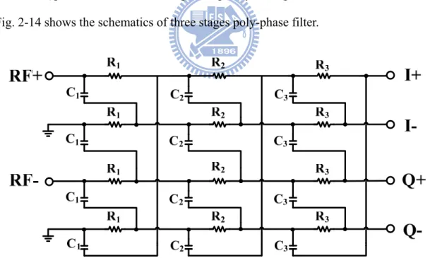
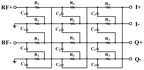
It is difficult to ensure quadrature phase signals because the mismatch of cables and adapters when they connect to the chip usually results in large phase errors and magnitude imbalance. For this reason, one pair of three stages poly-phase filters are merged into the tripler to provide the needed quadrature signals, one for I path the other for Q path. The fundamental input frequency is ranged from 1 GHz to 4 GHz. Fig. 2-14 shows the schematics of three stages poly-phase filter.
Fig. 2.14 Three stage poly-phase filter
It is very difficult to guarantee the phase and magnitude without mismatch because of the output signal path of the poly-phase filter is more complex to connect
into core circuit. To minimize the phase and magnitude error where the floating metal of fifth layer was introduced under metal of sixth layer that increasing parasitic capacitance (slow wave) as shown in Fig. 2.15. On the other hand, the process variation also should be considered. The capacitors and resistors are put together to minimize the process variation shown in Fig 2.16.
Fig. 2.15 Profile of poly-phase output path
Fig. 2.16 Poly-phase filter layout considerations for process variation
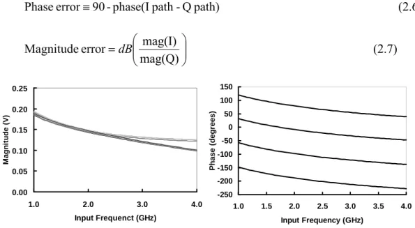
Fig. 2.17 illustrates the post layout simulation results of magnitude and phase frequency response from 1 GHz to 2 GHz input frequency of three stages poly-phase filter, and of magnitude and phase error are shown in Fig 2.18 that less than 0.4 dB and 0.3 degree, respectively. The phase error and magnitude error are defined as (2.6) and (2.7)
path) Q -path phase(I -90 error Phase ≡ (2.6) ⎟⎟ ⎠ ⎞ ⎜⎜ ⎝ ⎛ = mag(Q) mag(I) error Magnitude dB (2.7) 0.00 0.05 0.10 0.15 0.20 0.25 1.0 2.0 3.0 4.0 Input Frequenct (GHz) M a g ni tude ( V ) -250 -200 -150 -100 -50 0 50 100 150 1.0 1.5 2.0 2.5 3.0 3.5 4.0 Input Frequency (GHz) P h ase ( d eg rees)
Fig. 2.17 Frequency response of magnitude and phase
0.0
0.2
0.4
0.6
0.8
1.0
1.2
1.4
1.6
1.8
2.0
Input Frequency (GHz)
M
agn
it
u
d
e er
ro
r (
d
B
)
-0.1
0.0
0.1
0.2
0.3
P
h
ase er
ro
r (
d
eg
ree)
2.4 Chip Implement and Measurement results
A pair of frequency tripler with fundamental cancelling was realized in this work. The cancellation circuit was designed to produce out of phase signals with respect to tripler that can be used to cancel output fo current. This tripler features quadrature signals at both the input and output. The filter(s) that eliminated unwanted harmonics at output or off-chip was absent. In addition, a pair of poly-phase filter is also implemented for verifying the function of the frequency tripler.
2.4.1 Chip Implementation
As aforementioned, the output signal path of the poly-phase filter is more complication. In chip implementation, two poly-phase filters of three stages are fabricated in this work in view of layout considerations and I and Q path mismatch.
The frequency tripler with fundamental cancelling is fabricated using 180 nm standard CMOS technology. The total chip area, including one pair of three stages poly-phase filter (for function testing) one for I path and the other for Q path, two S-band frequency triplers with fundamental cancelling, four output buffers (for measurement), is 1400x1100 um2. The core circuit only occupied 350x1100 um2 and total power consumption of tripler in operation is 11.5 mW under 14 dBm input power (after calibrating cable and Hybrid loss), while output buffer consumes 43.1mW, all for 1.8 V supply voltage.
Fig. 2.19 Poly-phase filter for I path
M
2M
1M
6R
1R
2L
1L
2M
3M
4M
7M
8M
10M
9M
11M
12V
DDV
DDi
Corei
VTM
5V
DDV
DD+
V
o=I
-+
- Q
fo-+ I
foV
GV
Gi
1i
2i
outFig. 2.21 Poly-phase filter for Q path
+
Fig. 2.22 Frequency tripler with fundamental cancelling for Q path
2.4.2 Measurement Results
The Microphotograph of fabricated chip is shown in Fig. 2.23, and Fig. 2.24 illustrates measurement setup. An off-chip 180o hybrid coupler provides a differential
signal to pair of three stages poly-phase filter then the core circuit is driven by quadrature I/Q signals. Both I/Q paths, open-drain buffers are used for measurement purposed.
Fig. 2.24 Measurement setup
The HRR1 is one of the most critical performance what we care. Fig. 2.25 shows
a snapshot of the measured output spectrum with an input signal of 14 dBm (excluding cable and Hybrid coupler loss) at 1.5 GHz input frequency. The output power of the third-order harmonic is -23.7 dBm after calibration of cable loss.
Measured at the input frequency of 1.5 GHz, the output phase noise at third-order harmonic frequency is -123.8 dBc/Hz at 1MHz offset as shown in Fig. 2.26. The phase noise of the input signal is -142.3 dBc/Hz, yielding to discrepancy of 8.9 dB relate to the ideal multiplication. Fig. 2.27 shows the fundamental harmonic rejection ratio versus input power with a 1.5 GHz input signal. The HRR1 is more than
35 dB while input power is 14 dBm. Fig. 2.28 demonstrates the output power of fundamental and third-order harmonics versus input frequency. The conversion voltage gain versus input frequency is shown in Fig. 2.29, and Fig. 2.30 shows conversion voltage gain versus input power. The poly-phase filter and output buffer loss were calibrated which is 12.8 dB and 11 dB (simulation) respectively.
) , , log( 20 3 fo fo Vi Vo CG≡ ×
Fig. 2.25 Output spectra at 1.5 GHz with 19 dBm input power
-5
5
15
25
35
45
10
11
12
13
14
15
16
Input power (dBm)
HRR1
(
d
B)
Fig. 2.27 HRR1 versus input power
-70
-60
-50
-40
-30
-20
-10
0
1
1.1 1.2 1.3 1.4 1.5 1.6 1.7 1.8 1.9
Input Frequency(GHz)
O
u
tput P
o
w
e
r (dB
m
)
fo 3fo-8
-6
-4
-2
0
1
1.1 1.2 1.3 1.4 1.5 1.6 1.7 1.8 1.9
Input Frequency (GHz)
C
o
n
ver
si
o
n
G
a
in
(d
B
)
Fig. 2.29 Conversion voltage gain versus input frequency without poly-phase and buffer loss
Input frequency=1.5 GHz
-45
-41
-37
-33
-29
-25
-21
9
10
11
12
13
14
15
16
Input Power (dBm)
C
onve
rsi
on G
a
in
(d
B
)
Finally, a performance summary is given in the Table 2.1. The proposed frequency tripler with fundamental cancelling provides high HRR1 and moderates
conversion gain and lower power comparison. The comparison is given in the Table 2.2.
Table 2.1 Performance summary
Technology CMOS 180nm Power Supply 1.8 V DC Power (With Buffer) 11.5 mW (43.1mW) Fundamental Rejection Ratio 35 dB Conversion Gain -4.2dB Chip Area (Core circuit) 1400x1100 um2 (350x1100 um2)
Table 2.2 Comparison with other published
[6] [7] [8] [9] This work
Technology CMOS
180 nm 180 nmCMOS SiGe HBT pHEMT 180 nm CMOS Frequency (GHz) 1 7 8 12.67 1.5 HRR1 (dBc) 30 22.4 7 30 35 Conversion Gain (dB) 3 -5.6 -8 -3.4 -4.2 DC Power (mW) 68 7.5 92.4 14.7 11.5 w/o buffer
2.5 Summary
A novel frequency tripler with fundamental cancelling circuit is realized using TSMC 180 nm CMOS technology. The proposed frequency tripler has high harmonic rejection ratio under low dynamic power consumption and does not need any filters either at output or off-chip. In addition, the proposed technique feature a quadrature phase signals that suitable for the communication system with I/Q signals for image rejection.
Chapter III
Outphasing Low-Power Amplifier
3.1 Introduction
Efficiency and linearity are the most critical factors for RF front-end power amplifiers (PA). The efficiency had to contend with linearity in typical power amplifier. There are many technology could improve the linearity or efficiency such as Cartesian feedback, pre-distortion, adaptive digital pre-distortion, feed-forward, and outphasing amplifier for linearity enhancement and Doherty amplifier, and bias adaption for efficiency improvement.
The feed-forward method provides excellent linearity and broad-band characteristics. However, the error amplifier is a complicated control circuit [11]-[13]. The instability and bandwidth limitation is advantageous for feedback technique [14]-[16].
Outphasing modulation system is one solution to improve both efficiency and linearity that proposed by H. Chireix [17]. Outphasing PA is made up of a pair of power amplifiers and a combiner to combine signal. Class D power amplifier is used in this work that provides high efficiency (switched-mode power amplifier), and combiner is used transformer at output.
In section 3.2 mentioned the principle of outphasing transmitter, and introduction of Class D PA in Section 3.3. In section 3.4 illustrated circuit realization of class D power amplifiers. The combiner is a key factor of outphasing system. Therefore outphasing power combining technology was illustrated in Section 3.5. The circuit realization and chip layout and post-layout simulation were illustrated in Section 3.6
3.2 Outphasing Transmitter
The concept of LInear amplification with Nonlinear Component (LINC) or outphasing is that an amplitude and phase modulated signal is resolved into two out phased constant envelope signals by signal component separator. Fig. 3.1 shows the structure of the outphasing transmitter.
Fig. 3.1 Outphasing transmitter configuration
3.2.1 The Theory of Outphasing Amplification
The arbitrary input signal Vin(θ) is separated into two out phased constant
envelope signals V1(φ(t)) and V2(φ(t)), as illustrated in (3.1) (3.2) and (3.3).
)
cos(
)
(
)
(
t
=
A
t
ω
t
+
θ
V
in (3.1) )) ( ( max 1(
(
))
t t je
B
t
V
ϕ
=
ω +θ+ϕ (3.2) )) ( ( max 2(
(
))
t t je
B
t
V
ϕ
=
ω−θ+ϕ (3.3)))
(
(
))
(
(
)
(
t
V
1t
V
2t
V
out=
θ
+
ϕ
+
θ
+
ϕ
(
( ( )) ( ( )))
max t t j t t je
e
B
ω +θ+ϕ+
ω +θ−ϕ=
))
(
cos(
))
(
cos(
max maxt
t
B
t
t
B
ω
+
θ
+
ϕ
+
ω
+
θ
+
ϕ
=
=
2
A
(
t
)
cos(
ω
t
+
θ
)
(3.4) where(
)
cos
(
(
)
)
max 1B
t
A
t
=
−ϕ
In equation (3.4) presents principle of linear amplification. Fig. 3.2 illustrates the separation of two component signals from the source signal.
3.3 Power Amplifier Introductions
3.3.1 The parameters of power amplifier
definition
There are many parameters that can verify the performance of power amplifier. The definition of these parameters is shown below:
1. Drain Efficiency: The drain efficiency is defined as
= ×100%, DC out Drain P P η (3.5) where the Pout is the output power that delivered to load at the interesting frequency.
And the PDC is the total power consume from power supply. Ideally, the drain
efficiency is 100% for switched-mode power amplifiers.
2. Power Added Efficiency (PAE): The power added efficiency is most commonly used to verify the performance of power amplifier. It is defined as
= − ×100%, DC in out P P P PAE (3.6) where Pin is input power of power amplifier.
3. Input 1-dB compression point (IP1-dB): An amplifier keeps a constant gain for
low input power levels. Nevertheless, at higher input power levels, the amplifier goes into saturation and its gain decreases. The IP1-dB is referred to as the input power level
which results in 1 dB gain degradation form its small-signal behavior shown in Fig. 3.3.
4. Adjacent Channel Power Ratio (ACPR): The unwanted signal power at adjacent channel would be generated due to the nonlinear effect of the power amplifier. ACPR is a parameter which characterizes the ratio between signal power at the desired channel and adjacent channel. Higher ACPR means better isolation with
adjacent channel.
Fig. 3.3 P1-dB definition
3.3.2 Principle of Class D power amplifier
The efficiency is the most critical factor for power amplifiers design. Ideally, the drain efficiency achieves 100% for switched-mode power amplifiers, which is the transistor treated as a switch. Thus, transistor’s drain current and voltage never cross at the same time. Fig. 3.4 (a) shows the configuration of voltage-switching class D power amplifier [18]. It consists of an inverter and an L-C series resonator. The L-C tank removes the high-order harmonic frequency signal ensures sinusoidal output.
The transistor Mn and Mp are switched alternately that depend on input voltage
swing. The transistor Mn is turned on while the input swing is higher than its threshold
voltage. Then the voltage at the drain Vd of transistor Mn and Mp will be pulled down
to ground. On the contrary, the input voltage swing of transistor Mn and Mp will be
pulled up to VDD. Fig. 3.4 (b) and (c) present the pull up and pull down operation
mode. Fig. 3.4(d) shows the ideal waveform for power amplifier at the drain. During T1 period VD is pulled down to zero, and during T2 period, the NMOS is cut off and ID
power dissipation of the switch mode power amplifier is zero.
(a)
(c) Time Time Id PMOS ON NMOS ON PMOS ON NMOS ON (d)
Fig. 3.4 (a) Configuration of voltage-switching class D power amplifier(b) Pull down operation mode. (c) Pull up operation mode. (d) Ideal waveform at drain of transistor.
3.3.3 Switched mode low-power amplifier design considerations
There are many parameters ought to take care in low power amplifier circuit design.
1. Input voltage swing: As aforementioned, the input voltage swing must be large enough to fully turn on and off the transistor for a proper switched-mode power amplifier operation. The drain efficiency degrades with insufficient input voltage
swing. Fig. 3.5 shows the relationship between the voltage waveform at the drain and the input voltage swing. The sinusoidal waveform indicates an insufficient input voltage swing, while the square waveform corresponds to a sufficiently large input voltage swing which is able to fully turn on and off the transistor.
Fig. 3.5 Relationship between the voltage waveform at the drain and the input voltage swing
2. Output load impedance: The output load impedance of the power amplifier is a critical factor for the output power. The output power can be calculated by
load out out
R
V
P
2
2=
(3.7) where the Pout, Vout and Rload are the output power, root mean square output voltageand output load impedance, respectively. The smaller output load impedance leads to a larger output power transfer which is evident in (3.7). Usually, most output load impedance of power amplifier is decided by load-pull, which is the maximum output power can be found on a smith chart. For smaller output power level amplifiers, or said low power amplifiers, the small output load impedance is unnecessary.
at drain-source junction would result in switching speed reduction in high frequencies. Moreover, this Cp causes the energy dissipation due to CpVon2/2 where Von is output
voltage of transistor at the instant of switch closure, and the energy dissipated in the on-resistance of the transistor.
4. Finite turn-on and turn-off time of transistors: Ideally the device switched between the saturation mode with zero on resistance and the pitch off mode with zero drain current. However, in real transistors there would exist non-zero transition times overlapping between the drain current and voltage waveforms as illustrated in Fig. 3.6, especially at high frequencies. This results in efficiency degradation.
3.4 Circuit Realization of Class D power amplifier
3.4.1 Self biasing
Fig. 3.7 (a) shows the configuration of class D amplifier with self-biasing resistor. A large resistor, Rf, which connects across gate and drain is used to ensure a same DC
voltage potential of VG and VD while separating their ac behavior. The bias voltage at
gate and drain is VDD /2 while the total size of transistor Mn and Mp is 200 µm and 720
µm respectively.
3.4.2 Maximum Drain Efficiency
As mention previously, the small output load impedance is not necessary in low power amplifier circuit design, and the efficiency is the most important parameter that we care about. Therefore, the output load impedance of class D power amplifier is chosen to be 50 ohm for maximum drain efficiency (impedance transformation network is not necessary) at an input voltage swing of 0.3 V. Fig. 3.7 (b) shows the drain efficiency versus the output load impedance. The drain efficiency is more than 60%. Ideal components are used in this simulation except transistors. The transient response of the drain voltage and current of NMOS are shown in Fig. 3.7 (c) and (d). The overlapping of current and voltage result in efficiency degradation.
(a)
45
50
55
60
65
20
25
30
35
40
45
50
55
60
RL (ohm)
D
rai
n
ef
fi
ci
en
cy (
%
)
(b)0.0 0.2 0.4 0.6 0.8 1.0 1.2
0.0
0.5
1.0
1.5
Time (ns) Vd (V) (c) 0.0 2.0 4.0 6.0 8.0 10.0 12.0 14.00.0
0.5
1.0
1.5
Time (ns) Vd ( V ) (d)Fig. 3.7 (a) Class D amplifier with self-biasing resistor (b) Drain efficiency versus output load impedance (c) Transient response of drain voltage (d) Transient response of drain current
3.5 Outphasing Power Combining Technology
3.5.1 Combiner Types
There are many types of combiners for the outphasing power amplifier, including transformers, hybrid couplers, Wilkinson combiners, Lange couplers, and transmission line combiners. Among all, there are two types of combiners that are commonly employed at the output stage for power combining purpose. One is the lossless and unmatched combiner and the other is lossy and matched combiner.
The lossless and unmatched combiners provide high combining efficiency, unfortunately the linearity are poor. Chireix and Wilkinson combiner with isolation resistor are of this type. On the contrary, the lossy and matched combiners provide high isolation between combining ports, this yield high linearity but with poor combining efficiency, especially for the signal with high peak to average ratio. Table 3-1 summarizes these two types of combiners in terms of isolation, linearity, and efficiency.
Table 3-1 Comparison of lossy and lossless combiner
Isolation Linearity Efficiency
Lossy Good Good Bad
Lossless Bad Bad Good
3.5.2 Time Dependence of Input Impedance
The output of the two PAs can be written as two voltages that connected to the ))) ( sin( )) ( (cos( )) ( ( 1 V e V t j t V j t t m m in ψ ψ ψ ω = + = + (3.8)
))) ( sin( )) ( (cos( )) ( ( 2 V e V t j t V j t t m m in = ω−ψ = ψ − θ (3.9)
two input ports of combiner shown in Fig. 3.8 (a). Fig. 3.8 (b) illustrates the equivalent circuit and the input impedance Zin1 and Zin2 is drivenas below. The input
impedance that the resistive component is equal 2
L
R
. In (3.10), also see the capacitive and inductive reactance, which is a function of the input phase offset angle
ψ, meaning that the capacitive and inductive component is produced by phase
difference between two input signals.
(a)
(b)
Fig. 3.8 (a) Two input ports of combiner (b) The Norton equivalent circuit of the pair of series outphasing voltage sources
It can be derived as L m L in in out R t V R V V i = 1+ 2 =2 cos(ψ( )) )) ( sin( ) ( cos( )) ( cos( 2 1 1 t j t t R i V Z L out in in = = ψ ψ + ψ )) ( tan( 1 ( 2 j t RL + ψ = (3.10) ))) ( sin( ) ( (cos( )) ( cos( 2 2 2 t j t t R i V Z L out in in = = ψ ψ − ψ )) ( tan( 1 ( 2 j t RL ψ − = (3.11)
The reactance of Zin1 and Zin2 may lead to efficiency degradation. Chireix
combiner was proposed to improve the efficiency by adding parallel compensating components at the cost of linearity degradation. The Chireix combiner and its small-signal equivalent circuit are illustrated in Fig. 3.9 (a) and (b).
(b)
Fig. 3.9 (a) Chireix combiner (b) Equivalent circuit
The jB is the admittances of the compensating components.
According to Kirchhoff’s low, the current can be expressed as (3.12)
jB e V i i j m out ψ − − = 1 (3.12) jB e V R t j m L ψ ψ − − = 2cos( ( ))
After using Ohm’s low the input admittance could be calculated as (3.13)
) 1 )) ( cos( 2 ( 1 1 1 jB e R t V i Y j L in = = ψ − ψ (3.13) Therefore, the input impedance is inversion of (3.13).
) )) ( cos( 2 ( ) )) ( cos( 2 ( 1 1 1 1 ψ ψ ψ
ψ
ψ
j L j j L in in jBe R t e jB e R t Y Z − = − = =)) ( cos( ))] ( sin( )) ( cos( 2 [ ))) ( sin( )) ( (cos( )) ( cos( 2 ( t jBR t B R t e R t j t jB R t e L L j L L j ψ ψ ψ ψ ψ ψ ψ ψ − + = + − =
{
}
2 2 [ cos( ( ))] ))] ( sin( )) ( cos( 2 [ )) ( cos( ))] ( sin( )) ( cos( 2 [ t BR t B R t t jBR t B R t e R L L L L j L ψ ψ ψ ψ ψ ψ ψ + + + + =The maximum efficiency would be obtained while the imaginary part of Zin1 and Zin2
equal to zero. 0 ) Im(Zin1 =
(
cos( ( ))+ sin( ( )))
{
[2cos( ( ))+ sin( ( ))]+ cos( ( ))}
=0⇒RL ψ t j ψ t ψ t RLB ψ t jBRL ψ t
))
(
(
sin
))
(
(
sin
))
(
2
sin(
t
R
B
2t
R
B
2t
L Lψ
ψ
ψ
+
=
−
⇒
LBR
t
=
⇒
sin(
2
ψ
(
))
LR
t
B
=
sin(
2
ψ
(
))
⇒
(3.14) The (3.14) expresses the maximum efficiency in our interesting phase what the compensating component value is.There is a simple simulation where the phase offset is chosen in 0 and 45 degrees. Both the characteristic impedance and output loads is 50 ohm. While the compensate phase at 0 degree that do not need compensating component and the compensating phase at 45 degrees, according to (3.14) the Lcom and Ccom are 1.613 nH and 630 fF
respectively. Using the Chireix combiner would improve the efficiency in outphasing modulation system. Fig. 3.10 shows the efficiency enhancement by adding parallel compensating components but it leads to linearity degradation. Many researcher were analysis this topic in [19-21]. This would be further discussed in Section 3.4.4.
3.5.3 Efficiency and Linearity
1. EfficiencyThe instantaneous efficiency of the Chireix combiner was driven by [19] shown in (3.15)
(
)
2 2 2 2 2 4 2 2 1(1
2
y
cos
(
'
))
y
(
-
sin(2
'
))
)
'
(
cos
y
8
,
θ
β
θ
θ
θ
η
+
+
=
+
≡
in in outP
P
P
B
(3.15)0.0
0.2
0.4
0.6
0.8
1.0
0
10
20
30
40
50
60
70
80
90
Input phase difference (degree)
C
o
mb
in
er
E
ff
ici
en
c
y
0 degree 45 degree (B) (A)Fig. 3.10 Compensating phase (A) 0 degree (B) 45 degree
where Pout is the power transfer to the output load, and Pin1 and Pin2 are two available
powers at the input of the combiner and y is RL/Zo.
As mentioned in the previous section, with the use of compensating components, the reactive elements can be eliminated, resulting in the maximum transfer efficiency. The equation (3.15) can be simplified to
2 2 2 2 2 )) ' ( cos y 2 (1 ) ' ( cos y 8 ) ' , ( θ θ θ β η + = (3.16)
Equation (3.16) is the best condition for all compensating phase. While the characteristic impedance of λ/4 transmission line is equal 50 ohm. Then the (3.17) can be written as 2 2 2 max )) ' ( cos 2 (1 ) ' ( cos 8
θ
θ
η
+ = (3.17)The optimal efficiency of combiner, shown in Fig, can be calculated for all input phase offset angle θ by equation (3.17). Fig. 3.11 shows the optimal efficiency achieves 80% above while the compensating phase is from 0 degree to 63 degrees.
0
20
40
60
80
100
0
10 20 30 40 50 60 70 80 90
Input phase offset (degrees)
E
ff
ici
en
cy (
%
)
Fig. 3.11 The optimal efficiency of combiner for all input offset angle
Because of equation (3.16) is a function of Zo and θ. There are two cases for y>1 and y<1.
Case1: y>1
According to (3.16), we recalculated the optimal efficiency for all input offset angle. Then we obtained the optimal efficiency of combiner shown in Fig. 3.12. The optimal efficiency could achieve 100% at the higher input offset angle. But the optimal efficiency is quiet low at the lower input offset angle.
Case1: y<1
0
20
40
60
80
100
120
0
10
20
30
40
50
60
70
80
90
Input phase offset (degrees)
E
ff
ici
en
cy (
%
)
Fig. 3.12 (a) Zo is 20(b) Zo is 30 (c) Zo is 400
20
40
60
80
100
120
0
10
20
30
40
50
60
70
80
90
Input phase offset (degrees)
E
ff
ici
ency (
%
)
Fig. 3.13 (a) Zo is 60. (b) Zo is 70.We recalculated the optimal efficiency for all input offset angle and plot the curve of the optimal efficiency again shown in Fig. 3.13 It is flat and quite high after adding compensating components, but the optimal efficiency is dropped rapidly while the input offset angle is larger 50 degrees.
2. Linearity
There is a trade-off between efficiency and linearity, sine adding compensating components would degrade the linearity of the Chireix combiner [22]. Fig. 3.14 illustrates the effect of the compensating phase on the linearity. Perfect linearity occurred while compensating angle is zero thereafter the distortion is more evident while the compensating angle increases.
0.0
0.2
0.4
0.6
0.8
1.0
1.2
0.0
0.2
0.4
0.6
0.8
1.0
Normailized Vin (V)
N
o
rm
a
iliz
e
d
V
o
u
t (V
)
Fig. 3.14 Effect of compensating angle at the linearity of Chireix combining system (a) w/o (b)15 degrees (c) 45 degrees and (d) 75 degrees
3.6 Circuit Realization
The proposed outphasing class D low-power amplifier is shown in Fig. 3.15. The transistor Mn1/Mp1 or Mn2/Mp2 forms a class D power amplifier which amplifies the
input signals to the combiner. The transformer is used to combine the signals providing by two path of class D power amplifier. Further discussions about class-D power amplifier and transformer will be presented in section 3.6.1 and 3.6.2.
Fig. 3.15 Schematics of outphasing power amplifier
3.6.1 Combiner comparisons?
The Wilkinson combiner is first used in outphasing technique in this work. Fig. 3.16 (a) and (b) show the efficiency versus input offset angle and probability density function (PDF) of the OFDM modulation system respectively. The drain efficiency is simulated under ideal Wilkinson combiner. In OFDM modulation system, the PDF is most located at 70 degrees, which the efficiency dropped severely. Therefore, it degraded the average efficiency significantly. After calculation, the average efficiency is only 13 percents only for ideal Wilkinson combiner. Then the Chireix combiner is chosen to improve the efficiency by adding compensating components at 70 degrees.
But it results in severe linearity degradation. This is the fundamental trade-off between efficiency and linearity of a power amplifier.
In this work we used the transformer combining two input signals. The maximum efficiency of transformer will be 180 degrees. Fig. 3.17 shows the efficiency of transformer without phase compensation for linearity consideration.
Fig. 3.16 (a) The efficiency of the Wilkinson combiner V.S input offset angle (ideal combiner) (b) The PDF of the OFDM modulation system
0.0
0.2
0.4
0.6
0.8
1.0
0
15
30
45
60
75
9
Input phase angle (degrees)
N
or
m
a
iliz
e
d output
v
olt
a
ge
(
V
0
)
Fig. 3.17 Combiner Efficiency versus input offset angle using transformer
3.6.2 Why class-D power amplifier?
There are many types of switched-mode power amplifier including class D、class E and class F etc. The efficiency of these amplifiers can in principle be excellent. The reasons of choosing class D power amplifier mentioned as below.
The characteristics of the Class E amplifiers are not appropriate to outphasing systems with lossless power combiner. Because of the characteristic of zero-voltage switching is critically dependent on the phase of the output load impedance. Therefore, the class E amplifiers are best suited for lossy combiners [18].
For class-F power amplifier, both efficiency and output power are boosted by using harmonic impedance in the output network. The load of even harmonics frequency (2fo, 4fo…) must be low impedance and odd harmonics (3fo, 5fo…) frequency must be high impedance except fundamental frequency [22]. It is difficult to realize the impedance at each harmonic frequency for fully on chip design,
moreover the more harmonics impedance result in more loss at the output.
The class-D power amplifier does not have zero-voltage switching and harmonics impedance issue of class-E and class-F amplifiers. For those reasons we chosen class D power amplifier.
In this work we care the average efficiency of the outphasing power amplifier more than PA performance.