Wednesday / 198
CWF22
New method of fabrication of remnant photonic photonic band gap ~ t ~ U d n r f % bssed on the polymer nlms MIIbiniIIg multivalent mre-eaRh metal caiioat formed by stepwire
alternate adsorption of m e a l cations and plyanioos. I.Beresneva,G.Khomutov,B.1.Mantsyrov,I.A.O~heredov.A.P.Shkurinov P h p c r Oeparrnrenr and I~emorional h e r Cenlw, M KLomommv Marcow State
U n w e m i ~ , Moscow, 119899, Rursro P.l&wliQ G-Mwret
Lobomrolm de PhysicuChimie de I’Amarphh, EP 1831 CNRS m 1 D . 14s ovenue Mowice Schumnn, Uniwr~ird du Lilfwczl, 59140. Dunkerque, Fmnce The last years have wimcssed an intense investigation of light popqaiirm in periodic smctures. These structures are usually referred to as photonic hand gap (PBG) crystals. These c r y s ~ A s have many practical applications in optics and technology.
In this presentation we dermk the method of fabrication of PBG materials that may have penodic modulation of r e f d o n mdex. ahsorption coefficient and the nonlineaity .s well.
The method is h a d on thc layer-by-layer self-assembly technique that has been widely studied for the p-se of surface modification and far the construction of new inorganic, hybrid organic/inorgarUc and polymer-based materials with nanoxalezrmtmlled mucture and prapetties. In this contribution we present results of a study of polymeric films and the multilayer structures on its basis with very high content of multivalent metal ations formed by tahng advantage of stepwise cmrdination of polyanion and multivalent metal cations, m
paniculsrly, trivalent rare-earth metal cations The method of film fabrication is baxd on the layer-by-layer membly and alternate adsorphon of metal eations and polyelectrolite molecules containing negatively charged l q m d p u p s to form condensed supramolecular structure with integrated wmplexes of metal rations In this approach multivalent metal cations are intrinsically structure-forming component without which resulting matcrial can not be formed Such film dissolved slowly being placed in an a q m w eldrolite solution. The purpaseful variations of polper morphology, its functional @oups chemical specificity and structure give possibilities for effective propertydtiven design of metal cation complexes tn such material and effective material perty tailoring The interactions of B number of m- eafih metal Cations (Gdj’, E?. Nd’ywith pulyanionr (poly(styrenesulfonate), poly(acrylic acid)) have been studied and corresponding polymeric films with very high rar~earth cations content (about 70.80% weight) were successfully formed.
Layer-by layer film growth procedure in this method is relatively simple and manufacturable, and allows for the systematic effective nanamcfecscalf level control of chemical mnlenf cmpition, funCtiondicy. metal cation complexes slmmre and 6lm thickness This structure, in tum, determiner film properties of interest (optical, elemonic, mechanical, ek.), As a result, such polymer rareearthdoped film materials can be perspective for various photonic applications.
We studied films with dimerent rare-earth metal cations and the one dimensional PBG srmctwes based on the selfassembled film using the steady-state linear optical methods. We also sN&ed its nonlinenr optical properties ming Second Harmonic and Sum-frequency Generation techtuques using tunable femtosecond laser sources
CWF23
Metal-Oxide-Semiconductor Light-Emitting Diodes a t Si Bandgap Euergy Miin-Jang Chen, Ching-Fuh Lin, Jiann Jong Chin, Cheewee Liu
and Shu-Wei Chang Department of Electrical Engineering
and
Graduate lnstitute of Electro-Optical Engineering National Taiwan University
Taipei 106, Taiwan ROC
Tel: 886-2-2363525 I ext. 339iFax: 886-2-23638247
Silicon is the most popular material for electronics industry. Howcver. its applications in optics and optoelectronics are not as popular, mainly limited by the indirect-bandgap characteristics of silicon. Due to the mature fabricalion processing technology, it is highly desired to make Si emit lidit. Although many methods had been invented to generate electroluminescence from Si [ I
1,
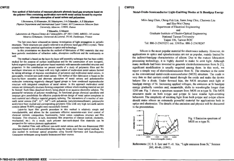
significant modification is usually required among them. In this work, we report a simple way of electroluminescence from Si. The structure is the same as the conventional metal-oxide-semiconductor (MOS) s h u c t v e . The oxide ISv e y thin so that carriers could tunnel through the oxide and make the device behave like a diode. Under forward bias, the MOS structure emit light at bandgap energy of Si. Increasing applied voltages, the emission at Si bandgap energy gradually vanishes and, meanwhile, shifts to wavelengths longer
than
1200 om. Fig. 1 shows a spechum measure from MOS on n-type Si. The MOS simctwes made on both n-type and p t y p e Si have similar light-emitting behaviors. The simplicity of emitting light ftom both p-type and n-type silicon should make silicon an extremely powerful material for applications both in optics and electronics. The details of the emission and physics will be discussed in the presentation.
Fig. I Emission spectrum of
MOS on n-type Si.
References: [I] S. S. Iyer and