行政院國家科學委員會專題研究計畫 成果報告
高性能長壽命可撓式有機薄膜電晶體元件之製作與研究(I) 研究成果報告(精簡版)
計 畫 類 別 : 個別型
計 畫 編 號 : NSC 96-2221-E-011-144-
執 行 期 間 : 96 年 08 月 01 日至 97 年 07 月 31 日 執 行 單 位 : 國立臺灣科技大學電子工程系
計 畫 主 持 人 : 范慶麟
計畫參與人員: 碩士班研究生-兼任助理人員:林昶志 碩士班研究生-兼任助理人員:林育生 博士班研究生-兼任助理人員:楊宗憲
處 理 方 式 : 本計畫涉及專利或其他智慧財產權,1 年後可公開查詢
中 華 民 國 97 年 10 月 29 日
高性能長壽命可撓式有機薄膜電晶體元件之製作與研究(I)
“Investigation and fabrication of flexible organic thin film transistor devices with high performance and long lifetime (I)”
計畫編號:NSC96-2221-E-011-144
執行期間:96 年 08 月 01 日 至 97 年 07 月 31 日 主持人:范慶麟 台灣科技大學電子工程系副教授
I. 中文摘要
本計劃利用 N2O 電漿針對有機薄膜電晶
體(OTFTs)之低溫沉積 SiO2閘極絕緣層進行表
面處理,研究結果顯示 N2O 電漿處理技術可
降低的 SiO2 之表面粗糙度並改善有機主動層
材料–pentacene 結晶特性,亦可降低元件之 trap-state density , 以 提 高 有 機 薄 膜 電 晶 體 (OTFTs)元件效能。藉由此電漿處理技術,可 提升 OTFTs 元件之載子移動率大於 50%,並 減少 31%之 trap-state density。
關鍵字:有機薄膜電晶體、氧化亞氮電漿、閘 極絕緣層、載子移動率、缺陷密度。
Abstract
The electrical characteristics of N2O-plasma treated pentacene thin-film transistors are investigated. The treatment can enhance the on current almost two times, increase the field-effect mobility (μFE) greater than 50%, and reduce the interface traps to 31%, compared to devices without plasma treatment. This improvement is presumably owing to pentacene crystallisation enhancement and the decreased traps state density between the pentacene and gate dielectric interface. The N2Oplasma treated gate dielectric has been found effective in improving organic thin-film transistor (OTFT) performance.
Keywords: Organic thin film transistor (OTFT), N2O-plasma treatment, gate dielectric, field-effect mobility, trap-state density.
II. INTORDUCTION
Organic and polymer material based electronic devices have attracted much attention in recent years. This interest can be attributed to the emerging demand for novel electronic devices such as radiofrequency identification tags, smart cards and display media on low cost and/or flexible substrates.
The surface roughness of the gate dielectric is an important factor that affects the electrical performance of organic semiconductor films in thin film transistors (TFTs), especially in field effect mobility [1]. Many studies have focused on decreasing the surface roughness of the gate dielectric and growing pentacene to form polycrystalline [1, 2]. Recently, Kwan et al. [3]
reported on an NH3-annealing thermally grown gate dielectric (SiO2) that might be an effective way to decrease gate dielectric surface roughness and improve OTFT performance. However, the OTFT device is generally fabricated at a low temperature. The NH3-annealing gate dielectric is therefore not suitable for the organic thin-film transistor. In addition, it has been reported that interface trap state density (Nt), such as dangling
bonds or weaker bonds, between gate dielectric (SiO2) and pentacene active layers are also key issues affecting the performance of OTFTs [4, 5].
Therefore, several schemes have been devised to reduce the trap state for pentacene-based OTFTs [4, 5]. Here we present a new technique for treating the OTFT gate dielectric with N2O-plasma. This method is a low temperature process that can produce a smooth gate dielectric surface and simultaneously reduce the interface trap state, resulting in significant improvement in device performance. To our knowledge, this is the first time N2O-plasma has been applied in treating the gate dielectric and improving OTFT performance.
III. EXPERIMENT
The pentacene-based OTFTs used a bottom contact (BC) structure, fabricated onto a heavy doped n-type silicon substrate to act as the gate electrodes. The gate dielectric, 100 nm-thick SiO2 is grown using high density plasma chemical vapour deposition (HDP-CVD) at 375
˚C. The metal Pt/Cr (70 nm/2 nm) is evaporated using an electron-beam evaporation system as the source/drain (S/D) electrodes, which are patterned using the lift-off method onto the gate dielectric before N2O-plasma treatment. For the structure using N2O-plasma treatment, the device is subjected to pure N2O-plasma at 200 mTorr for 10 min in a HDP-CVD chamber with non-heated substrate. The device channel length and width are 4 μm and 500 μm, respectively.
We deposited the organic films in the non-heated substrate by thermal evaporation using pure pentacene powders. The pentacene film thickness was about 700 A˚ and the deposition rate was fixed at ~0.3 A˚/s.
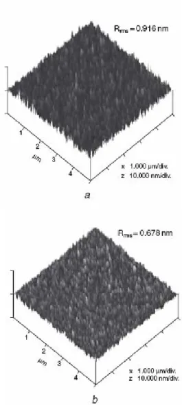
Fig. 1 AFM images of gate insulator SiO2 without and with N2O-plasma treatment
a Without N2O-plasma treatment b With N2O-plasma treatment
IV. RESULTS and DISCUSSION
Fig. 1 illustrates the AFM images of the gate dielectric (SiO2) surface without and with N2O-plasma treatment, where the root-mean-square values of surface roughness (Rrms) were determined to be 0.916 and 0.678 nm, respectively. It had been reported that a significant decrease in gate dielectric (SiO2) surface roughness after oxygen plasma treatment was observed as a result of the oxygen cleaning effect [6]. Fritz et al. reported that upon gate dielectric smoothing prior to pentacene
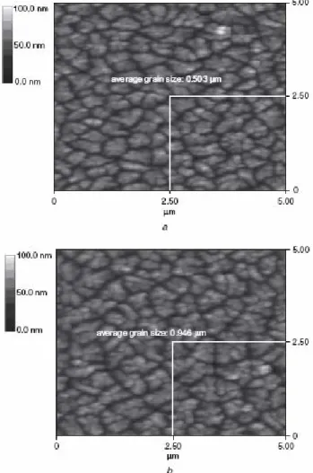
deposition, dramatic enhancement in pentacene grain sizes were observed [1]. Thus, we established that the dissociated oxygen radicals from the N2O-plasma can decrease the gate dielectric (SiO2) surface roughness and produce large pentacene grain size, as shown in Figs 2a and b, respectively. The pentacene grain size (average grain size is 0.946 μm) with N2O-plasma treatment is larger than that without treatment (average grain size is 0.503 μm).
Fig. 2 AFM images of pentacene films on SiO2 without and with N2Oplasma-treatment
Average grain size calculated by selected area divided by amounts of grain
a Without N2O-plasma treatment b With N2O-plasma treatment
Figs 3a and b show the output characteristics of the pentacene-based OTFTs without and with
N2O-plasma treatment on the gate dielectric (SiO2) with different gate voltages (VGS), respectively. The magnitude of the device on current without and with N2O-plasma treatment is 0.65 and 1.25 μA, respectively (at VGS = – 40 V, VDS = – 20 V). The device on current with N2O-plasma treatment is almost two times larger than that for the device without treatment. In addition, the field-effect mobility (μFE) can be calculated from the slope of the (IDS)1/2 plot against VGS in the saturation regime. The μFE of the device without and with N2O-plasma treatment is 7.69 × 10⁻³ cm2/Vs and 1.17 × 10⁻² cm2/Vs, respectively. It was found that the μFE of the device with N2O-plasma treatment is 50%
larger than the device without treatment.
Fig. 3 Output characteristics of pentacene-based OTFTs without and with N2O-plasma treatment
a Without N2O-plasma treatment b With N2O-plasma treatment
It is well known that SiO2 films deposited at low temperature have essentially lower atomic bonding energy during high-voltage stressing and the atomic bonds are apt to be broken, resulting in traps generated inside the oxide and at the oxide interface [2]. Therefore, the interface trap density will be an important factor that affects the electrical performance of OTFTs with low-temperature deposition gate dielectric.
The interface trap density is calculated and
extracted using the method of Levinson et al. [7]
and Proano et al. [8]. Using the N2O-plasma treatment, the trap state density was reduced from 1.61 × 10¹³ to 1.1 × 1013 cm–2. This decreased trap state density is believed to be due to nitrogen radicals dissociated from the N2O-plasma and introduced into the gate dielectric (SiO2) surface. This phenomenon results in the formation of strong Si-N bonds that replace the dangling bonds or weaker bonds of the gate dielectric surface and reduce interface traps. The increased strong Si-N bonds will result in OTFT performance improvement, especially in the on/off current ratio and field-effect mobility [2]. Thus, the fabricated pentacene-based OTFTs with N2O-plasma treated gate dielectric show better performance than those without gate dielectric treatment, including higher field-effect mobility and higher saturation current.
V. CONCLUSION
We investigated the N2O-plasma effect on the gate dielectric (SiO2) properties of OTFTs based on pentacene. The N2O-plasma treatment successfully reduced gate dielectric (SiO2) roughness and simultaneously improved pentacene crystallisation. The pentacene-based OTFTs with N2O-plasma treatment can improve the on current almost two times, increase the μFE
greater than 50%, and reduce the interface traps
to 31%, compared to devices without plasma treatment. Therefore, we believe that N2O-plasma treatment is a good candidate method to improve OTFT performance.
VI. REFERENCES
[1] Fritz, S.E., Kelley, T.W., and Frisbie, C.D.: ‘Effect of dielectric roughness on performance of pentacene TFTs and restoration of performance with a polymeric smoothing layer’, J. Phys. Chem. B, 2005, 109, pp.
10574–10577.
[2] Park, S.K., Kim, Y.H., Han, J.I., Moon, D.G., and Kim, W.K.: ‘High performance polymer TFTs printed on a plastic substrate’, IEEE Trans. Electron Devices, 2002, 49, pp. 2008–2015.
[3] Kwan, M.C., Cheng, K.H., Lai, P.T., and Che, C.M.:
‘Improved carrier mobility for pentacene TFT by NH3 annealing of gate dielectric’, Solid-State Electron., 2007, 51, pp. 55–58.
[4] McDowell, M., Hill, I.G., McDermott, J.E., Bernasek, S.L., and Schwartz, J.: ‘Improved organic thin-film transistor performance using novel self-assembled monolayers’, Appl. Phys. Lett., 2006, 88, pp. 073505 [5] Myny, K., Vusser, S.D., Steudel, S., Janssen, D.,
Mu‥ller, R., Jonge, S.D., Verlaak, S., Genoe, J., and Heremans, P: ‘Self-aligned surface treatment for thin-film organic transistors’, Appl. Phys. Lett., 2006, 88, pp. 222103.
[6] Lee, M.W., and Song, C.K.: ‘Oxygen plasma effects on performance of pentacene thin film transistor’, Jpn.
J. Appl. Phys., 2003, 42, pp. 4218–4221.
[7] Levinson, J., Shepherd, F.R., Scanlon, P.J., Westwood, W.D., Este, G., and Rider, M.:
‘Conductivity behavior in polycrystalline semiconductor thin film transistors’, J. Appl. Phys., 1982, 53, pp. 1193–1202.
[8] Proano, R.E., Misage, R.S., and Ast, D.G.:
‘Development and electrical properties of undoped polycrystalline silicon thin-film transistors’, IEEE Trans. Electron Devices, 1989, 36, pp. 1915–1922.
VII. 計畫成果自評
本計畫利用N2O電漿處理技術降低以低溫沉積之SiO2閘極絕緣層的表面粗糙度、改善有機主動
層材料–pentacene結晶特性與降低trap-state density,以提高有機薄膜電晶體(OTFTs)元件效能,與原 計 畫 目 的 相 符 、 並 達 成 預 期 與 目 標 , 目 前 本 計 劃 研 究 成 果 已 投 稿 至 國 際 期 刊 IET (IEE) ELECTRONICS LETTERS並已被刊登(Vol. 44, No. 19, pp. 1158-1160, 2008.),此外亦投稿至IEDMS 2007國際性會議一篇。
可供推廣之研發成果資料表
□ 可申請專利 ■ 可技術移轉 日期:97 年 10 月 29 日
國科會補助計畫
計畫名稱:高性能長壽命可撓式有機薄膜電晶體元件之製作與研究 (I) 計畫主持人:范慶麟
計畫編號:NSC 96-2221-E-011-144 學門領域:微電子學門 技術/創作名稱 以 N2O 電漿處理有機薄膜電晶體之低溫沉積 SiO2閘極絕緣層 發明人/創作人 范慶麟
中文:
本計劃利用 N2O 電漿針對有機薄膜電晶體(OTFTs)之低溫沉積 SiO2閘
極絕緣層進行表面處理,研究結果顯示 N2O 電漿處理技術可降低的 SiO2
之表面粗糙度並改善有機主動層材料–pentacene 結晶特性,亦可降低元 件之 trap-state density,以提高有機薄膜電晶體(OTFTs)元件效能。藉由 此電漿處理技術,可提升 OTFTs 元件之載子移動率大於 50%,並減少 31%之 trap-state density。
技術說明 英文:
The electrical characteristics of N2O-plasma treated pentacene thin-film transistors are investigated. The treatment can enhance the on current almost two times, increase the field-effect mobility (μFE) greater than 50%, and reduce the interface traps to 31%, compared to devices without plasma treatment. This improvement is presumably owing to pentacene crystallisation enhancement and the decreased traps state density between the pentacene and gate dielectric interface. The N2Oplasma treated gate dielectric has been found effective in improving organic thin-film transistor (OTFT) performance.
可利用之產業 及 可開發之產品
1. 有機薄膜電晶體與低溫複晶矽薄膜電晶體。
2. 主動驅動液晶顯示器。
3. 主動驅動有機電激發光顯示器。
技術特點
1. 利用 N2O 電漿處理可降低 SiO2表面粗糙度
2. 利用 N2O 電漿處理可降低元件的 trap-state density。
3. 利用 N2O 電漿處理可提高元件效能。
推廣及運用的價 值
利用 N2O 電漿處理技術降低以低溫沉積之 SiO2閘極絕緣層的表面粗糙
度、改善有機主動層材料–pentacene 結晶特性與降低 trap-state density,
以提高有機薄膜電晶體(OTFTs)元件效能。
※ 1.每項研發成果請填寫一式二份,一份隨成果報告送繳本會,一份送 貴單位研發成果 推廣單位(如技術移轉中心)。
※ 2.本項研發成果若尚未申請專利,請勿揭露可申請專利之主要內容。
※ 3.本表若不敷使用,請自行影印使用。