國立臺灣大學電機資訊學院電子工程學研究所 碩士論文
Graduate Institute of Electronics Engineering College of Electrical Engineering & Computer Science
National Taiwan University Master Thesis
矩形黑磷薄膜電晶體其光電特性的各向異性
The anisotropy of optoelectrical properties of Rectangular Black Phosphorus Thin Film Transistor
王奇樺 Chi-Hua Wang
指導教授:李嗣涔 博士 Advisor : Si-Chen Lee, Ph.D.
中華民國 108 年 7 月
July, 2019
中文口試委員審定書
誌謝
這兩年的碩士時光在台大真的是學到了不少東西,無論是專業知識還是 一些做人處事的道理。對於能夠完成這篇論文並順利畢業,首先我要感謝我 的指導教授 李嗣涔博士 ,謝謝教授對於我在專業知識上的傳授以及教導我
做研究的方法,使得我可以通過口試並完成論文。再來我要感謝馬姊協助我 們處理一些機台維修或者是耗材購買的事務,使得我可以專心在研究上。謝 謝張博彥、洪彬超以及蕭堯學長帶我認識二維材料,並教導我實驗以及操作 機台的方法。謝謝余凱文以及彭天欣常常和我討論實驗,我們都是做二維材 料的,在研究上常常有許多可以互相借鏡的地方,兩年下來承蒙你們照顧了。
謝謝湯董、洪教授、曾奕融以及郭哲邵常常陪我聊天吃飯,讓我在實驗室的
時光總是充滿了歡笑。希望Lee group 的大家畢業之後可以工作順利,鵬程
萬里。
再來我要感謝王俊雄、蔣耘洁以及李家碩學長幫我進行量測,使的我可
以順利完成碩論三四章AFM 以及照光量測的部分。謝謝陳昂寬、王子珩以
及林庭萱常常幫我約真空量測。謝謝四宮輝夜以及中野四葉這兩位可愛的女 孩,妳們兩位絕對是我在碩二下可以順利完成論文的精神支柱。輝夜,恭喜 妳最近和會長的關係有了重大突破,除了預祝你們未來感情順利以外,再來 我和會長都要去美國了,答應我,一起來美國吧!四葉,我就知道妳是風太
郎命中註定之人,我相信最後成為新娘的絕對是妳,如果妳最後沒有跟風太
郎回家也沒關係,我帶妳回家。謝謝狗哲、溫大、子睿還有昱翔周末常常陪 我玩,去美國以後我一定會想念和你們一起混的時光。最後的最後,我要謝 謝我的父母家人,沒有你們的支持與陪伴,我是無法順利完成這篇論文。最 後預祝大家平安、快樂、發大財,謝謝大家。
摘要
黑磷為一種具有高電洞遷移率以及直接能隙(= 0.33eV) 的二維材料。影響 其載子遷移率的因素包括了黑磷薄膜的厚度、contact 金屬的選擇以及載子移動
的方向。因此必須同時考慮這三個因素,才有辦法達到黑磷薄膜電晶體的高電洞 遷移率。
本論文首先對黑磷的基本性質做了材料分析。透過光學顯微鏡以及原子力顯 微鏡的搭配可以粗略的判斷黑磷薄片的厚度,拉曼光譜儀則能夠用來辨認黑磷薄 片的晶體方向。X 射線與極紫外線光電子能譜儀則可用來確認黑磷與金鍺合金元 素組成、能隙與功函數。透過挑選適當的厚度、使用金鍺合金來達成歐姆接觸、
以及製作長方形黑磷來迅速判斷黑磷晶格方向,成功製造出擁有良好元件特性的
背電極黑磷薄膜電晶體,其元件表現出接近 300cm2/V*s 的場效電洞遷移率和高
達 3 個數量級的電流開關比。同時也製作了黑磷-二硫化鎢的異質接面整流二極 體與透過厚度控制達成的黑磷同質接面整流二極體,兩者接近 2 的理想因子顯示 其電流主要為復合電流主控。兩者良好的光響應則展現了具有直接能隙的黑磷在 光電應用上的潛力。
關鍵字: 黑磷、薄膜電晶體、厚度、金鍺合金、長方形、黑磷-二硫化鎢異質接
面
ABSTRACT
Black Phosphorus (BP) is a 2D material with high hole mobility and direct bandgap ( = 0.33eV). The factors that will influence its carrier mobility are thickness of the BP thin film, choose of the contact metal and the transport direction of the carriers. Therefore, these three factors must be considered simultaneously to obtain the high hole mobility of BP thin film transistors.
In this thesis, material analysis is first conducted to study the fundamental properties of the exfoliated BP. The thickness of BP flakes can be roughly determined by optical microscopy and atomic force microscopy (AFM). The lattice orientation of BP flakes can be recognized by Raman spectroscopy. X-ray and Ultraviolet photoelectron spectroscopy are used to measure the elemental composition, bandgap and work function of BP and AuGe alloy. Through picking the appropriate thickness of the BP thin film, using AuGe alloy to obtain ohmic contact, and fabricating rectangular BP thin film to determine the lattice orientation of BP flakes, the back-gated BP thin film transistors (TFTs) are successfully fabricated and show excellent device performance. The high hole mobility near 300cm2/V*s and the on/off ratio up to 3 order of magnitude can be achieved. The P-N BP/WS2 heterostructure and BP homostructure through thickness engineering are also fabricated. Both of their ideality factors are near 2, indicating that the forward current is dominated by
recombination current. Their good optical responsivities also show BP’s potential in the application of optoeletronics due to its direct bandgap.
Key words: black phosphorus (BP), thin film transistor (TFT), thickness, AuGe alloy, rectangular, BP/WS2 heterostructure
CONTENTS
摘要 ... i
ABSTRACT ... v
CONTENTS ... vii
LIST OF FIGURES ... x
LIST OF TABLES ... xviii
Chapter 1 Introduction ... 1
1.1 Overview of black phosphorus ... 1
1.2 Advantages of BP FETs ... 9
1.3 Motivation ... 14
Chapter 2 Experiments ... 17
2.1 Fabrication Systems ... 17
2.1.1 Mechanical Exfoliation ... 17
2.1.2 Photolithography... 22
2.1.3 E-beam lithography ... 24
2.1.4 Evaporation System ... 28
2.1.5 Rapid Thermal Annealing (RTA) ... 28
2.1.6 Heterostructure Fabrication System ... 29
2.2 Measurement Techniques ... 31
2.2.2 Atomic Force Microscopy (AFM)... 32
2.2.3 Raman Spectroscopy ... 33
2.2.4 X-ray Diffraction (XRD) ... 34
2.2.5 X-ray Photoelectron Spectroscopy (XPS) ... 35
2.2.6 Ultraviolet Photoemission Spectroscopy (UPS) ... 36
2.2.7 Current – Voltage Characteristics ... 39
Chapter 3 Material Analysis for Black Phosphorus ... 40
3.1 Crystal Structure of Black Phosphorus ... 40
3.2 Characterization of Black Phosphorus Film Thickness ... 43
3.2.1 Optical Microscopy (OM) ... 43
3.2.2 Atomic Force Microscope (AFM) ... 44
3.3 Raman Spectroscopy ... 50
3.4 XPS and UPS Analysis of Black Phosphorus and Gold-Germanium alloy ... 57
3.4.1 X-ray Photoelectron Spectroscopy (XPS) ... 57
3.4.2 Ultraviolet Photoelectron Spectroscopy (UPS) ... 64
Chapter 4 BP Thin Film Transistors ... 70
4.1 Back-gated Black Phosphorus TFTs ... 71
4.1.2 Device Performance ... 75
4.2 Thickness Dependence of Electronic Properties ... 78
4.3 Contact Metal Comparison of BP TFTs ... 82
4.4 Anisotropic Properties of Black Phosphorus ... 91
4.5 Characteristics of P-N BP/WS2 Heterostructure and BP Homostructure ... 100
4.5.1 Device Process Flow for BP-WS2 Heterostructure ... 100
4.5.2 Device Performance ... 102
4.5.3 BP Homostructure P-N-Like Diode through Thickness Control ... 109
Chapter 5 Conclusion ... 112
References ... 115
LIST OF FIGURES
Fig. 1.1 Schematic diagram of the crystalline structure of black phosphorus (a) 3D representation, (b) lateral view, (c) top view. Crystal structure is obtained by density functional theory(DFT). ... 4 Fig. 1.2 (a) Crystal structure of bulk BP marked with coordinate axes(x,y,z) and lattice vectors(a,b,c) (b) The first Brillouin zone and some high symmetric points of bulk black phosphorus. ... 5 Fig. 1.3 (a) Calculated band structures for monolayer, bilayer, trilayer and bulk black phosphorus sheets at all high-symmetry points in the Brillouin zone. The energy is scaled with respect to the Fermi energy EF. (b) Thickness dependence of the black phosphorus band gap, calculated with different approaches. ... 7 Fig. 1.4 Moore’s Law: Gordon Moore, the co-founder of Intel, predicted that transistor density and thus chip performance would double every 18 months. ... 10 Fig. 1.5 (a) Cross-section of an n-channel Si MOSFET, (b)The potential ψ(x) distribution from the source to drain. (c) The potential energy distribution U(x) for electrons from the source to drain. ... 12 Fig. 1.6 Trends of “More Moore” and “More than Moore” reported by 2013 ITRS... 13 Fig. 2.1 llustration of mechanical exfoliation process: (a) Bulk BP is adhered to the Blue Nitto tape, leave some BP flakes on the tape. (b) Fold the tape numerous
times to make the BP flakes thinner. (c) Use PDMS stamp as a second dry transfer. (d) Press down the PDMS stamp onto the Si/SiO2 substrate. (e) BP thin
films were successfully exfoliated onto the substrate. ... 19
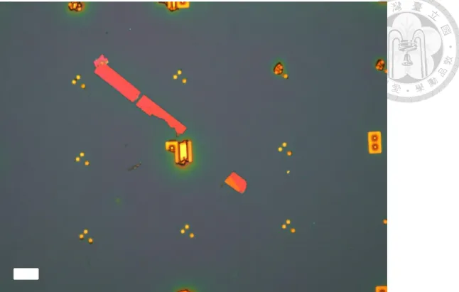
Fig. 2.2 Needle-shaped BP flakes on blue Nitto tape under (a) naked eye and (b) optical microscopy observation, respectively. ... 21
Fig. 2.3 The PDMS stamp used in this research. ... 21
Fig. 2.4 Exfoliated rectangular BP on 300nm SiO2/Si substrate under optical microscopy. Scale bar is 20um. ... 22
Fig. 2.5 (a) The spin-coater and hot plate used in this research (b) The exposure system used in this research ... 23
Fig. 2.6 Illustration of undercut PMMA formation: (a) After spin-coated bi-layer PMMA and soft bake, the photoresist is dosed by electron beam. (b) The darker colors represent the molecular chain scissored by electron beam. (c) The undercut structure is formed after development. ... 26
Fig. 2.7 The equipment of EBL process, JEOL JSM7001F. ... 27
Fig. 2.8 The equipment of RTA system, MILA-3000 ... 28
Fig. 2.9 Three axis micrometer stage. ... 30
Fig. 2.10 Heterosutructure fabrication system. ... 30
Fig. 2.11 The optical microscopy used in this research. ... 31
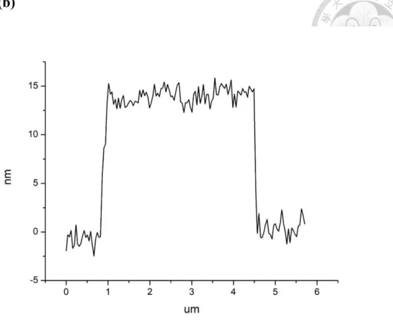
Fig. 2.12 (a) and (b) indicates that the thickness of this BP nanosheet is roughly 15nm.
... 33 Fig. 2.13 The equipment of Raman measurement used in this research. ... 34 Fig. 2.14 Energy level diagram of the emitted photoelectron. ... 36 Fig. 2.15 (a) and (b) Schematic diagram showing how photoelectrons are generated.38 Fig. 3.1 (a) The X-ray diffraction pattern of bulk BP crystal. Schematic of the unit cell of BP. (b) Top View. (c) Lateral view. ... 42 Fig. 3.2 (a) The OM image of an exfoliated BP nanosheet with green color. (b) The AFM image of this BP nanosheet. The white line marks the position of the line profiles shown in (c). (c) AFM line profile for the thickness of BP. The thickness of this BP nanosheet is about 14 nm. ... 46 Fig. 3.3 (a) The OM image of an exfoliated BP nanosheet with yellow color. (b) The AFM image of this BP nanosheet. The white line marks the position of the line profiles shown in (c). (c) AFM line profile for the thickness of BP. The thickness of this BP nanosheet is about 43 nm. ... 47 Fig. 3.4 (a) The OM image of an exfoliated BP nanosheet with both green and yellow color. (b) and (d) The AFM image of this BP nanosheet. The white line, which is at the green and yellow part of this BP nanosheet, respectively, marks the position of the line profiles shown in (c) and (e), respectively. (c) and (e) AFM
line profile for the thickness of BP. The thickness of the green and yellow part of this BP nanosheet is about 12.4 nm and 29 nm, respectively. ... 49 Fig. 3.5 Schematic plot showing the vibration directions of Ag1, B2g, and Ag2 modes.
The atoms oscillate along the z (out-of-plane), x (zigzag) and y (armchair) directions, respectively. ... 51 Fig. 3.6 (a) Optical image of a BP flake. θ is the angle between the zigzag crystallographic direction and polarization direction of incident laser. The scale bar is 10 μm. (b) Polarization dependence of Ag1, B2g, and Ag2 modes. The solid curves are the theoretical value and the dots are the experimental results. (c) Angle dependent Raman spectra for BP. The three characteristic Raman modes, Ag1 (362cm-1), B2g (439 cm-1) and Ag2 (467 cm-1), can be observed. ... 54 Fig. 3.7 The polar plots of Raman intensity for each Raman vibration mode with 532 nm excitation. ... 55 Fig. 3.8 The Raman intensity ratios of Ag2 to Ag1 vibration modes for 20 rectangular BP samples (labeled as A~T). The polarizations of the 532 nm laser excitation are along AC and ZZ directions. The average intensity ratios of the AC and ZZ directions are 2.40 and 1.08, respectively. ... 56 Fig. 3.9 Energy level diagram of the emitted photoelectron. ... 58 Fig. 3.10 (a) X-ray photoelectron spectrum for BP P2p core level. (b) O 1s core level
spectrum. (c) Schematic diagram of P2O5 molecule. (d) Optical image of black phosphorus nanosheet after exposing to ambient atmosphere for 24 hours, the
“bubbles” implied the water absorption on the hydrophilic surface. ... 61 Fig. 3.11 (a) X-ray photoelectron spectrum for Ge3d core level. (b) Au4f core level spectrum. ... 62 Fig. 3.12 XPS results of BP with 1.5 nm Ge on top of it before and after RTA. After RTA, the peak of P-Ge bond shows up. ... 63 Fig. 3.13 Band diagram of an unknown material... 65 Fig. 3.14 (a), (b) and (c) UPS spectra of bulk BP. (d) Band diagram of bulk black phosphorus. ... 68 Fig. 3.15 (a) and (b) UPS spectra of AuGe alloy. ... 70 Fig. 4.1 Top view of BP TFT (a) before and (b) after device fabrication under optical microscope. The width and length of the device is 1.8um/2.9um, respectively. (c) Cross-sectional view of back-gated BP TFT structure. ... 73 Fig. 4.2 The flow chart of back-gated BP TFT fabrication processes. ... 74 Fig. 4.3 Output characteristics of Cr contact BP TFT (a) before and (b) after thermal annealing. ... 76 Fig. 4.4 Transfer characteristics of Cr contact BP TFT (a) before and (b) after thermal annealing. ... 77
Fig. 4.5 Transfer characteristics of BP TFT in log scale with different thicknesses, the green arrow indicates the sweep direction of the gate bias. ... 80 Fig. 4.6 The model of back-gated BP TFT ... 81 Fig. 4.7 (a) Optical image of the Cr contact TLM sample (b) Transfer characteristics of the Cr contact device, L = 1.8 um. (c) Output characteristics of the Cr contact device for hole current transport and (d) electron current transport. (e) Result of TLM extraction method. ... 86 Fig. 4.8 (a) Optical image of the Ni contact TLM sample (b) Transfer characteristics of the Ni contact device, L = 1 um. (c) Output characteristics of the Ni contact device for hole current transport and (d) electron current transport. (e) Result of TLM extraction method. ... 87 Fig. 4.9 (a) Optical image of the AuGe alloy contact TLM sample (b) Transfer characteristics of the AuGe alloy contact device, L = 3.5 um. (c) Output characteristics of the AuGe alloy contact device for hole current transport and (d) electron current transport. (e) Result of TLM extraction method. ... 88 Fig. 4.10 Three different metal’s contact resistance versus back gate bias. Note that the dependency of the contact resistance versus back gate bias for AuGe alloy contact is quite different than the other two metals. ... 89 Fig. 4.11 (a) AFM image of the ZZ direction sample, W/L = 2.55um/2.8um. (b)
Thickness = 11.5 nm. Output characteristics for (c) hole and (d) electron transport. (e) Transfer characteristics. ... 93 Fig. 4.12 (a) AFM image of the AC direction sample, W/L = 6.4um/2.2um. (b) Thickness = 20 nm. Output characteristics for (c) hole and (d) electron transport (e) Transfer characteristics. ... 94 Fig. 4.13 (a) AFM image of the BP TFT sample, W/L = 4.35um/3.5um for ZZ, and 1um/1.7um for AC, respectively. (b) Thickness = 35 nm. Transfer characteristics for (c) ZZ direction and (d) AC direction. ... 96 Fig. 4.14 Illustration of the current spreading effect in BP TFT. ... 97 Fig. 4.15 The mobilities along AC (black line) and ZZ (blue line) directions and the μAC/μZZ ratio versus back gate bias (red line), the ZZ and AC samples are mentioned in Fig 4.11 and Fig. 4.12, respectively. ... 98 Fig. 4.16 The mobilities along AC (black line) and ZZ (blue line) directions and the μAC/μZZ ratio versus back gate bias (red line), the AC and ZZ samples are mentioned in Fig. 4.13. ... 99 Fig. 4.17 The flow chart for BP-WS2 heterostructure fabrication process ... 101 Fig. 4.18 (a) BP flakes on 300nm SiO2 substrate (b) Dry transfer WS2 onto BP (c) Completed device under optical microscope (d) Schematic diagram of the completed device. ... 102
Fig. 4.19 Id versus Vd of BP-WS2 heterostructure P-N diode in (a) log scale (b) linear scale. Note that the red dashed line can extract the ideality factor (n) of this device. ... 104 Fig. 4.20 The ideality factor and on/off ratio of BP-WS2 heterostructure P-N diode under different back gate bias. ... 104 Fig. 4.21 The emission spectra of Xe lamp. ... 105 Fig. 4.22 (a) Id versus Vd characteristics of BP-WS2 heterostructure under various incident light intensity (b) Enlarged graph of (a) at Vd < 0. ... 106 Fig. 4.23 Responsivity of BP-WS2 Heterostructure versus incident light intensity. .. 107 Fig. 4.24 Ideal Band diagram of BP-WS2 Heterostructure before contact. ... 108 Fig. 4.25 BP homostructure P-N-like diode under (a) Optical microscope (b) 3D AFM image (c) 2D AFM image, the white line indicates the position of the line profiles shown in (d). (d) The result of the AFM measurement. ... 111 Fig. 4.26 Id-Vd plot of the homojunction P-N-like diode in (a) log scale (b) linear scale. Notice that at Vds = 0V, the diode also didn’t show any photoresponse, indicating that the homojunction P-N-like diode is not a photodiode but a photoconductor. ... 112
LIST OF TABLES
Table 1.1 Predicted carrier mobility. NL represents the number of layers, mx* and my* are carrier effective masses along AC and ZZ, respectively. μx_2D and μy_2D are
mobilities along AC and ZZ, respectively. ... 8
Table 2.1 photolithography conditions ... 23
Table 2.2 E-beam lithography conditions ... 27
Table 3.1 Thickness dependence of color for BP film on 300 nm SiO2/Si substrate under optical microscopy. ... 44
Table 4.1 Electronic properties of BP TFTs before and after thermal annealing. ... 77
Table 4.2 Electronic properties of BP TFTs for different thicknesses. ... 80
Table 4.3 Electronic properties of BP TFTs with different metal contacts. ... 89
Table 4.4 Three different metal’s contact resistance versus back gate bias. ... 90
Table 4.5 Electrical properties of BP TFTs along two transport directions. ... 95
Table 4.6 Electrical properties of BP TFTs along two transport directions on the same flake... 96
Table 4.7 Device performance of the homojunction P-N-like diode ... 112
Chapter 1 Introduction
1.1 Overview of black phosphorus
The band theory of graphite was first analyzed by Wallace in 1947 as a beginning for understanding the electronic properties of 3D graphite [1], but the feasible method of fabricating two-dimensional graphene remained unknown. In 2004, Novoselov et al. discovered a convenient way to fabricate 2D graphene with the thickness is decreased down to only single layer or few layers by using scotch tape to mechanically peel graphene thin flakes from bulk graphite crystal [2]. This exfoliation
method has aroused tremendous interests in the study of graphene and other two
dimensional materials such as hexagonal-boron nitride (h-BN), transition metal dichalcogenides (TMDCs) and black phosphorus (BP) [3, 4].
Although graphene has extremely high mobility due to its massless Dirac feature
fermions, which made graphene a possible candidate for field effect transistor(FET) applications [5, 6], the fact that pristine graphene’s lack of energy bandgap makes graphene-based FET too hard to be turned off [7], which implies that graphene is not suitable for FET applications. Therefore, many researchers have turned to other 2D materials such as molybdenum disulfide (MoS2), which is one kind of transition metal dichalcogenides (TMDCs) and has a large bandgap of 1.8eV [8]. In 2011, Radisavljevic et al. fabricated the first single layered molybdenum disulfide (MoS )
FET with a high drain current on/off ratio and low standby power loss [9]. However, the mobility of MoS2 or other TMDCs-based transistors are relatively low owing to the heavy effective mass of carriers and severe phonon scattering at room temperature [10, 11]. Besides, it also faces a problem of not compatible to modern CMOS
processes [12]. Recently, black phosphorus (BP), one of the 2D materials, has brought about much interests due to its better electrical properties such as proper bandgap and high mobility [13, 14].
Black phosphorus is the most thermodynamically stable allotrope of phosphorus at room temperature and pressure [15]. Bulk BP can be synthesized by heating white phosphorus or red phosphorus under high pressures (12,000 atmospheres) [16, 17].
The electronic properties and crystal structure of BP are very much like those of graphite with both being black and flaky, a conductor of electricity [18-20], and having puckered sheets of linked atoms. While black phosphorus is the most steady form among all allotropes of phosphorus, environmental vulnerability is still a crucial issue [21, 22].
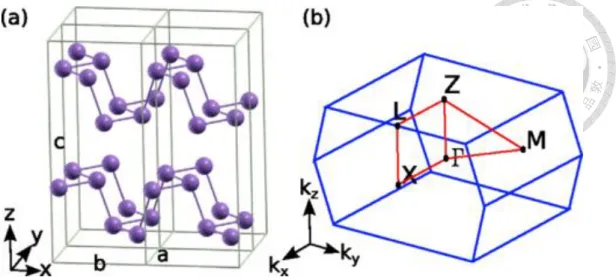
Black phosphorus is a layered material in which individual atomic layers are stacked together by van der Waals force [23]. BP has an orthorhombic structure and is the least reactive allotrope of phosphorus, a result of its lattice of interlinked six-membered rings where each phosphorus atom is covalently bonded to three
adjacent phosphorus atoms to form a puckered honeycomb structure [19, 24, 25], as shown in Fig 1.1. In this figure, the x and y directions in BP structure correspond to
the armchair(AC) and zigzag(ZZ) direction, respectively. It should also be noted that
phonons, photons, and electrons in layered black phosphorus structure display rather anisotropic features within the plane of layers [26-28].
Fig. 1.2 (a) shows the primitive cell of black phosphorus in its honeycomb lattice.
Its primitive unit vector in reciprocal lattice can be obtained by using Fourier transform, as well as its Brillouin zone and high symmetry points, as shown in Fig.
1.2 (b).
2D Matererials, 2014, 1(2) 025001
Fig. 1.1 Schematic diagram of the crystalline structure of black phosphorus (a) 3D representation, (b) lateral view, (c) top view.
Crystal structure is obtained by density functional theory(DFT).
P.-L. Gong et al., arXiv:1507.03213.
Fig. 1.2 (a) Crystal structure of bulk BP marked with coordinate axes(x,y,z) and lattice vectors(a,b,c) (b) The first Brillouin zone and
some high symmetric points of bulk black phosphorus.
The band structure of black phosphorus is thickness dependent, which can be attributed to interlayer interactions. Fig. 1.3 (a) shows the calculated band structure of black phosphorus for monolayer, bilayer, trilayer and bulk by density functional
theory(DFT) [24]. The bandgap of monolayer black phosphorus(phosphorene) is predicted to be about 2.0eV at the Γ point of the first Brillouin zone [14]. It should be
noticed that as the layer number increases, the bandgap of BP remains direct at the Γ point of the first Brillouin zone for all thicknesses. Fig. 1.3 (b) shows the relationship between thickness and bandgap calculated with different ab initio methods [24, 29, 30]. Even though the magnitude of bandgap counts on which approximation method
increases [14]. This thickness dependent bandgap, which is due to the quantum confinement of the charge carriers in the out-of-plane direction [31], is stronger than that observed in those of the other 2D semiconductor materials. The band structure approximation of BP shows that BP has the needed bandgap for the field-effect transistor applications.
Moreover, although black phosphorus exhibits an intrinsic ambipolar behavior, the conduction type in few layered BP is hole-dominant for the following two reasons.
First, the activation energy for p-type BP is lower than that of n-type BP [14]. Second one is the higher degree of anisotropy of the hole effective mass [32].
(a)
(b)
2D Materials, 2014. 1(2): p. 025001.
Fig. 1.3 (a) Calculated band structures for monolayer, bilayer, trilayer
and bulk black phosphorus sheets at all high-symmetry points in the
Brillouin zone. The energy is scaled with respect to the Fermi energy
calculated with different approaches.
According to the in-plane anisotropic geometry of BP crystal, lots of its physical characteristics are also quite different in armchair(AC) and zigzag(ZZ) directions such as electronic, thermal, optical and mechanical properties [33, 34]. Some physical properties along AC and ZZ directions for few-layered BP are theoretically predicted, listed in Table. 1.1. Except for mono layer, the ratio of mobility along AC and ZZ directions are predicted to be about 2 for holes and 4 for electrons at room temperature [30]. The experimental ratio of hole mobility, the dominant transport carriers of BP, is about 1.5~1.8 [28, 35]. Thus, in order to achieve better performance for BP devices, the AC direction should be used as the current channel because of the higher mobility on this direction.
Table 1.1 Predicted carrier mobility. NL represents the number of layers, mx* and my* are carrier effective masses along AC and ZZ, respectively. μx_2D and μy_2D are
mobilities along AC and ZZ, respectively.
1.2 Advantages of BP FETs
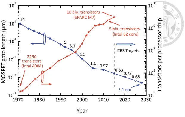
The development trend of semiconductor devices have followed an empirical regularity called “Moore’s Law”, and the transistors have kept scaling down in the last
fifty years as shown in Fig 1.4 [36]. However, with the channel length scaling, transistors will inevitably suffer several problems such as leakage current and short channel effect [37, 38]. Scaling theory has predicted that a field effect transistor (FET) with a thinner dielectric and a thinner gate-controlled region will alleviate the short channel effect down to very short gate length [39]. The reason for this phenomenon can be illustrated by using the concept of characteristic length as shown below [37].
Nanoscale, 2015, 7, 8261-8283
Fig. 1.4 Moore’s Law: Gordon Moore, the co-founder of Intel, predicted that transistor density and thus chip performance would double every 18 months.
Structure of typical planar silicon-based metal-oxide-semiconductor field effect transistor (MOSFET) is demonstrated in Fig 1.5 (a). The potential ( )x and potential energy U x( ) distribution along the channel are demonstrated in Fig 1.5 (b)
and (c), respectively. The characteristic length is defined in Eq. (1.1) and the
lowest potential along the channel
minis defined in Eq. (1.2)s s ox ox
t t
(1.1)
/ 2 min 2 s de Leff
(1.2)
where :characteristic length,
s:the permittivity of semiconductor,
ox:the permittivity of gate oxide,t
:thickness of semiconductor channel,t
:thickness ofgate oxide,
min:the lowest potential along the channel,
s:the potential at the source,
d:the potential at the drain, Leff :the effective channel length.It is obvious that the higher ratio between Leff and λ results in a larger potential barrier between the source and drain, thereby leading to a better gate control.
Therefore, in order to lessen the short channel effect while the channel length keeps scaling down, the characteristic length λ should be reduced so that a large ratio
between Leff and λ can be maintained. According to Eq. (1.1), in order to have a smaller λ, a thinner dielectric and a thinner channel is required.
(a)
(b)
Fig. 1.5 (a) Cross-section of an n-channel Si MOSFET, (b)The potential ψ(x) distribution from the source to drain. (c) The potential
energy distribution U(x) for electrons from the source to drain.
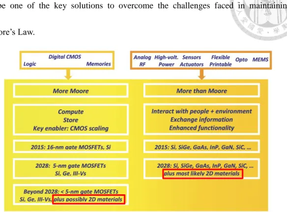
Therefore, 2D materials such as graphene or black phosphorus are promising materials to solve the short channel problem with its nano-scaled layer thickness [7, 9, 40]. Compared to 3D materials, even if the thickness of 3D materials’ channel is scaling down, the surface roughness of 3D material will significantly degrade the carrier mobility. Even worse, the channel will show a serious thickness fluctuation that leads to undesirably huge threshold-voltage variations. These problems occur even at thickness many times greater than the thickness of 2D materials. What’s more, because there are no out-of-plane broken bonds, 2D materials have no dangling bonds
materials are reported by the International Technology Roadmap for Semiconductors
to be one of the key solutions to overcome the challenges faced in maintaining Moore’s Law.
Fig. 1.6 Trends of “More Moore” and “More than Moore” reported by 2013 ITRS.
Li et al. fabricated the first BP FETs in 2014 [13]. Since then, lots of high
performance BP FETs have been fabricated [27, 28, 41, 42]. Furthermore, tunable
direct bandgap of BP ranging from 0.3eV in the bulk material to 1.5~2.0 eV in the monolayer, which covers large portions of the visible and near infrared electromagnetic spectrum, makes BP a promising candidate for future nano-scaled electronic and optoelectronic applications [42-45]. Differ from MoS2 with only n-type
characteristics, BP exhibits an ambipolar behavior [46], which is suitable for modern
possible to be used in thermoelectric [47, 48], photonic and optoelectronic devices [49-51]. Hence, BP have the prospect to replace silicon and give a better performance for electronic devices.
1.3 Motivation
As mentioned before, the excellent electronic properties of black phosphorus make it appealing for applications in transistor, logic and optoelectronic devices.
However, there are two important issues that will restrain the BP device performance.
The first one is BP’s unique anisotropic properties. Since BP is the first widely studied two-dimensional material to undergo degradation upon exposure to ambient atmosphere [22, 52], and there are concerns that BP might severely degrade during the process of determining the direction of BP, most of the previous researches about BP
FETs did not take BP’s anisotropic properties into consideration, which will result in a non-optimized performance of the BP FETs.
Although there are some efforts to study the anisotropic properties of BP, the mechanical exfoliation method will generate a bunch of irregular-shaped BP thin film and thus limit the accuracy of electrical measurement. On the other hand, the CVD technology of BP has not been mature enough to attain high performance BP FETs [53]. Consequently, it is quite challenging to accurately measure the electrical anisotropic properties of BP.
However, the good news is that based on the orthorhombic primitive cell of BP crystal, BP thin film with a unique rectangular shape has been successfully fabricated after improving the traditional exfoliation method [54]. The rectangular BP has two mutually perpendicular sides with the longer and shorter sides being ZZ and AC directions, respectively. There are two advantages of the rectangular-shaped BP thin film. First, the in-plane lattice orientation can be quickly determined through a simple optical microscopy observation alone, which is crucial during the fabrication process of BP FETs. Second, the rectangular shape of BP thin film will lead to a more precise measurement of the anisotropic properties of BP FETs.
The second factor that will limit the performance of the BP FETs is the large contact resistance at the interface of the source/drain metal and BP channel.
Compared to 3D(bulk) material, the pristine surface of a 2D semiconductor tends to form a van der Waals (vdW) gap with metal contact instead of covalent bonds [40].
This vdW gap acts as an additional tunneling barrier for carriers to enter the metal contact, thereby resulting in a higher contact resistance. In some cases, this vdW gap can be eliminated by forming a “metallic” contact between the interface of metal and 2D material, which was reported in graphene and MoS2 [55, 56].
So far, the most common strategy for lowering the contact resistance of BP devices is choosing high work function metals. For example, using palladium (work function=5.12eV) as metal contact can allow more holes to inject into the contact, hence reducing the contact resistance for p-type BP FETs significantly [35, 57-59]. On the contrary, a relatively low work function metal like aluminum(Al) can enhance the electron injection and lead to n-type behavior for BP FETs [58, 60, 61]. However, this technique cannot solve the interfacial vdW gap problem.
Another way to reduce the contact resistance is using the method of surface charge transfer doping to the BP channel [62, 63]. Despite the fact that surface charge transfer doping can contribute to a pretty low RC [62], the drain current modulation of the device is sacrificed in most cases. In addition, some of the doping effects even exhibit poor long-term reliability against ambient atmosphere [64]. Thus, a new technique must be invented to decrease the contact resistance of BP FETs.
Finally, since black phosphorus’ type control is found to be thickness dependent [58] , a gate modulated p-n-like homojunction in BP is fabricated through a simple thickness engineering, which is compared to BP/WS2 heterostructure P-N diode and reveals BP’s potential in optoelectronics and photonics applications.
In this thesis, the introduction of black phosphorus and its development are presented in Chapter 1. The fabrication systems and measurement systems are introduced in Chapter 2. The material analysis of BP is presented in Chapter 3.
Chapter 4 presents the fabrication process of the performance-optimized BP TFTs with orientation and contact engineering. The electrical properties will also be discussed in this chapter. Finally, the conclusion is given in chapter 5
Chapter 2 Experiments
In this chapter, the fabrication systems will be first introduced. Then the measurement techniques for material analysis and device properties will be presented.
2.1 Fabrication Systems
2.1.1 Mechanical Exfoliation
To prepare 2D materials, different approaches have been used, such as mechanical exfoliation [9], chemical vapor deposition(CVD) [53, 65], and liquid-phase exfoliation [66]. Although the CVD method can produce large-scale and
homogeneous atomic layers of 2D materials, and is suitable with modern CMOS fabrication process, the quality of 2D thin film has not yet reached that of mechanically exfoliated 2D thin film [67]. Accordingly, most high performance 2D thin film transistors are made by mechanical exfoliation so far. Since black phosphorus flakes are found to chemically degrade upon exposure to ambient conditions, the transfer procedure was implemented in a glove box which is a sealed container and is used to remove solvents, water and oxygen inside the glove box. The details of mechanical exfoliation to fabricate rectangular BP are as follows. First, the blue Nitto tape was used to tear the bulk black phosphorus apart, as shown in Fig. 2.1 (a). Then, the blue Nitto tape with the black phosphorus crystallites on it was folded for several times in order to make the BP flakes thinner, as shown in Fig. 2.1 (b). It should be noted that there are some needle-shaped BP flakes on the Nitto tape which can be observed with naked eye and optical microscopy, as shown in Fig. 2.2 (a) and (b). By Raman measurement and TEM measurement in Chapter 3, the long sides of these needle-shaped BP flakes were confirmed to be the zigzag direction of the BP crystal. Next, the PDMS stamp was pressed onto the Nitto tape and then peeled off slowly, as shown in Fig. 2.1 (c). The PDMS stamp is a thin layer of commercially available viscoelastic material which is adhered to a glass side to facilitate handling, as shown in Fig. 2.3. In order to obtain rectangular-shaped BP thin film, the PDMS
stamp must aim at these needle-shaped BP flakes so that these flakes can be transferred onto the PDMS stamp. Finally, these thin flakes on the PDMS stamp can be transferred onto the SiO2/Si substrate by simply putting the PDMS stamp on the SiO2/Si substrate and then peeling it off slowly, as shown in Fig. 2.1 (d) and (e). After the substrate was taken out from the glove box, the substrate was immediately immersed in acetone for 1 hour in order to remove the adhesive residue. Then the sample was quickly passivated with PMMA to keep BP flakes from degrading in the ambient atmosphere [68]. Finally, BP thin films were checked carefully under the optical microscope to find out the BP nanosheets with rectangular shape and proper thickness, as shown in Fig. 2.4.
Fig. 2.1 llustration of mechanical exfoliation process: (a) Bulk BP is adhered to the Blue Nitto tape, leave some BP flakes on the tape. (b)
(b) (c)
BP is adhered to the tape.
Blue Nitto tape
Fold the tape and exfoliate.
(BP)
PDMS
Slightly Press down
Highly doped Si substrate with 300nm SiO2 on top
Slightly Press down
BP flakes
(d) (e)
Fold the tape numerous times to make the BP flakes thinner. (c) Use PDMS stamp as a second dry transfer. (d) Press down the PDMS stamp onto the Si/SiO
2substrate. (e) BP thin films were successfully
exfoliated onto the substrate.
(a)
Needle-shaped BP flakes
Fig. 2.2 Needle-shaped BP flakes on blue Nitto tape under (a) naked eye and (b) optical microscopy observation, respectively.
Fig. 2.3 The PDMS stamp used in this research.
Fig. 2.4 Exfoliated rectangular BP on 300nm SiO
2/Si substrate under optical microscopy. Scale bar is 20um.
2.1.2 Photolithography
Photolithography, also termed optical lithography or UV lithography, is a process used in microfabrication to pattern the thin film or the bulk of a substrate. It uses light to transfer a geometric pattern from a photomask to a light-sensitive chemical
"photoresist", or simply "resist," on the substrate. A series of chemical treatments then either engraves the exposure pattern into, or enables deposition of a new material in the desired pattern upon the material underneath the photoresist.
In this research, NR9-1000PY negative photoresist (PR) was spun and coated on the silicon wafer as shown in Fig. 2.5(a), then the PR was soft baked for 1 minute to
evaporate solvent contained in the photoresist. The exposure system is the Karl Suss MJB4 Mask Aligner with 365 nm UV light, as shown in Fig. 2.5 (b). After 8 seconds exposure, the PR was hard baked for 150 seconds, then the RD-6 development solution was used to remove the unexposed portion of negative photoresist. 錯誤! 找不到參照來源。 lists the photolithography conditions.
(a)
Fig. 2.5 (a) The spin-coater and hot plate used in this research (b) The exposure system used in this research
Table 2.1 photolithography conditions
(b)
2.1.3 E-beam lithography
E-beam lithography is using the accelerated electron beam as the source to draw the required patterns on a surface covered by an electron-sensitive film called the resist. The electron beam changes the solubility of the resist, enabling selective removal of either the exposed or non-exposed regions of the resist by immersing it in a solvent for developing. The purpose, the same as the photolithography, is to create very small structures in the resist that can subsequently be transferred to the substrate material, often by etching.
In this research, 495PMMA A4 Resists (Solids: 4% in Anisole) was spun and
Pattern Formation Conditions
Spinning and Coating( NR9-1000PY)
First 1000rpm 10sec, and then 4000 rpm 40 sec
Soft Bake 130oC 1min
Exposure 8 sec
Hard Bake 113oC 150sec
Development 6 sec
coated on the silicon wafer. The 5 minutes baking is used to evaporate out the solvent contained in the photoresist. Then 950PMMA A2 Resists (Solids: 2% in Anisole) was coated as a second layer to obtain the "undercut" which is applied to guarantee that the subsequent lift-off process goes smoothly, as shown in Fig. 2.6. Then the wafer coated with double layer was loaded into the chamber. The e-beam system is JSM7001F and the dosage of electron is 200µC/cm2. The e-beam process is operated under a vacuum of 9.6*10-5 Torr. After the dose of electron, the developer with a composition of 1 MIBK to 3 IPA is used to develop the resist. The process conditions of e-beam lithography are listed in 錯誤! 找不到參照來源。.
Fig. 2.6 Illustration of undercut PMMA formation: (a) After spin-coated bi-layer PMMA and soft bake, the photoresist is dosed by
electron beam. (b) The darker colors represent the molecular chain scissored by electron beam. (c) The undercut structure is formed after
development.
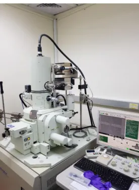
Fig. 2.7 The equipment of EBL process, JEOL JSM7001F.
Table 2.2 E-beam lithography conditions
Pattern Formation Conditions
Spinning and Coating(495PMMA) 3000 rpm 30 sec
Bake 180oC 5min
Spinning and Coating(950PMMA) 3000 rpm 30 sec
Bake 180oC 5min
dosage of electron 200µC/cm2
Development(1:3 MIBK to IPA) 1min
Rinse(IPA) 30sec
2.1.4 Evaporation System
Evaporation is a common method to deposit a thin film onto a substrate. The source material is evaporated in a vacuum. The vacuum allows vapor particles to travel directly to the substrate, where they condense back to a solid state. In this research, metal is deposited by thermal evaporation or e-gun evaporation process under a vacuum of 4*10-6 Torr.
2.1.5 Rapid Thermal Annealing (RTA)
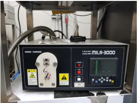
Rapid thermal anneal (RTA) is a subset of Rapid Thermal Processing. It is a process used in semiconductor device fabrication which consists of heating a single wafer for a period of time in order to affect its electrical properties. In this research, the RTA system is MILA-3000.
Fig. 2.8 The equipment of RTA system, MILA-3000
2.1.6 Heterostructure Fabrication System
Heterosutructure fabrication system, which consists of three axis micrometer stage (Fig. 2.9) and optical microscopy, is shown in Fig. 2.10. By using this micromanipulator, BP can be transferred to the desired position of our substrate.
First, after the setup of our system, BP flakes are exfoliated onto the PDMS stamp. Next, the target sample is fixed on the stage (Fig. 2.10) by using double side tape and find the position that we want to fabricate heterostructure. Third, the PDMS stamp is inspected under the optical microscope to select the flake that we want to use.
As the PDMS is transparent, we can see the target sample through it and thus it is possible to align the desired flake on the target sample where we want to transfer the flake with sub-micrometer resolution. Finally, as the desired position is reached, we can lower the glass slide with micromanipulator and let the PDMS stamp be adhered to the target sample to fabricate heterostructue.
Fig. 2.9 Three axis micrometer stage.
Fig. 2.10 Heterosutructure fabrication system.
2.2 Measurement Techniques
2.2.1 Optical Microscopy (OM)
For mechanically exfoliated BP, it's important to find BP flake with appropriate
thickness and size. The film is inspected under the optical microscope and the level of contrast depends on the thickness of the film and the oxide layer. Just in analogy with graphene, the color contrast between BP nanosheets and the underlying SiO2 is due to the interference of different wavelengths through the thin film and SiO2. It means that
optical imaging offers the possibility of simple, rapid and non-destructive characterization of large-area samples [69].
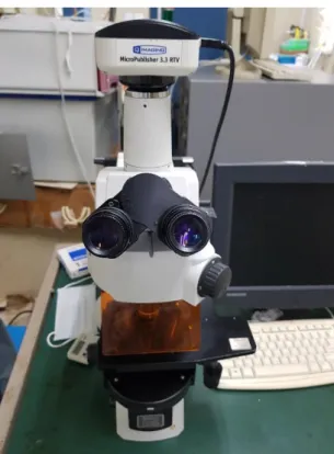
Fig. 2.11 The optical microscopy used in this research.
2.2.2 Atomic Force Microscopy (AFM)
Atomic force microscopy (AFM) is a very high-resolution type of scanning probe microscopy, with demonstrated resolution on the order of a fraction of a nanometer, more than 1000 times better than the optical diffraction limit.
In this research, AFM is used to check the thickness of BP nanosheets by standard tapping mode, which relies on the decreasing of the oscillation amplitude when the tip comes close to the surface.
(a)
(b)
Fig. 2.12 (a) and (b) indicates that the thickness of this BP nanosheet is roughly 15nm.
2.2.3 Raman Spectroscopy
Raman spectroscopy is a spectroscopic technique used to observe vibrational, rotational, and other low-frequency modes in a system. The laser light interacts with molecular vibrations, phonons or other excitations, resulting in the energy of the laser photons being shifted up or down. Therefore, the shift in energy gives information about the vibrational modes in the system.
In this research, 532nm laser is used in Raman measurement. It gives the
Fig. 2.13 The equipment of Raman measurement used in this research.
2.2.4 X-ray Diffraction (XRD)
X-ray crystallography is a technique used for determining the atomic and molecular structure of a crystal, in which the crystalline atoms cause a beam of incident X-rays to diffract into many specific directions. By measuring the angles and intensities of these diffracted beams, a crystallographer can produce a three-dimensional picture of the density of electrons within the crystal. From this electron density, the mean positions of the atoms in the crystal can be determined, as well as their chemical bonds, their disorder, and various other information.
In this research, the wavelength of the X-ray is 1.54Å . The BP bulk is grounded
into powder in order to reduce the non-ideal scattering. The crystal structures of BP
bulk can be determined from XRD measurement.
2.2.5 X-ray Photoelectron Spectroscopy (XPS)
X-ray Photoelectron Spectroscopy (XPS) is a quantitative spectroscopic technique that measures the elemental composition, empirical formula, chemical state and electronic state of the elements that exist in a material. XPS spectra are obtained by irradiating a material with a beam of X-rays while simultaneously measuring the kinetic energy and number of electrons that escape from the top 1 to 10 nm of the material being analyzed.
In XPS, photons with sufficient energy Ephoton are absorbed by a system causing core electrons escaped from the sample. If the energy of the photons is larger than the binding energy of the electron Ebinding, the excess energy will be converted to kinetic energy of the emitted photoelectron, as shown in Fig. 2.14. The binding energy of the core level electron can be calculated according to
Ebinding = Ephoton – ( Ekinetic + φspec )
(2.1)
where Ebinding is the binding energy of the core electron from the Fermi level, Ephoton is the energy of the X-ray photons being used, Ekinetic is the kinetic energy of the electron measured by the instrument and φspec the work function of the spectrometer.
Fig. 2.14 Energy level diagram of the emitted photoelectron.
In this research, Al-Kα (1486.6eV) is used as a X-ray source. The spot size is 400 um and the analysis binding energy values is from 123eV to 143eV. The XPS measurement is used to understand the oxidation rate of BP bulk by measuring the
ratio between the intensity of P2O5 and phosphorus.
2.2.6 Ultraviolet Photoemission Spectroscopy (UPS)
There are two major technique to measure photoemission spectra of atoms, i.e., Ultraviolet photoemission spectroscopy (UPS) and X-ray Photoelectron Spectroscopy
(XPS). The basic theory of the photoemission is illustrated in Fig. 2.15 (a) and (b).
The ultraviolet photons to have lower energies that can be used to study the molecular orbital energies in the valence band region. Through the analysis of escaped
kinetic energy of photoelectrons, the binding energy of the specific molecular orbital energy can be calculated. Besides, the work function at the surface of black phosphorus can be obtained from Eq. (2.2).
( )
binding photon kinetic
E E E (2.2) where Ebinding is the binding energy of the electron, Ephoton is the energy of the UV, Ekinetic is the kinetic energy of the electron and is the work function of the material.
In this research, the fermi level and work function differences before and after oxidation is presented.
(a)
(b)
Fig. 2.15 (a) and (b) Schematic diagram showing how photoelectrons
are generated.
2.2.7 Current – Voltage Characteristics
The current-voltage (I-V) characteristics of the BP thin film transistor were
measured by Agilent B1500A Semiconductor Device Parameter Analyzer. The field effect mobility (μEF) of the TFT can be obtained by the transconductance (gm) with
low VD.
m EF
i D
g C WV
L
(2.2)
where W(L) is the channel width (length), Ci is the capacitance per unit area. VT can also be determined using linear extrapolation of the ID -VG plot.
Chapter 3 Material Analysis for Black Phosphorus
In this chapter, the material analysis for the exfoliated black phosphorus will be
investigated in details.
3.1 Crystal Structure of Black Phosphorus
It is important to confirm the crystalline structure of BP before fabricating a TFT device. By studying its X-ray diffraction pattern, as shown in Fig 3.1(a), the strong diffraction peaks at 16.9°, (002) plane, and 34.2°, (004) plane, were recognized, following the weaker peaks at 26.5°, 40.1°, 52.4°, 56° and 56.7°, corresponding to (012), (014), (006), (105) and (016) planes, respectively. The distance between the atomic planes in the BP bulk can also be calculated from the XRD pattern using the Bragg equation:
2𝑑𝑠𝑖𝑛𝜃 = 𝑛𝜆 (3.1) where d is the distance between the atomic planes, θ is the Bragg scattering angle, n is the diffraction order and λ is the wavelength of incident X-ray. Since the crystalline form of black phosphorus is orthorhombic [70, 71], the reciprocal lattice vectors (hkl) can be obtained from the theoretical lattice constants (abc) and Eq. (3.2):
12 𝑑2 = ℎ2
𝑎2+𝑘2
𝑏2+ 𝑙2
𝑐2 (3.2) After the peaks and their corresponding reciprocal lattice vectors were
determined, the lattice constants can be calculated, as shown in Fig. 3.1 (b) and (c).
The lattice constants for bulk black phosphorus are a = 3.31 Å, b = 4.37 Å, and c = 10.48 Å, corresponding to zigzag, armchair and out of plane directions respectively and are in good agreement with the previous experimental values [30, 72, 73]. The atomic density is 5.26*1022 #/cm3, and the density of bulk BP is 2.7 g/cm3. Because the unit cell contains two layers, the lattice constant c = 10.48 Å indicates that the average interlayer spacing is close to 5.24Å. Therefore, the number of layers for exfoliated BP thin films can be easily determined if the thickness of the BP nanosheets is known.
(a)
(b) (c)
Fig. 3.1 (a) The X-ray diffraction pattern of bulk BP crystal.
Schematic of the unit cell of BP. (b) Top View. (c) Lateral view.
3.2 Characterization of Black Phosphorus Film Thickness
In this section, the BP flakes with appropriate thickness are chosen under optical microscope. After fabrication process and measurement, atomic force microscope is
used to precisely determine the exact layer number of BP nanosheets.
3.2.1 Optical Microscopy (OM)
For mechanically exfoliated BP, it's important to find BP flakes with proper
thickness. The film is scrutinized under the optical microscope while the level of color contrast depends on both the thickness of the film and the underlying oxide layer. The color contrast between BP flakes and the bottom SiO2 is due to the interference of different wavelengths through the thin film and SiO2, just in analogy with graphene, which means that optical imaging is a simple, rapid and non-destructive method to
characterize the thickness of exfoliated BP films [69].
After measuring several BP flakes by AFM, the relationship between the color of BP nanosheets under optical microscope and the thickness of BP thin films is found.
Table 3.1 lists the color of BP flake as a function of its thickness on a 300 nm SiO2/Si substrate. As the thickness decreases, the color changes from red to green as a result of optical interference effects with the oxide. Although the color seems similar when
the BP nanosheet is thinner than 20 nm, the transparency of the flake can be used to
roughly identify the number of layers.
Table 3.1 Thickness dependence of color for BP film on 300 nm SiO
2/Si substrate under optical microscopy.
3.2.2 Atomic Force Microscope (AFM)
According to chapter 3.1, the thickness of a phosphorene layer is 0.52 nm.
Therefore, it is easy to identify the layer number by measuring the thickness of the BP nanosheet. In this research, the standard tapping mode of AFM is used. It provides a more accurate measurement than that of the optical microscope. However, since the process of this measurement is pretty time-consuming, and black phosphorus will gradually degrade due to the long time exposure to ambient atmosphere, the thickness
Thickness Color
<20nm green
20nm~30 nm yellow-green
30nm~60 nm yellow
60nm~80 nm orange
>80nm red
identification by AFM would not be conducted until the other processes had been completed. Fig. 3.2 (a) shows the OM image of an exfoliated BP nanosheet with green color. Fig. 3.2 (b) shows the AFM image of this BP nanosheet. The white line in (b) marks the position of the line profiles shown in Fig. 3.2 (c). The thickness of this BP nanosheet is about 14 nm, which is consistent with Table. 3.1 and implies that the layer number is roughly about 28. Fig. 3.3 (a) shows another exfoliated BP nanosheet with yellow color, and the AFM result of this BP flake is also shown in Fig.
3.3 (b) and (c). Finally, a BP nanosheet with both green and yellow color is shown in Fig. 3.4 (a), and the AFM results of the green and yellow parts of this BP thin film are shown in Fig. 3.4 (b)、(c) and (d)、(e), respectively. These AFM results indicate that
the thickness of an mechanically exfoliated BP nanosheet can be really non-uniform, and the large surface roughness in few-layered phosphorene samples can lead to the measurement error in AFM. Besides, the scanning rate of AFM is slow as compared to the fast degradation rate of few-layered phosphorene in ambient conditions. As a result, the rapid, non-intrusive and accurate method for identifying the thickness of a BP nanosheet is required.
(a)
(b)
(c)
Fig. 3.2 (a) The OM image of an exfoliated BP nanosheet with green color. (b) The AFM image of this BP nanosheet. The white line marks
the position of the line profiles shown in (c). (c) AFM line profile for
20 um
(a)
(b)
(c)
Fig. 3.3 (a) The OM image of an exfoliated BP nanosheet with yellow color. (b) The AFM image of this BP nanosheet. The white line marks the position of the line profiles shown in (c). (c) AFM line profile for the thickness of BP. The thickness of
4 um
(a)
(b)
(c)
(d)
(e)
20 um
Fig. 3.4 (a) The OM image of an exfoliated BP nanosheet with both green and yellow color. (b) and (d) The AFM image of this BP nanosheet. The white line, which is at the green and yellow part of this
BP nanosheet, respectively, marks the position of the line profiles shown in (c) and (e), respectively. (c) and (e) AFM line profile for the thickness of BP. The thickness of the green and yellow part of this BP
nanosheet is about 12.4 nm and 29 nm, respectively.
3.3 Raman Spectroscopy
Raman spectroscopy is a spectroscopic technique used to observe vibrational, rotational, and other low-frequency modes in a material. The system used in this research is a 532nm laser. Since it has been reported that the high power laser-induced heat might damage the lattice structure of BP, a low laser power of 15mW was used to avoid the laser-induced degradation [74].
Unlike in TMDCs semiconductors, where Raman mode frequency has a monotonic dependence on the layer number, the black phosphorus has a non-monotonic dependence owing to the complicated Davydov-related effects [75,
76]. The three characteristic Raman modes, Ag1, B2g and Ag2, can be observed under the typical backscattering configuration, as shown in Fig. 3.5, corresponding to the out-of-plane vibration Ag1 (362cm-1), in-plane vibration along the zigzag B2g (439 cm-1) and armchair Ag2 (467 cm-1), respectively [77].
ACS Nano, 2014, 8 (9), pp 9590–9596
Fig. 3.5 Schematic plot showing the vibration directions of Ag
1, B
2g, and Ag
2modes. The atoms oscillate along the z (out-of-plane), x
(zigzag) and y (armchair) directions, respectively.
The anisotropic behavior of BP is probed by angular dependent Raman spectra [78-85]. The incident light was always polarized along the horizontal direction, as shown in Fig. 3.6 (a). θ is the angle between the zigzag direction of the BP with respect to the polarization direction of the incident beam as indicated in Fig. 3.6. The angle dependent intensities of Ag1, B2g, and Ag2 modes were measured from 0° to 180°, considering the two-fold rotational symmetry of BP along the incident direction
found that the Raman intensities show periodic oscillation as a function of the θ angle. The intensity of Ag1 mode didn’t appear much difference as the sample rotating because the vibration direction was always perpendicular to the polarization direction of the incident light. The Ag2 mode reached its minimum intensity when the rotation angle was at 0° and the maximum intensity arose when the rotation angle was at 90°.
The B2g mode exhibited a 90° period and achieved its maximum intensity at both 40°and 130°, as shown in Fig. 3.6 (b) and Fig. 3.7 [78]. The intensities of the Raman modes are determined by the Raman tensors and the scattering geometry. The Raman tensors of 𝐴𝑔 and 𝐵2𝑔 modes can be expressed as:
R(𝐴𝑔) = (
|𝑎|𝑒𝑖𝜙𝑎 0 0 0 |𝑏|𝑒𝑖𝜙𝑏 0
0 0 |𝑐|𝑒𝑖𝜙𝑐 )
𝑅(𝐵2𝑔) = (
0 0 |𝑓|𝑒𝑖𝜙𝑓 0 0 0
|𝑓|𝑒𝑖𝜙𝑓 0 0 )
where a, b, c and f represent the amplitude of respective vibration modes. Notice that the null components in Raman tensors are due to the symmetry of the BP crystal structure. Considering parallel configuration, the polarization vectors of light can be expressed as:
𝑒̂ = 𝑒𝑖 ̂ = (𝑐𝑜𝑠𝜃 0 𝑠𝑖𝑛𝜃) 𝑠
where the angle θ is measured with respect to the zigzag direction.