Improved n ¿ -GaAs Õ p ¿ -In 0.49 Ga 0.51 P Õ n -GaAs camel-like gate structure for high-breakdown, low-leakage, and high-temperature applications
Wen-Chau Liu,
a)Kuo-Hui Yu, Rong-Chau Liu,
b)Kun-Wei Lin, Chin-Chuan Cheng, Kuan-Po Lin, Chih-Hung Yen, and Cheng-Zu Wu
Institute of Microelectronics, Department of Electrical Engineering, National Cheng-Kung University, 1 University Road, Tainan, Taiwan 70101, Republic of China
共Received 21 February 2001; accepted for publication 26 June 2001兲
A n
⫹-GaAs/ p
⫹-In
0.49Ga
0.51P/n-GaAs camel-like gate structure has been applied to fabricate high-performance transistors. The studied heterostructure field-effect transistor exhibits a large barrier height, high breakdown voltage, low leakage current, and good temperature-dependent characteristics. Experimentally, for a 1 ⫻100 m
2device, the gate-drain breakdown voltage and gate leakage current are 52 共31.5兲 V, and 37 A/mm 共3.5 mA/mm兲 at the gate-drain voltage of 40 V, respectively, at the temperature of 300 共480兲 K. In addition, the high drain-source operation voltage over 20 V with low leakage current is obtained. © 2001 American Institute of Physics.
关DOI: 10.1063/1.1394720兴
High-breakdown voltage is an important factor for het- erostructure field-effect transistors 共HFETs兲 in high-power applications.
1Practically, semiconductor devices operated in high-temperature environment with good performances are needed for automotive, aircraft, space technology, and other applications.
2Therefore, HFETs with remarkable high- breakdown and high-temperature characteristics have been fabricated and reported over the past years. Among them, wide-gap ‘‘insulator,’’ e.g., InGaP and AlGaAs lattice- matched to GaAs substrate or InAlAs and InAlAsSb lattice- matched to InP substrate are frequently used as the Schottky contact layer.
3,4Because the wide-gap insulator offers a large breakdown electric field and high barrier to suppress addi- tional gate leakage current,
3,4the breakdown and temperature characteristics are significantly improved. An alternative method to increase the gate barrier height is the employment of a camel-like diode.
5The advantages of camel-like diode include: 共1兲 alleviation of the problem associated with mak- ing metal–semiconductor contact, 共2兲 easy adjustment of the barrier height, and 共3兲 high reliability under high-power con- ditions. However, the barrier height of a camel-like diode is heavily dependent on the applied gate voltage. As the nega- tive gate bias is increased, the barrier height and breakdown voltage are reduced remarkably. In this work, a p
⫹-In
0.49Ga
0.51P layer is used to replace the conventional p
⫹-GaAs
5to form a heterostructure camel-like gate. The barrier height of the n
⫹-GaAs/ p
⫹-In
0.49Ga
0.51P/n-GaAs camel-like diode is higher than 1.1 eV. This value is higher than the use of insulator layers such as InGaP, AlGaAs, InAlAs, and InAlAsSb with a barrier height of about 0.7–1.0 eV.
3,4The increase of the barrier height induces the decrease of the gate leakage current. Thus, the breakdown and tem- perature characteristics can be improved substantially. In ad- dition, an undoped In
0.15Ga
0.85As channel layer is employed
in the studied device to obtain the good carrier confinement.
Carriers transferring from the inverted delta-doped carrier supply sheet are effectively confined in the In
0.15Ga
0.85As channel.
6Thus, the leakage current is reduced and the break- down voltage can be further improved.
The layer structure was grown by a low-pressure metal- organic chemical vapor deposition system on a 共100兲- oriented semi-insulating GaAs substrate. The epitaxial layers consisted of a 1- m-thick undoped GaAs buffer, a delta- doped sheet 关 ␦ (n
⫹) ⫽4⫻1012 cm
⫺2兴, a 50-Å-thick un- doped GaAs spacer, a 100-Å-thick undoped In
0.15Ga
0.85As channel layer, a 2000-Å-thick GaAs (n ⫽1⫻1017 cm
⫺3), a 100-Å-thick In
0.49Ga
0.51P ( p
⫹⫽8⫻10
18 cm
⫺3), and 300- Å-thick GaAs (n
⫹⫽3⫻10
18 cm
⫺3) cap layers. The growth temperature were 630, 500, and 580 °C for GaAs, InGaAs, and p
⫹-InGaP layer, respectively. During the growth, the pressure was kept at 50 Torr. TMG, TMI, AsH
3, and PH
3
were used as the Ga, In, As, and P source, respectively. SiH
4
and CBr
4 were used as n-type and p-type dopant, respec- tively. After the epitaxial growth, devices were processed by conventional photolithography and vacuum evaporation techniques. The drain-source ohmic contacts were produced on a n-GaAs subchannel layer by alloying evaporated AuGe/Ni metals at 400 °C for 30 s. Then the mesa etching process was used to etch the wafer into the substrate. The ohmic gate was achieved by evaporating Au metals on the n
⫹-GaAs cap layer. Finally, the n
⫹-GaAs and p
⫹-InGaP layers between gate and drain-source electrodes were etched off sequentially. The gate dimension of the studied device is 1 ⫻100 m
2.
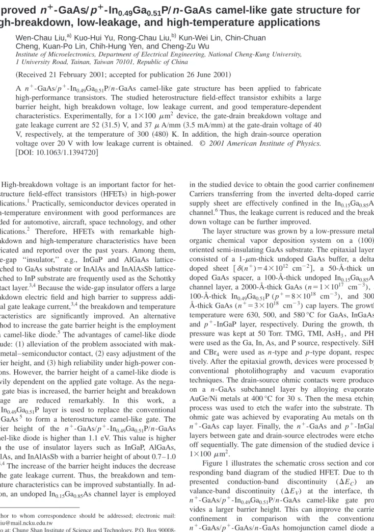
Figure 1 illustrates the schematic cross section and cor- responding band diagram of the studied HFET. Due to the presented conduction-band discontinuity ( ⌬EC) and valance-band discontinuity ( ⌬EV) at the interface, the n
⫹-GaAs/ p
⫹-In
0.49Ga
0.51P/n-GaAs camel-like gate pro- vides a larger barrier height. This can improve the carrier confinement in comparison with the conventional n
⫹-GaAs/ p
⫹-GaAs/n-GaAs homojunction camel diode as depicted by the dashed lines in Fig. 1.
5 The ⌬EC of about
) at the interface, the n
⫹-GaAs/ p
⫹-In
0.49Ga
0.51P/n-GaAs camel-like gate pro- vides a larger barrier height. This can improve the carrier confinement in comparison with the conventional n
⫹-GaAs/ p
⫹-GaAs/n-GaAs homojunction camel diode as depicted by the dashed lines in Fig. 1.
5The ⌬EC of about
a兲Author to whom correspondence should be addressed; electronic mail:
b兲Also at: Chung Shan Institute of Science and Technology, P.O. Box 90008- 9-3, Lung-Tan, Tao-Yuan, Taiwan, Republic of China.
APPLIED PHYSICS LETTERS VOLUME 79, NUMBER 7 13 AUGUST 2001
967
0003-6951/2001/79(7)/967/3/$18.00 © 2001 American Institute of Physics
Downloaded 02 Sep 2008 to 140.116.208.41. Redistribution subject to AIP license or copyright; see http://apl.aip.org/apl/copyright.jsp
200 meV
7at p
⫹-In
0.49Ga
0.51P/n-GaAs interface can effec- tively confine electrons in the channel and the ⌬EVof about 300 meV
7can prevent holes, generated by impact ionization at high drain-source voltage,
8injecting toward the gate elec- trode. Thus, the leakage current and breakdown voltage can be improved. In addition, when carriers transfer from the inverted delta-doped sheet to the In
0.15Ga
0.85As channel, good performances of electron mobility and carrier confine- ment may be expected and the leakage current is then further decreased.
6
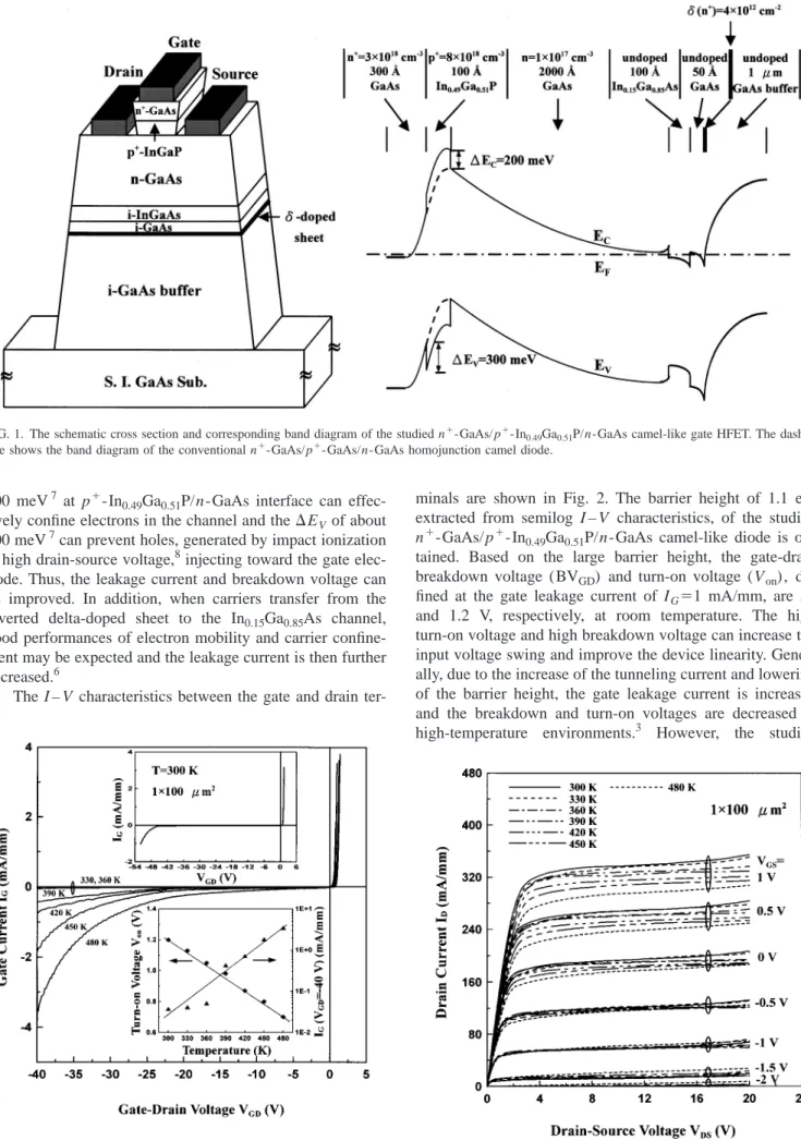
The I – V characteristics between the gate and drain ter-
minals are shown in Fig. 2. The barrier height of 1.1 eV, extracted from semilog I – V characteristics, of the studied n
⫹-GaAs/ p
⫹-In
0.49Ga
0.51P/n-GaAs camel-like diode is ob- tained. Based on the large barrier height, the gate-drain breakdown voltage (BV
GD) and turn-on voltage (V
on), de- fined at the gate leakage current of I
G⫽1 mA/mm, are 52 and 1.2 V, respectively, at room temperature. The high turn-on voltage and high breakdown voltage can increase the input voltage swing and improve the device linearity. Gener- ally, due to the increase of the tunneling current and lowering of the barrier height, the gate leakage current is increased and the breakdown and turn-on voltages are decreased at high-temperature environments.3 However, the studied
FIG. 1. The schematic cross section and corresponding band diagram of the studied n⫹-GaAs/ p⫹-In0.49Ga0.51P/n-GaAs camel-like gate HFET. The dashed line shows the band diagram of the conventional n⫹-GaAs/ p⫹-GaAs/n-GaAs homojunction camel diode.
FIG. 2. Two-terminal gate-drain I – V characteristics of the studied high- barrier camel-like HFET with a gate dimension of 1⫻100m2at different temperatures.
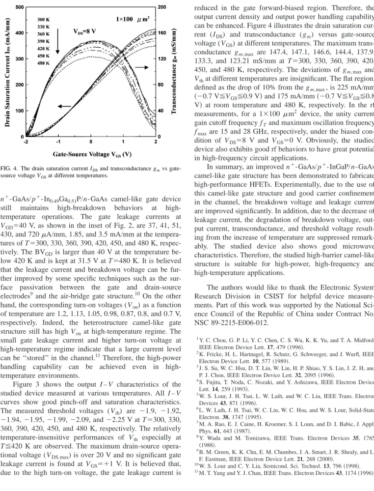
FIG. 3. Source-ground output I – V characteristics of the studied camel-like gate HFET at different temperatures.
968 Appl. Phys. Lett., Vol. 79, No. 7, 13 August 2001 Liuet al.
Downloaded 02 Sep 2008 to 140.116.208.41. Redistribution subject to AIP license or copyright; see http://apl.aip.org/apl/copyright.jsp
n
⫹-GaAs/ p
⫹-In
0.49Ga
0.51P/n-GaAs camel-like gate device still maintains high-breakdown behaviors at high- temperature operations. The gate leakage currents at V
GD⫽40 V, as shown in the inset of Fig. 2, are 37, 41, 51, 430, and 720 A/mm, 1.85, and 3.5 mA/mm at the tempera- tures of T ⫽300, 330, 360, 390, 420, 450, and 480 K, respec- tively. The BVGD is larger than 40 V at the temperature be- low 420 K and is kept at 31.5 V at T ⫽480 K. It is believed that the leakage current and breakdown voltage can be fur- ther improved by some specific techniques such as the sur- face passivation between the gate and drain-source electrodes
9 and the air-bridge gate structure.
10 On the other hand, the corresponding turn-on voltages (V
on) as a function of temperature are 1.2, 1.13, 1.05, 0.98, 0.87, 0.8, and 0.7 V, respectively. Indeed, the heterostructure camel-like gate structure still has high V
on at high-temperature regime. The small gate leakage current and higher turn-on voltage at high-temperature regime indicate that a large current level can be ‘‘stored’’ in the channel.
11Therefore, the high-power handling capability can be achieved even in high- temperature environments.
Figure 3 shows the output I – V characteristics of the studied device measured at various temperatures. All I – V curves show good pinch-off and saturation characteristics.
The measured threshold voltages (V
th) are ⫺1.9, ⫺1.92,
⫺1.94, ⫺1.95, ⫺1.99, ⫺2.09, and ⫺2.25 V at T⫽300, 330, 360, 390, 420, 450, and 480 K, respectively. The relatively temperature-insensitive performances of Vth especially at T ⬉420 K are observed. The maximum drain-source opera- tional voltage (V
DS,max) is over 20 V and no significant gate leakage current is found at V
GS⫽⫹1 V. It is believed that, due to the high turn-on voltage, the gate leakage current is
reduced in the gate forward-biased region. Therefore, the output current density and output power handling capability can be enhanced. Figure 4 illustrates the drain saturation cur- rent (I
DS) and transconductance (g
m) versus gate-source voltage (V
GS) at different temperatures. The maximum trans- conductance g
m,maxare 147.4, 147.1, 146.6, 144.4, 137.9, 133.3, and 123.21 mS/mm at T ⫽300, 330, 360, 390, 420, 450, and 480 K, respectively. The deviations of g
m,maxand V
that different temperatures are insignificant. The flat region, defined as the drop of 10% from the g
m,max, is 225 mA/mm 共⫺0.7 V⬉VGS⬉0.9 V兲 and 175 mA/mm 共⫺0.7 V⬉V
GS⬉0.8 V 兲 at room temperature and 480 K, respectively. In the rf measurements, for a 1 ⫻100 m
2 device, the unity current gain cutoff frequency f
Tand maximum oscillation frequency f
maxare 15 and 28 GHz, respectively, under the biased con- dition of V
DS⫽8 V and V
GS⫽0 V. Obviously, the studied device also exhibits good rf behaviors to have great potential in high-frequency circuit applications.
In summary, an improved n
⫹-GaAs/ p
⫹-InGaP/n-GaAs camel-like gate structure has been demonstrated to fabricate high-performance HFETs. Experimentally, due to the use of this camel-like gate structure and good carrier confinement in the channel, the breakdown voltage and leakage current are improved significantly. In addition, due to the decrease of leakage current, the degradation of breakdown voltage, out- put current, transconductance, and threshold voltage result- ing from the increase of temperature are suppressed remark- ably. The studied device also shows good microwave characteristics. Therefore, the studied high-barrier camel-like structure is suitable for high-power, high-frequency and high-temperature applications.
The authors would like to thank the Electronic System Research Division in CSIST for helpful device measure- ments. Part of this work was supported by the National Sci- ence Council of the Republic of China under Contract No.
NSC 89-2215-E006-012.
1Y. C. Chou, G. P. Li, Y. C. Chen, C. S. Wu, K. K. Yu, and T. A. Midford, IEEE Electron Device Lett. 17, 479
共1996兲.
2K. Fricke, H. L. Hartnagel, R. Schutz, G. Schweeger, and J. Wurfl, IEEE Electron Device Lett. 10, 577
共1989兲.
3J. S. Su, W. C. Hsu, D. T. Lin, W. Lin, H. P. Shiao, Y. S. Lin, J. Z. H, and P. J. Chou, IEEE Electron Device Lett. 32, 2095
共1996兲.
4S. Fujita, T. Noda, C. Nozaki, and Y. Ashizawa, IEEE Electron Device Lett. 14, 259
共1993兲.
5W. S. Lour, J. H. Tsai, L. W. Laih, and W. C. Liu, IEEE Trans. Electron Devices 43, 871
共1996兲.
6L. W. Laih, J. H. Tsai, W. C. Liu, W. C. Hsu, and W. S. Lour, Solid-State Electron. 38, 1747
共1995兲.
7M. A. Rao, E. J. Caine, H. Kroemer, S. I. Loun, and D. I. Babic, J. Appl.
Phys. 61, 643
共1987兲.
8Y. Wada and M. Tomizawa, IEEE Trans. Electron Devices 35, 1765
共1988兲.
9B. M. Green, K. K. Chu, E. M. Chumbes, J. A. Smart, J. R. Shealy, and L.
F. Eastman, IEEE Electron Device Lett. 21, 268
共2000兲.
10W. S. Lour and C. Y. Lia, Semicond. Sci. Technol. 13, 796
共1998兲.
11M. T. Yang and Y. J. Chan, IEEE Trans. Electron Devices 43, 1174
共1996兲.
FIG. 4. The drain saturation current IDSand transconductance gmvs gate- source voltage VGSat different temperatures.
969
Appl. Phys. Lett., Vol. 79, No. 7, 13 August 2001 Liuet al.
Downloaded 02 Sep 2008 to 140.116.208.41. Redistribution subject to AIP license or copyright; see http://apl.aip.org/apl/copyright.jsp