行政院國家科學委員會專題研究計畫 成果報告
奈米金氧半場效電晶體高頻雜訊模擬研究
計畫類別: 個別型計畫
計畫編號: NSC92-2215-E-011-003-
執行期間: 92 年 08 月 01 日至 93 年 07 月 31 日 執行單位: 國立臺灣科技大學電子工程系
計畫主持人: 張勝良
報告類型: 精簡報告
處理方式: 本計畫可公開查詢
中 華 民 國 93 年 7 月 29 日
行政院國家科學委員會專題研究計畫成果報告
奈米金氧半場效電晶體高頻雜訊模擬研究
計畫編號: NSC 92-2215-E-011 -003 – 執行期限:92 年 08 月 01 日至 93 年 07 月 31 日
主持人:張勝良 執行機構及單位名稱 台灣科技大學
一、中文摘要
這個計畫的目的是研究奈米金氧半場效電 晶體的高頻雜訊特性及模型。奈米極金氧 半場效電晶體具有不同於傳統元件之物裡
,本計畫考慮這些元件物理,發展次臨限 區也能適用的熱雜訊模型及閘極感應雜訊 模型。本模型的正確經由實驗得到驗證。
關鍵詞:奈米金氧半場效電晶體,高頻雜 訊,熱雜訊,閘極感應雜訊,次臨限區。
Abstract: At high frequency, the MOSFET drain current noise is generally accepted as dominated by the thermal noise as the MOSFET is operating in strong inversion region. However, controversy exists about the high-frequency noise in subthreshold region. This project proposes a unified high-frequency drain current noise and induced gate noise valid in strong inversion, moderate and weak inversion regions. These models are helpful for low-frequency amplifier design with nanometer technologies with MOSFETs operating in moderate inversion region.
Keywords: high-frequency noise, nanometer MOSFETs, thermal noise, induced gate noise, subthreshold region.
二、緣由與目的
The aggressive scaling of CMOS technologies that has been going on for more than 2 decades has allowed an increase in the number of transistors per chips. The technologies can also be exploited for analog RF circuits, in which good noise performance and low-power consumption are required.
Since the noise figure is also decreasing when increasing the transit frequency [1], it also takes advantage of the down-scaling of the transistor length. The power consumption
is still larger than what you would get from bipolar implementation, but this is changing thanks to scaling. The operating points are moving from strong inversion toward weak inversion, improving the current efficiency and making it closer to what is obtained with a bipolar transistor. Transistors operating in weak inversion exhibit a flat part in the power spectral density for the noise current, just as devices in strong inversion do [2]. In some treatments, this is regarded as caused by thermal noise, just as in strong inversion.
In some other treatments, this is caused by shot noise, which is associated with carriers crossing a potential barrier. The same result is obtained with either of the above two approaches [2] for long-channel devices. To design CMOS LNAs, the authors in [3] use for the drain noise a smooth exponential expression to connect the shot and thermal noise as the gate-to-source voltage increases from below the threshold voltage to the above threshold voltage, which is fully thermal noise when gate drive is much higher than the thermal voltage
V
t and fully shot noise when it is lower than Vt. Pascht et al.[4] proposed a noise model using only a strong-inversion thermal noise model, which is not correct in describing the noise behavior in whole operation region. Obrecht et al.[5]
argued that for long channel devices, thermal noise was confirmed to be the main source of noise in accord with the conventional theory.
In contrast, for submicron devices the shot noise appeared to be dominant. The shot noise component is primarily produced near the source of the device and is believed to be caused by the diffusion current. The purpose of this project is to clarify the controversy about the origin of subthreshold-region high frequency noise in order to have an accurate
noise model for RF circuit design.
三、結果與討論
We have developed the theory for exploring the noise model for nanometer MOSFETs,
the interested reader can refer to ref. [6].
Figure 1 shows the result of long-channel and short-channel MOSFETs biased in the strong region,
S gradually
id decreases withV
DS . In this region the conventional thermal noise derived from drift current equation is applicable. Simulation was conducted for devices with dimension of W/L = 96µ
m/5.25µ
m and 96µ
m/0.18µ
m.For a long channel MOSFET,
S may have
id a reduction of factor about six. But for a short channel MOSFET the factor of reduction is much greater, it accounts for the non-saturation effect of theI
DS− V
DS curve;the MOSFET more suffers the affection of thermal noise increment for short channel than long channel especially in the linear region. It has an easy way to get the physical behavior of the thermal noise. Since the general form of thermal noise is
S
id=
4kTg
d, and a MOSFET can be thought as a modulated conductance, the output conductanceg has a higher value in the
d linear region than in the saturation region.However the variations of
g
d cannot explain the increasingS
id whenV
DS approaches to 0 V. According to theory equation (18) in [6] , it provides a betterunderstanding that occurs because the inversion areal charge density
Q
inv at the drain increases when the operation point is translated from the saturation region to the linear region.Figure 2 shows the result of a MOSFEET biased in the weak inversion region,
S
id also decreases withV
DS . Simulation was conducted for a device with a dimension of W/L = 96µ
m/5.25µ
m and W/L = 96µ
m/0.18µ
m. It occurs because the inversion areal charge density at the drain decreases when the operation point is translated from the linear region to the saturation region. For a long channel MOSFET,S may have reduction of factor
id two [7]. But for a short channel MOSFET the factor of reduction is higher, it accounts for the non-saturation effect, and the drain saturation currentI
DSAT cannot be defined exactly. Secondly, since drain current is dominated by diffusion current in weak inversion region,S
id cannot be derived directly from the drift model equation (3) in [6] with the dynamic conductance given by0 0 0 0
( ) OX( GS T ) /[1 ( GS T )]
g V = µ WC V − − V V + θ V − − V V
. We should use the effective dynamic conductance given by equation (20) in [6].Ghibaudo and Boutchacha [8] used the thermal noise model derived from strong-inversion model to predict the thermal noise in weak inversion; their result also shows this trend. But the physical meaning of
their equation has a flaw; why the result derived form drift equation can be applied to describe a physical phenomena sue to the diffusion mechanism. Besides the
g
d( )φ
c used in their equation is expressed as a function quasi-Fermi potential shift, which has not been derived before. In our model, the effectiveg V
( 0) is valid in whole operation region; the results can be used to calculate the thermal noise both in the weak and strong inversion regions. Although the two forms of shot and thermal noise can even be identical [7], whereas it doesn’t for short-channel or strong inversion.Figure 3 shows the comparison of the strong inversion model,
S
ig strong, with exponential term, and the measured data [9] of MOSFETs with dimensions of W/L = 60 µm / 0.64, 0.42, 0.18 µm and biased atV
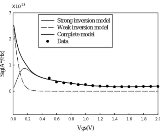
DS = 1.0 V. We find it has a well agreement.Figure 4 shows the comparison of the complete model of equation (26) in [6] and the measured data [9] of a MOSFET with dimension of W / L = 60 µm / 0.42 µm and biased at
V
DS = 1.0 V. The dashed line is, ig weak
S
with multiplying exponential term, the solid line isS
ig strong, with multiplying exponential term, and the thick solid line is the sum of the previous two. We find in the weak inversion regionS
ig is dominated by, ig weak
S
and reaches a maximum value whenV
GS approaches to 0 V. With the increasing ofV
GS, theS
ig strong, takes over the dominant and agrees with the measured data. Equation (26) in [6] can well describe the variation between the strong and weak inversion regions.四、圖表
0 .0 0.1 0 .2 0 .3 0 .4 0 .5
Sid (A2/Hz) 0.0 2.0 e -2 2 4.0 e -2 2 6.0 e -2 2 8.0 e -2 2 1.0 e -2 1 1.2 e -2 1 1.4 e -2 1 1.6 e -2 1 1.8 e -2 1
W /L = 9 6 u m /0 .18 u m
Vd s (V )
0.0 0 .1 0 .2 0 .3 0 .4 0.5
Sid (A2/Hz)
0 1 e -2 4 2 e -2 4 3 e -2 4 4 e -2 4 5 e -2 4 6 e -2 4 7 e -2 4
W /L = 9 6 u m /2 .25 u m
F ig . 1 . T he rm a l n o ise Sid v e rsu s Vd s fo r M O S F E T s bia s e d in stro n g in v ers io n re g io n.
0 .0 0 .1 0 .2 0 .3 0 .4 0 .5
Sid ( A2/Hz ) 0 2 e -2 2 4 e -2 2 6 e -2 2 8 e -2 2
W /L = 9 6 u m /0 .1 8 u m
V d s (V )
0 .0 0 .1 0 .2 0 .3 0 .4 0 .5
Sid ( A2/Hz )
1 .0 e -2 4 1 .2 e -2 4 1 .4 e -2 4 1 .6 e -2 4 1 .8 e -2 4 2 .0 e -2 4 2 .2 e -2 4 2 .4 e -2 4
W /L = 9 6 u m /2 .2 5 u m
F ig . 2 . T h e rm a l n o is e S id v e rsu s V d s fo r M O S F E T s b ia se d in w e a k in v e rs io n re g io n .
V g s ( V )
0 .0 0 .2 0 .4 0 .6 0 .8 1 .0 1 .2 1 .4 1 .6 1 .8 2 .0
Sig(A2/Hz)
0 .0 1 0 .1 0 1 .0 0
X 1 0- 2 3
L = 0 .1 8 u m L = 0 .4 2 u m
L = 0 .6 4 u m
F ig . 3 . C o m p a r is o n o f s im u la tio n a n d m e a s u r e d a ta fo r M O S F E T s b ia s e d a t Vd s = 1 .0 V w ith W / L = 6 0 u m / 0 .6 4 u m , 0 .4 2 u m , 0 .1 8 u m .
Vgs(V)
0.0 0.2 0.4 0.6 0.8 1.0 1.2 1.4 1.6 1.8 2.0
Sig(A2/Hz)
0 1 2 3
Strong inversion model Weak inversion model Complete model Data X10-23
Fig. 4. Illustration of the variation of the strong, weak and complate models.
五、參考文獻
[l] C. Enz, ”An MOS transistor model for RF IC design valid in all regions of operation,” IEEE Trans. Microwave Theory and tech., Vol. 50, N0. 1, pp. 342, 2002.
[2] Y. Tsividis, Operation and Modeling of the MOS Transistor, 2nd ed. New York: McGraw-Hill, 1999.
[3] F. Gatta, E. Sacchi, F. Svelto, P. Vilmercati, and R. Castello, “A 2-dB Noise figure 900-MHz differential CMOS LNA,” IEEE J.
Solid-State Circuits, vol. 36, pp. 1444–1452, 2001.
[4] A. Pascht, M. Grözing, D. Wiegner, and M. Berroth,”
Small-signal and temperature noise model for MOSFETs,” IEEE Trans. Microwave Theory and Tech., Vol. 50, No. 8, pp.1927-1933, 2002
[5] M. S. Obrecht, E. Abou-Allam, and T. Manku, ”Diffusion current and its effect on noise in submicron MOSFETs,” IEEE Trans. Electron Devices, Vol. 49, No. 3, pp.524-526, 2002.
[6] H. F.. Teng, S. L. Jang, and M. H. Juang, ” A unified model for high-frequency drain current noise of MOSFETs,” Solid-state Electronics, Vol. 47, pp.2043-2048, 2003.
[7] R. Sarpeshkar, T. Delbruck, and C. A. Mead,” White noise in MOS transistors and resistors,” Circuits and Devices, Vol. 9, No. 6, pp.23-29, 1993.
[8] G. Ghibaudo, T. Boutchacha “ Electical noise and RTS fluctuations in advanced CMOS devices “Microelectronics Reliability, Vol. 42, pp. 573-582, 2002.
[9] Chih-Hung Chen, Deen M. J., Yuhua Cheng, Matloubian. M.,”
Extraction of the induced gate noise, channel noise, and their correlation in submicron MOSFETs from RF noise measurements”
IEEE Trans, Electron Devices, Vol. 48, No. 12, Dec 2001, pp.2884 –2892.
![Figure 3 shows the comparison of the strong inversion model, S ig strong, with exponential term, and the measured data [9] of MOSFETs with dimensions of W/L = 60 µm / 0.64, 0.42, 0.18 µm and biased at V DS = 1.0 V](https://thumb-ap.123doks.com/thumbv2/9libinfo/9127301.411505/4.892.468.799.99.876/figure-comparison-strong-inversion-exponential-measured-mosfets-dimensions.webp)