A Sn-based metal substrate technology for the fabrication
of vertical-structured GaN-based light-emitting diodes
Hon-Yi Kuo, Shui-Jinn Wang,a兲 and Pei-Ren Wang
Institute of Microelectronics, Department of Electrical Engineering, National Cheng Kung University, Tainan 701, Taiwan, Republic of China
Kai-Ming Uang and Tron-Min Chen
Department of Electrical Engineering, Wu Feng Institute of Technology, Chiayi 621, Taiwan, Republic of China
Hon Kuan
Optoelectronics Center of Far East University, Tainan 744, Taiwan, Republic of China
共Received 1 October 2007; accepted 17 December 2007; published online 14 January 2008兲 Through the use of tin共Sn兲 based solder balls and patterned laser lift-off technique, a metal substrate technology was proposed for the fabrication of vertical-structured metal substrate GaN-based light-emitting diodes 共VM-LEDs兲. Advantages including reserving the merits of metallic substrate and simplifying the fabrication processes of vertical-structured GaN-based LEDs were demonstrated. As compared to conventional sapphire substrate GaN-based LEDs, the fabricated VM-LEDs with an emission area of 620⫻620m2show an increase in light output power about
145.36% at 350 mA with a significant decrease in forward voltage from 4.51 to 3.46 V. © 2008 American Institute of Physics. 关DOI:10.1063/1.2834373兴
Recently, continuous efforts have been made to develop high power and high efficiency white light GaN-based light-emitting diodes 共LEDs兲 for the applications of flashlight, backlight source for liquid crystal display, and even solid-state lighting.1,2 To solve the severe current-crowding effect and heat accumulation issues due to insulating sapphire sub-strate used in conventional p-side up GaN-based LEDs 共namely, regular LEDs兲, substrate transfer techniques by means of laser lift-off共LLO兲 with wafer bonding or electro-plating have been reported for the fabrication of vertical-structured GaN-based LEDs.2–5 Lately, the author’s groups demonstrated the use of selective electroplating nickel 共Ni兲 substrates with patterned LLO for the fabrication of vertical-structured metal-substrate GaN-based light-emitting diodes 共VM-LEDs兲.4
Advantages including avoidance of metal cut-ting and better electrical and optical characteristics in com-parison with regular LEDs have been presented.
To package high performance LED chips, tin-based sol-der materials have been widely adopted as a substitute for conventional epoxy or conductive glue used in the die-attaching process for its superior thermal and electrical char-acteristics. In this paper, to simplify the device fabrication processes of VM-LEDs with high throughput, cost effective-ness, and environmental friendlieffective-ness, a metal substrate tech-nology using tin共Sn兲 based solder balls with a nickel barrier layer and a Au wetting layer was proposed and demon-strated. Electrical and optical characteristics of the fabricated VM-LEDs were reported and compared to those of regular LEDs as well.
Figures 1共a兲 and 1共b兲 illustrate schematically the layer structure and key fabrication processes of the VM-LEDs us-ing the proposed metal substrate engineerus-ing. Here, lead-free Sn-based 共a Sn–Ag–Cu–Au alloy兲 solder balls were em-ployed for the implementation of dicing free metal
sub-strates. The samples prepared in this work were epitaxially grown on sapphire substrate by metal-organic chemical va-por deposition. For the details of the layer structure, please refer to Ref.6. Note that oxidized Ni共2.5 nm兲/Au共3.5 nm兲, Ti共15 nm兲/Al共400 nm兲/Ti共100 nm兲/Au共200 nm兲, and Ni共200 nm兲Au共200 nm兲 metal systems were deposited se-quentially on p-GaN layer by e-beam evaporator to serve as Ohmic contact, adhesive/mirror layer, and barrier/wetting layer, respectively.
To pursue dicing free, a photolithography process using thick SU8-2035 photoresist was employed to defined the de-vice region 共750⫻750m2兲 with a cutting-way width of 90m, followed by a selective electroplating process to form 10-m-thick Ni metal frames over the entire cutting-way region under a constant current of 1.7 A for 10 min. After that, Sn-based solder balls共350m in diameter兲 were placed within each device region and a rapid-thermal 共RT兲 reflow treatment at 280– 300 ° C for 90 s was conducted. Note the increasing rate of temperature was kept at 1.7 ° C/s. After that, the samples were cooled at a rate of −0.5 ° C/s and the patterned Sn-based metal substrates formed. It should be mentioned here that the melting point, reflow tem-perature, and thermal conductivity of the Sn-based substrate could be increased via a suitable change in its alloy compo-sition to accommodate surface mount technology used for LED applications.7 Note that the Ni metal frames which acted as molds to confine melting Sn-based alloy during the RT reflow process were autolifted after the RT reflow treat-ment because of the difference in thermal expansion coeffi-cient with respect to the beneath metal layers.
Prior to the patterned LLO process, the sample was glued to a temporal silicon 共Si兲 substrate with polyamide. Through the use of a mask to define both size 共620 ⫻620m2兲 and shape of excimer laser beam 共248 nm兲 and
an alignment to the patterned Sn-based metal substrate, the patterned LLO process关Fig.1共a兲兴 was performed at a
reac-a兲Electronic mail: [email protected].
APPLIED PHYSICS LETTERS 92, 021105共2008兲
0003-6951/2008/92共2兲/021105/3/$23.00 92, 021105-1 © 2008 American Institute of Physics
tive energy of 850 mJ/cm2.4,6
It should be noted that the area ratio of the laser beam size共also the size of the device emis-sion area兲 to the chip size 共i.e., device region兲 was kept to be less than 1共0.82 in the present work兲 to prevent the edge of epitaxial structure from irregular breach or flaw during the fabrication of device.4The sample was then heated to about 40 ° C for 10 min to remove the sapphire substrate.
To remove the u-GaN, an inductively coupled plasma dry-etching process was conducted. For better light extrac-tion and the contact characteristics, a surface treatment with 6 mol KOH solution at 60 ° C for 90 s was also made.6After the surface of the exposed n-GaN was cleaned with HF and diluted HCl: H2O 共1:1兲 solution for 1 min, a metal contact
pad comprised of Ti–Al–Ti–Au was deposited by e-beam evaporator关Fig.1共b兲兴. Finally, the temporal silicon substrate was replaced with a blue tape and the fabrication of the pro-posed n-side up VM-LED chips with Sn-based metal sub-strates was completed. Note that regular LEDs, as shown in Fig.1共c兲, of the same chip size with two electrodes on the same side of the device were also fabricated with the same wafer for comparison.
Figure 2共a兲 shows that top view of the oval-like pat-terned Sn-based metal substrate due to its cohesion. Figure 2共b兲shows the cross-sectional structure of the sample before patterned LLO. Flat and smooth interface between GaN ep-ilayer and metal layers was observed. By energy dispersive x-ray spectrum analysis 共not shown兲, Ni/Au layer was proved to effectively prevent Sn from reacting with the
struc-ture underneath during the reflow process. Figure2共c兲shows the top view of the exposed n-GaN. An even GaN surface was obtained. Figure2共d兲 reveals that the Ni metal frames were completely self-removed after the RT reflow treatment. The comparison of current-voltage 共I-V兲 characteristics of the fabricated VM-LEDs and regular LEDs with the same chip size were shown in Fig.3. It is seen that, at an injection current of 350 mA, the forward voltage共VF兲 of the proposed VM-LEDs are 3.46 V, which is comparably good with pre-vious works reported by Chen et al.4and Lin et al.5in spite of the smaller chip size, while that of the regular one is 4.51 V. As compared with regular LEDs, the reduction in VF of the n-side up VM-LEDs should be attributed to the con-FIG. 1.共Color online兲 The schematic device structure of VM-LEDs using
the proposed Sn-based metal substrate technology at some specific process-ing stages.共a兲 Sample at the patterned LLO processing stage. 共b兲 Sample at the n-GaN Ohmic contact processing stage.共c兲 The schematic cross section of a regular GaN-based LED. Note that device structures shown in the present figure were not in scale.
FIG. 2. 共Color online兲 Scanning electron microscope 共SEM兲 and optical microscope共OM兲 images of samples at some processing states. 共a兲 Top view of the patterned Sn-based metal substrate before the removal of nickel metal frames.共b兲 SEM image of the cross-sectional structure of the sample after the reflow process.共c兲 Top view of the exposed epi-GaN layers after pat-terned LLO process.共d兲 OM image of the exposed n-GaN after the autore-moval of the nickel metal frames.
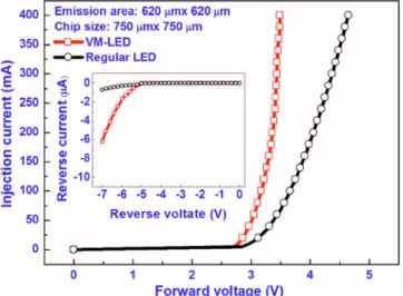
FIG. 3.共Color online兲 Comparison of typical forward current-voltage 共I-V兲 characteristics of VM-LEDs and regular LEDs. The inset shows the reverse current characteristic of VM and regular LEDs
021105-2 Kuo et al. Appl. Phys. Lett. 92, 021105共2008兲
siderable improvement in current spreading and the realiza-tion of a much shorter vertical conducrealiza-tion path between the two electrodes共⬃4m in this work兲.4–6 It is noted that the incremental series resistance关共i/v兲−1兴 of the VM-LEDs is
about 1.0⍀ at 350 mA, which is about 1/3 that of regular LEDs at the same current. The inset of Fig. 3 shows the typical reverse characteristics of VM and regular LEDs. It is seen that the VM-LED has a relatively inferior reverse char-acteristic. This might be attributed to the LLO process that increases the density of screw dislocations, which penetrated through the MQW region, and/or causes damages to the pe-riphery of the device.8 Optimization of the LLO process to minimize the damage to the epilayer and utilization of suit-able passivation to VM-LEDs are now underway.
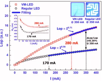
Figure 4 shows the typical light output power–current 共Lop-I兲 characteristics of VM-LEDs and regular LEDs. The
proposed VM-LED was found having an increase in light output power共i.e., ⌬Lop/Lop兲 of about 145.36% over that of
regular LEDs at 350 mA. The power conversion efficiency 共= Po/ Pe, i.e., the ratio of optical output power Po to input electrical power Pe兲 of the VM-LEDs at 350 mA is about 3.20⫻ of that of regular LEDs. These improvements should be mainly attributed to the fact that the vertical structure itself provides better current spreading, less series resistance, larger light extraction area benefiting from single electrode on top n-GaN, surface roughening on n-GaN layer, and higher light reflection.4 Through curve fitting for both the Lop-I curves at high injection currents 共blue solid lines兲, it
was found that the dependence of light output power of the VM and regular LED on the injection current can be ex-pressed as Lop⬀I0.71 and Lop⬀I0.56, respectively. As we
ex-pected, the light output power of the VM-LED exhibited a better response under high injection currents. Note that the
improvement in ⌬Lop/Lop and are comparably good with
previous works, indicating that the present Sn-based sub-strate technology would be attractive for thin GaN LED fabrication.4,5
The dependence of peak wavelength 共WP兲 on injection current of both VM and regular LEDs was also plotted in the inset of Fig.4. Under low injection currents, the band-filling effects dominated and led to the blueshift in WP for both the VM and regular LEDs.9–11As the injection current was fur-ther increased, accumulation of Joule heating attributed to series resistance and nonradiative recombination of carriers results in a strong redshift and the blueshift from the band filling effect was overridden.10One observes that the prevail-ing of the redshift occurred at 170 and 280 mA for the regu-lar and VM-LEDs, respectively. It reveals that a relatively slight accumulation of Joule heating of the VM-LEDs was achieved.
In summary, a metal substrate technology using Sn-based solder balls and patterned laser LLO technique for the fabrication of VM-LEDs has been proposed and stimulating experimental results have been demonstrated. As compared to regular LEDs, the proposed VM-LEDs have been shown to have an enhancement in Lopabout 145.36% and a VFdrop of 1.05 V at 350 mA, which provides an improvement in the power conversion efficiency by about 3.20⫻ that of regular LEDs. It is expected that the proposed Sn-based metal sub-strate technology would be a potential candidate for the fab-rication of high power GaN-based LEDs for solid-state light-ing in the near future.
This work was supported by the National Science Coun-cil共NSC兲 of Taiwan, Republic of China, under Contract No. NSC 95-2215-E-006-014 and the Landmark Project Grant for NCKU’s Top-University Project.
1J. J. Wierer, D. A. Steigerwald, M. R. Krames, J. J. O’Shea, M. J.
Ludo-wise, G. Christenson, Y. C. Shen, C. Lowery, P. S. Martin, S. Subramanya, W. Gotz, N. F. Gardner, R. S. Kern, and S. A. Stockman, Appl. Phys. Lett.
78, 3379共2001兲.
2W. S. Wong and T. Sands, Appl. Phys. Lett. 75, 1360共1999兲.
3T. Fujji, Y. Gao, R. Sharma, E. L. Hu, S. P. DenBaars, and S. Nakamura,
Appl. Phys. Lett. 84, 855共2004兲.
4S. L. Chen, S. J. Wang, K. M. Uang, T. M. Chen, W. C. Lee, and B. W.
Liou, IEEE Photonics Technol. Lett. 19, 351共2007兲.
5W. Y. Lin, D. S. Wuu, K. F. Pan, S. H. Hung, C. E. Lee, W. K. Wang, S.
C. Hsu, Y. Y. Su, S. Y. Huang, and R. H. Horng, IEEE Photonics Technol. Lett. 17, 1809共2005兲.
6K. M. Uang, S. J. Wang, S. L. Chen, Y. C. Yang, T. M. Chen, and B. W.
Liou, Jpn. J. Appl. Phys., Part 1 45, 3436共2006兲.
7G. Elger, M. Hutter, H. Oppermann, R. Aschenbrenner, H. Reichl, and E.
Jäger, Microsyst. Technol. 7, 239共2002兲.
8Y. S. Wu, J. H. Chen, and W. C. Peng, Appl. Phys. Lett. 90, 251110
共2007兲.
9Y. Li, W. Fang, W. Liu, H. Liu, C. Mo, L. Wang, and F. Jiang, J. Lumin. 122-123, 567共2007兲.
10T. Mukai, M. Yamada, and S. Nakamura, Jpn. J. Appl. Phys., Part 2 11B,
L1358共1998兲.
11T. Kuroda, A. Tackeuchi, and T. Sota, Appl. Phys. Lett. 76, 3753共2000兲.
FIG. 4. 共Color online兲 Comparison of typical Lop-I characteristics of
VM-LEDs and regular LEDs. The inset shows the comparison of the peak wavelength dependence on injection current and light emission images at 350 mA of the VM and regular LED.
021105-3 Kuo et al. Appl. Phys. Lett. 92, 021105共2008兲