IEEE TRANSACTIONS ON ELECTRON DEVICES, VOL. 41, NO. 2, FEBRUARY 1994 173
Performance and Off-State Current
Mechanisms of Low-Temperature Processed
Poly silicon Thin-Film Transistors with Liquid
Phase Deposited Si02 Gate Insulator
Ching-Fa Yeh, Shyue-Shyh Lin, Tzung-ZuAbstract-Polysilicon thin-film transistors (poly-Si TFT’s) with liquid phase deposition (LPD) silicon dioxide (SiOa) gate insula- tor were realized by low-temperature processes (< 620” C). The physical, chemical, and electrical properties of the new dielectric layer were clarified. The low-temperature processed (LTP) poly- Si TFT’s with W/L = 200 pm/10 pm had an on-off current ratio of 4.95 x lo6 at VD = 5 V, a field effect mobility of 25.5 cm2N.s at VD = 0.1 V, a threshold voltage of 6.9 V, and a subthreshold swing of 1.28 V/decade at VD = 0.1 V. Effective passivation of defects by plasma hydrogenation can improve the characteristics of the devices. The off-state current
( I L ) mechanisms of the LTP poly-Si TFT’s were systematically
compared and clarified. The IL is divided into three regions; the I L is attributable to a resistive current in region I (low gate bias), to pure thermal generation current in region I1 (low drain bias), and to Frenkel-Poole emission current in region 111 (high gate bias and drain bias).
I. INTRODUCTION
HIN-film transistors (TFT’s) on transparent substrate are
T
important for making the active matrix of a liquid crystal display (LCD). Because polysilicon thin-film transistors (poly- Si TIT’S) have a high field-effect mobility, the potential to realize very large area LCD’s [l], and a capability for peripheral driver circuit integration [2]-[4], much effort has been devoted to developing high-performance poly-Si TFT’s. Using conventional glass substrate is advantageous for re- ducing the cost of fabricating TFT’s. To realize glass substrate TFT’s, the maximum process temperature must be below 600OC. Under this limitation, a high-quality low-temperature processed (LTP) polysilicon active layer and gate insulator are indispensable components for realizing high-performance low-temperature poly-Si TFT’s. The solid phase crystallization (SPC) [SI method has been widely used to fabricate the polysilicon active layer, for the SPC method produces a smooth top surface and large grain size. As for the gate insulator, various chemical vapor deposition (CVD) methods have been used to fabricate the dielectric layer [6], [7]. But all Manuscript received October 16, 1992; revised September 13, 1993. The review of this paper was arranged by Associate Editor W. F. Kosonocky. This work was supported by the National Science Council, Republic of China, under contract number NSC 8 1-0404-E-009-122.C.-F. Yeh, S . 4 . Lin, T . 2 . Yang and C.-L. Chen are with the Institute of Electronics, National Chiao-Tung University, Hsinchu. Taiwan, R.O.C.
Y.-C. Yang is with the Institute of Electro-Physics, National Chiao-Tung University, Hsinchu, Taiwan, R.O.C.
IEEE Log Number 92 14409.
Yang, Chun-Lin Chen, and Yu-Chi Yang
of these CVD methods require expensive equipment and the processes involved are very complex. Recently, a new Si02 formation technology using the liquid phase deposition (LPD) method has been developed [8]. LPD Si02 film has two main advantages in comparison with other CVD methods: First, the substrate temperature during deposition can be greatly reduced, because LPD Si02 film can be deposited at room temperature. Second, the apparatus used is simple and inexpensive. LPD Si02 technology is thus an economical candidate for replacing high-cost CVD technologies. In this research, poly-Si TFT’s with LPD Si02 gate insulator are first developed. The physical, chemical, and electrical properties of LPD Si02 and the perfor- mance of the LTP poly-Si TFT’s are then described in detail. In general, poly-Si TFT’s suffer from relatively high OFF current compared with a-Si TFT’s. This is a serious problem for pixel TFT’s, since the fundamental principle of active matrix displays is based on static operation without leakage current. To hold the signal levels for acceptable image quality, the off-state current has to be as low as 1 pA/pm [9], which is an important criterion for poly-Si TFT’s. Hence consid- erable effort has been devoted to clarifying the conduction mechanisms of 1,. However, as yet no consensus on the nature of the mechanisms has emerged. Some researchers have assumed that the conduction mechanism of 1, is dominated by only one of the mechanisms [lo]-[12]. But recently, it has been discovered, shown that the conduction mechanism of
I L is dependent on gate bias (VGS), drain bias (VDS), device size, device structure, and fabrication conditions [ 131-[ 161. That is, the conduction mechanism is not determined by a unique mechanism. In this paper, the conduction mechanisms of I L in poly-Si TFT’s with LPD Si02 gate insulator will be investigated and compared with other conduction mechanisms which have been reported.
11. EXPERIMENTAL A . Liquid Phase Deposition (LPD) Si02
A schematic diagram of the apparatus for preparing LPD Si02 is shown in Fig. 1 . First, to prepare an immersing solution, 35 g of silica powder was added to 1 liter of hydrosilicofluoric acid (H2SiFe) to obtain a silica-saturated H2SiF6 solution. Furthermore, to supersaturate the solution 001 8-9383/04$04.00 0 I994 IEEE
174 IEEE TRANSACTIONS ON ELECTRON DEVICES, VOL. 41, NO. 2, FEBRUARY 1994
Fig. 1. Schematic diagram of the apparatus for LPD Si02 deposition. with Si02, boric acid solution (0.1 M) was continuously added to the solution.
The basic chemical reaction kinetics of Si02 deposition are represented by the following two equilibrium processes:
H2SiF6
+
2H20+
6HF+
Si02 (1) H3B03+
4HF BF,+
H30’+
2H20. ( 2 ) In (I), addition of silica leads to a reaction shift from right to left. Therefore the solution saturated with silica will include minimum hydrofluoric acid. However, this equilibrium can be changed by adding boric acid to the solution. Normally boric acid reacts easily with hydrofluoric acid, as shown in ( 2 ) , thereby consuming hydrofluoric acid and bringing about the transient state supersaturated with Si02 described by (1). This supersaturation of Si02 enhances (1) from left to right followed by silica deposition on the substrate.To investigate the characteristics of LPD Si02 film, n-type, (100) silicon substrates with 4-7 R-cm resistivity were used in our experiment. Various Si02 films were deposited at dif- ferent temperatures to compare the deposition rate. The Si02 films were characterized by measuring their thickness and the refractive index using an ellipsometer. The chemical compo- sition was analyzed by FTIR and Auger electron spectroscopy (AES). The etching rate was examined with P-etch solution (48% HF : 70% HNO3 : H2O = 3 : 2 : 60) at room temperature. Electrical properties were investigated on MOS capacitors with aluminum gate contact of 0.12 mm2 in area. The density of interface trap states was determined by high-frequency ( 1 MHz) capacitance-voltage ( C - V ) measurements [ 171. B . TFT Fabrication
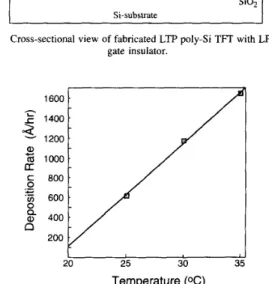
Fig. 2 shows a cross-sectional view of the fabricated poly-Si TIT. An under-layer of Si02 (500 nm thick) was thermally grown on a (100) silicon substrate. The polysilicon layer (100 nm thick) was prepared by the SPC method [ 5 ] . After the polysilicon layer was pattemed into islands, Si02 gate insulator (100 nm thick) was deposited at 40°C by the LPD method. Then gate polysilicon (350 nm thick) was deposited by LPCVD at 620°C and pattemed. P+ (5 x 10’’ cm-’, 40 KeV) self-aligned implanted source and drain regions were formed by thermal annealing for 24 hours at 600°C. After the interlayer of insulator was formed, the contact holes were opened, and an aluminum layer (500 nm thick) was evaporated and pattemed. Finally, hydrogenation was performed in a plasma reactor at 300°C for 60 min.
SiO,
~~~ ~ ~
Si-substrate
Fig. 2. Cross-sectional view of fabricated LTP poly-Si TIT with LPD Si02 gate insulator. 1 6 0 0 , 1400 h
-9
1200 a, ti 1000 U:6
8000”
.-
.-
c v) 600 0 a 400 200 L I Temperature (OC) Si02 film. 20 25 30 35Fig. 3. Dependence of deposition rate on deposition temperature for LPD
TABLE I LPD-Si02 CVD-SiO? ~~~~~~~~~ FTIR S i - 0 - S i Peak 1092.5 cm-1 1070 cm-l Refractive Index 1.43 1.45 P e t c h Rate 24 N s e c 2 5 N s e c Leakage Current Density 2 . 2 x 10-12 9.0 x 10⁻¹²
(at 5V) N c m 2 N c m 2
Dielectric Breakdown Field 7 MV/cm 5.8 MV/cm Dielectric Constant (1MHz) 3.5 4 . 3
111. RESULTS AND DISCUSSION A . Charucteristics of LPD S i 0 2 Film
The dependence of LPD Si02 deposition rate on deposition temperature is shown in Fig. 3, which indicates that the Si02 deposition rate is enhanced with the increase in deposition temperature.
The characteristics of LPD Si02 film are summarized in Table I, which also compares LPD Si02 and CVD Si02 [18]. For the LPD Si02 film, the refractive index is about 1.42 N 1.44, which is lower than the 1.462 of thermal Si02 but nearly the same as the value for CVD SiOz. The lower refractive index may be due to a porous structure [19]. This is consistent with the results for the P-etch rate. The P-etch rate of LPD Si02 is about 20 A/s. This value is larger than that for non-porous oxide (2
-
8 A/s) [19]. The dependence1.43 X a, 1.42
-
a,3
1.41 .- c c2
1.40 1.39 2 1 6 200 400 600 800 1000 Deposition Rate (hhr)Fig. 4. Dependence ofP-etch rate and refractive index on deposition rate for LPD Si02 film.
51-0-5,
4000 3000 2000 1000
Wavenumber (cm-1 )
Fig. 5. Fl'IR spectra of LPD Si02 and thermal SO;?. of refractive index and P-etch rate on LPD Si02 deposition rate is shown in Fig. 4. The refractive index increases but the P-etch rate decreases with a decrease in the deposition rate. This is because the film deposited at lower deposition rate has a denser (less porous) structure, which leads to a larger refractive index and a lower P-etch rate. Thus to control the film quality, it is necessary to select an optimal deposition condition with a low deposition rate.
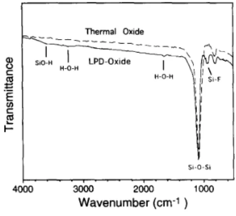
Typical FTIR spectra of LPD Si02 film are shown in Fig. 5. The absorption bands around 1090 cm-I and 810 cm-' are due to Si-0-Si stretching and bending vibration, respectively. These absorption bands are similar to those of thermal oxide, indicating that LPD oxide is amorphous in structure [19]. Another main absorption band around 930 cm-' found in the LPD Si02 spectra may be attributed to Si-F stretching vibration. The fluorine (F) contained in the Si-F bond must be incorporated from the H2SiF6 solution. At the same time, we find that only a few absorption bands related to water appear in the LPD Si02 spectrum. (O-H stretching due to H20 is shown in the absorption bands around 3300 cm-' and 1640 cm-l, while O-H stretching due to SiO-H is shown in the band around 3650 cm-I.) These bands reveal that LPD Si02 film contains only little water. Because this characteristic is very important for the electrical and structural stability of the film, we conclude that the LPD Si02 film is of good quality.
'::"f
80::b
,:Oxide4
4
0
0.0 2.0 4.0 6.0 8.0 10.0 12.0 1
Sputter Time (min) Fig. 6. AES depth profile of LPD S i 0 2 film.
I75
0
Electric Field (MV/cm)
Characteristics of current density versus electric field for LPD S i 0 2 MOS capacitors.
Fig. 7.
The AES depth profiles of LPD Si02 films are shown in Fig. 6. Only silicon (Si) and oxygen (0) atoms are detected in these films. The ratio of Si/O determined by AES is about 1/2 on the surface of the LPD Si02 films. However, the ratio of SUO is larger than 1/2 in the interior of the films. We conclude that LPD oxide films are Si-rich films. The Si- rich composition near the Si/SiO* interface thus influences the electrical characteristics of LPD Si02 films, as described below.
Fig. 7 is a typical current-voltage ( I - V ) curve of MOS capacitors with LPD Si02 film as dielectric. The leakage current density is about 3 nA/cm2 at an electric-field of 4 MV/cm, and the maximum breakdown electric-field (EBD) is about 7
-
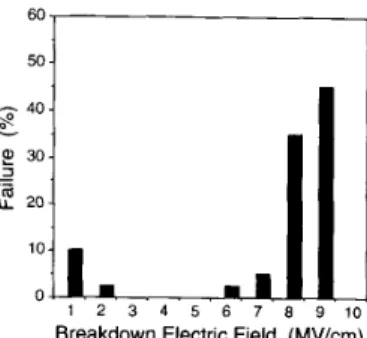
8 MV/cm. The leakage current densities of LPD Si02 film are slightly high. This may be due to the Si-rich composition of LPD Si02 film. The conduction mechanisms of LPD-oxide are similar to those reported for silicon-rich CVD Si02 [20]. That is, the current conduction in the Si-rich LPD Si02 film is likely to be due to direct tunneling from one Si-island to an adjacent one, and the characteristic hump in the I-V curve at high field probably results from Poole-Frenkel type conduction. The distribution of breakdown electric field( E B D ) is shown in Fig. 8; the maximum EBD of the LPD Si02 film is 8
-
9 MV/cm.Fig. 9 shows the C-V curves of MOS capacitors with LPD Si02 film as dielectric. The C-V curves reveal the presence of many positive charges, slow states, and fast states in the LPD Si02 film, which are related to oxygen vacancies. In addition, injection type hysteresis is observed in the inversion region.
176
-
4 0 - $-d
2 0 - E 30- 3 - . .- 501=.
. . . = . . - Breakdown Electric Field (MV/cm)Fig. 8. Distribution of breakdown electric field (EBu) for LPD Si02 MOS capacitors.
IEEE TRANSACTIONS ON ELECTRON DEVICES, VOL. 41, NO. 2, FEBRUARY 1994
-7 -6 -5 -4 -3 -2 -1 0 1 2 3
Voltage Bias (V)
Fig. 9. Typical capacitance versus voltage characteristics for MOS capacitors with LPD Si02 as dielectric.
Energy Level (eV)
Fig. 10. A typical distribution of interface trap density for MOS capacitors with LPD Si02 as dielectric.
It may result from fast trapping centers near the middle-gap correlated with the Si-rich structure. The Terman method [ 171 was used to calculate a typical distribution of interface-trap density (Dit), and the result is shown in Fig. 10. It appears one order of magnitude larger than the 1 x lolo cmP2 eV-l of thermal Si02 in the mid-gap, which makes it comparable to the value for CVD Si02.
The experimental results on the electrical characteristics of I-V and C-V are summarized in Table I. From the table, we can conclude that LPD Si02 film exhibits satisfactory electrical integrity.
lo-lllp
-20 -15 -10 -5 0 5 10 15 20 8
VGS (v)
5
Fig. 1 1. Typical drain current versus gate bias Characteristics for LTP poly-Si TFT’s with LPD Si02 gate insulator.
I
hydrogenation (3 hours)\
io- 5 10-1 1 -20 -15 -10 -5 0 5 10 15 20 25 VGS (v)Fig. 12. Comparison of drain current versus gate bias characteristics between as-fabricated and hydrogenated poly-Si TFT’s with LPD Si02 gate insulator.
B . Performance of LTP Poly-Si TFT’s
Fig. 11 shows the drain current versus gate bias (ID-VG) characteristics for W / L = 200 pm/lO pm poly-Si TFT’s with LPD Si02 gate insulator under constant drain voltage of 5 V and 10 V. Threshold voltage was determined from the extrapolated curve of the
6
- VG characteristics in the saturated region (VD = 10 V). Field-effect mobility was calculated from the maximum transconductance in the linear region (VD = 0.1 V). For these LTP poly-Si TFT’s, an on-off current ratio of 4.95 x IO6 at VD = 5V, field effect mobilityof 25.5 cm2/V.s at VD = 0.1 V, threshold voltage of 6.9 V, and subthreshold swing of 1.28 V/decade were obtained.
It is well known that carrier trapping, barrier formation, and dopant segregation in the network of grain boundaries and other defects in the Si/SiO:! interface can cause gross deviation in electronic properties from those of crystalline silicon. Hence to improve device performance, it is essential to reduce trap densities effectively. It has been shown that hydrogen plasma treatment can effectively reduce trap state density and improve device characteristics [21], [22]. A comparison of the I D - VG characteristics of as-fabricated and hydrogenated poly-Si TFT’s with LPD Si02 gate insulator is shown in Fig. 12. The characteristic parameters of poly-Si TFT’s obtained before and after hydrogenation are summarized in Table 11. The data in
YEH er al.: MECHANISMS OF LOW-TEMPERATURE PROCESSED POLYSILICON 177 TABLE I1
~~ ~ _ _ _ _ _ _ _ _ _ ~
As-fabricated Hydrogenation
(3 hours)
Field Effect Mobility 17.9 25.5
( c m W . sec)
Threshold Voltage (V) 12.9 6.91
Subthreshold Swing 2.11
(Vldec)
1.28
Trap State Density (cm-2) 7.25 x 4.2 x 1012
the table reveal that the field effect mobility has been improved from 17.9 cm2/V.s to 25.5 cm2/V.s, and the threshold voltage has been improved from 12.9 V to 6.9 V. Although the three- hour hydrogenation treatment markedly improves the electrical characteristics of poly-Si TFT’s, the hydrogenation time must far exceed three hours to greatly improve the performance of poly-Si TFT’s [23].
C. Off-State Current ( I L ) of LTP Poly-Si TFT’s
When negative gate bias (VGS) is applied, a considerable OFF-state current (I,) will be found. This current results from two basic mechanisms: 1) Resistive current, which arises when the applied VGS is not negatively large enough to form a p- layer in the channel region. In this case I L can be assumed to be an ohmic current flowing through the polysilicon bulk layer. This situation usually occurs when VGS is smaller than flat band voltage (VFB) but larger than the negative value of the threshold voltage (-Vth). 2) Junction leakage current, which arises when VGS is more negative than
-I&.
In that case, holes are induced to form a p-type channel region, and subsequently a reverse-biased p-n junction is formed between drain and channel. The junction leakage current is caused by electron-hole pairs generated via grain boundary traps in the depletion region.There are also three other, related mechanisms through which a trapped hole at an energy level Et can be generated to the valence band: (a) Pure thermal emission or thermal generation, which is due to thermal excitation of trapped holes in the valence band. (b) Pure field emission or tunneling, which is due to field ionization of trapped hole tunneling through the potential barrier into the valence band. (c) Thermionic field emission or Frenkel-Poole emission, which is due to field- enhanced thermal excitation of trapped holes in the valence band. The applied field causes the barrier to become low and thin enough that either thermal emission or thermal excitation to virtual states prior to tunneling can easily occur.
The pure field emission current has the strongest depen- dence on the applied field but is essentially independent of temperature, so it dominates at low temperature and high field conditions. The pure thermal emission current is proportional to the intrinsic carrier concentration ( n , ) of silicon, and n, is proportional to e x p [ - E , / 2 k ~ T ] (where E , is the energy gap of silicon). For this reason, the activation energy of the pure thermal emission current should be approximately equal
1 0 3 , 1 10-4 3 1 0 - 5 E 10-6 3 10-7 0
.r
10-8 2 n 10-9 v L Z T V Iw
Region I1-
10-10 10-1 1 Region I -30 -20 -10 0 10 20 30 Gate Voltage (V)Fig. 13. Dependence of OFF-state current on gate bias with drain bias as a parameter for LTP poly-Si TFT’s with LPD Si02 gate insulator.
WiL a: 100 p d l 0 pm b: 100 pn/20 pm c: 100 p d 3 0 pm IO- 3 10-4 .- f 10-8 - -10 0 10 20 30 Gate Voltage (V)
Fig. 14. Dependence of OFF-state current on gate bias at bb = 5 V for
poly-Si TIT’S with channel length as a parameter.
to E , / 2 . In addition, the pure thermal generation current is nearly independent of V&. On the other hand, both field emission and Frenkel-Poole emission current increase with V&. The difference between them is that the increase of the field emission current with ~ V G S
I
tends to approach a saturation value, while the Frenkel-Poole emission current does not [ 101. Furthermore, the activation energy of the latter is larger than that of the former.Fig. 13 shows the typical dependence of I L on VGS and
VDS for samples with W / L = 200 pm/20 pm, respectively. In order to distinguish the mechanism of the OFF-state current, the leakage current can be divided into three parts: 1) a low gate bias region I (at the region around -10 V
<
VGS<
0 V), 2) an almost flat region 11, in which I L does not change with a decrease in VGS, and 3 ) a gate-bias dependent region 111 at high drain bias. Although I L increases with negative VGS both in region I and region 111, the difference can be distinguished by the relationship between I L and V& with channel length (L) as a parameter (Fig. 14). I L in region I1 and region 111 is independent of L , while I L in region I decreases as L increases. The dependence of I L on 1/L, as shown in Fig. 15, indeed indicates that I L in region I varies linearly with 1/L. From the above description, it is obvious that I L in region I is a resistive current and I L in region I1 and region178 300- w = 1 5 0 p v D S = 5 v
-
VGS = - 4 v-
VGS'. 3 v 0.00 0.02 0.04 0.06 0.08 0.10 0.12 l/Channel Length (pm)-lFig. 15. Dependence of OFF-state current on the reverse of channel length at
Io
= 5 V for poly-Si TlT's with J4? = 150 pm.IEEE TRANSACTIONS ON ELECTRON DEVICES, VOL. 41, NO. 2, FEBRUARY 1994
W K 0.3 0 c
F
0.2 c 0 0.0-
-40 -20 0 20 40 Gate Voltage (V)Fig. 16. Dependence of activation energy on gate bias with drain bias at S
V and 10 V for poly-Si TIT'S with LPD Si02 gate insulator.
To further clarify the mechanism of I L in region I1 and
111, the temperature dependence was studied. The activation energies were calculated from an Arrhenius plot by means of leakage currents obtained at 25", 50", 75", IOO", and 125' C. The dependence of activation energy on VGS with VDS at 5 V and 10 V is shown in Fig. 16. The activation energies in region
11 are close to the
E,/2
of silicon and almost independent of V,. In contrast, an increase of negative VGS causes a decrease of activation energy in region 111. These results lead to the conclusion that I L is attributable to pure thermal generation in region I1 and to Frenkel-Poole emission in region 111. The width of region I1 is dependent on VDS. As VDS increases, the width of region 11 decreases. For devices at VDS = 5 V, I L is almost independent of VGS up to VGS = -30 V, and it vanishes when VDS = 10 V.Furthermore, according to [ 1 I], the Frenkel-Poole mecha- nism gives a current IFE of the form
where (3) (4) 1 0 - 8 - W/L = 50 y d l 0 pm h
9
s?
0 1 0 - 9 - c c L 3 a, m c8
10-10, . , . , . , . , . , . 500 600 700 800 900 1000 1' (Electric Field)l/2(V/cm)l/2 30Fig. 17. Measured log I L versus ( E ~ E ; ) ' / ' at \b = 10 V on a semilog scale for poly-Si TIT'S with W/L = SO pm/lO pm.
IO is the generation current at zero electric field, and EPK is the peak electric field given by
where E S ~ O ~ is the permittivity of silicon dioxide and
to,
is the thickness of silicon dioxide.Fig. 17 plots log I L versus ( E p ~ ) l / ~ at room temperature for our sample. A straight line fits the data reasonably well in the high electric field region. This also proves that I L in region 111 is dominated by Frenkel-Poole emission.
Although the above results and discussion are all in terms of n-channel poly-Si TFT's, similar results were obtained for p-channel poly-Si TFT's. In other words, the basic conduction mechanisms of OFF-state current in p-channel poly-Si TFT's also include resistive current, thermal generation current, and Frenkel-Poole emission current. However, the weight of each mechanism is different for n-channel and p-channel TFT's.
IV. CONCLUSION
Polysilicon thin film transistors using liquid phase depo- sition silicon dioxide (SiO2) as gate insulator were realized by low-temperature processes (< 620°C). The LPD Si02 method has been shown to be an economical approach that supplies a good dielectric layer. LTP poly-Si TFT's with W / L = 200 pm/lO pm have an on-off current ratio of 4.95 x IO6 at V, = 5 V, a field effect mobility of 25.5 cm2/V-s at V, = 0.1 V, a threshold voltage of 6.9 V, and a subthreshold swing of 1.28 VJdecade at V, = 0.1 V. Effective passivation of defects by plasma hydrogenation can improve the characteristics of these devices. The behavior of off-state current in LTP poly-Si TFT's has also been clarified. The conduction mechanisms of off-state currents can be divided into two parts, one attributable to a resistive current in the low gate bias region, the other to a junction leakage current in the high gate bias region. The junction leakage currents observed in our samples were due to two basic mechanisms, pure
YEH er al.: MECHANISMS OF LOW-TEMPERATURE PROCESSED POLYSILICON I79 thermal generation and Frenkel-Poole emission. Clarification
of leakage current mechanisms should enable us to find fundamental principles by which to reduce the off-state current.
REFERENCES
[ l ] J. Ohwada, “Driving condition for low temperature poly-Si LCD,” SID
Dig., 1986, p. 55.
[2] Y. Oana, “A 240 x 360 element active matrix LCD with integrated gate-bus drivers using poly-Si TFTs,” SID Dig., 1984, p. 312. [3] S. Morozumi, K. Oguchi, T. Misawa, R. Araki, and H. Ohshima. “4.25-
in. and 1.51-in. B/W and full-color LCD video displays addressed by poly-Si TFTs,” SID Dig., 1984, p. 316.
[4] J. Ohwada, “Peripheral drive circuits for poly-Si TFT LCD,” in E-rrended
Ahstr. 1987 (19th) Con5 Solid Stare Devices and Marerials, p. 55. [5] M. K. Hatalis and D. W. Greve, “High-performance thin-film transistors
in low-temperature crystallized LPCVD amorphous silicon films,” lEEE
Electron Device Left., vol. 8, p. 361, 1987.
[6] H. Ohshima and S. Morozumi, ‘‘Future trends for TIT integrated circuits on glass substrates,” in IEDM Tech Dig., p. 157, 1989.
[7] A. Mimura, T. Suzuki, N. Konishi, T. Suzuki, and K. Miyata, “Low- temperature polysilicon T I T with two-layer gate insulator using photo- CVD and APCVD SiOz,” IEEE Electron Device Lett., vol. 9, p. 290, 1988.
[8] C. F. Yeh, S. S. Lin, C. L. Chen, and Y. C. Yang, “Novel Technique for Si02 formed by Liquid-Phase Deposition for Low-Temperature Processed Polysilicon TlT,” IEEE Electron Device Left., vol. 14, p. 403, 1993.
[9] A. Chiang, I-W. Wu, M. Hack, A. G. Lewis, T. Y. Huang, and C-C. Tsai, “Polysilicon thin film transistor material and device technologies.” in Extended Abstr. 1991 Cont. Solid Stare Devices and Materials, p. 586. [lo] J. G. Fossum, A. Ortiz-Conde, H. Shichijo, and S . K. Banerjee. “Anomalous leakage current in LPCVD polysilicon MOSFET’s,” /EL%
Trans. Electron Dev., vol. ED-32, p. 1878, Sept. 1985.
[ l l ] S. K. Madan and D. A. Antoniadis, “Leakage current mechanisms in Hydrogen-passivated fine-grain polycrystalline silicon on insulator
MOSFET’s,”IEEE Trans. Electron Dei.., vol. ED-33, p. 15 18. Oct. 1986. [12] I . W. Wu, A. G. Lewis, T. Y. Huang, W. B. Jackson. and A . Chi- ang, “Mechanism and device-to-device variation of leakage current in polysilicon thin film transistors,” in 1EDM Tec.h Dig., p. 867, 1990. [13] P. Migliorato and D. B. Meakin, “Material properties and characteristics
of polysilicon transistors for large area electronics.” Applied Surfuce
Sci., vol. 30, p. 353, 1987
[ 141 S. D. Brotherton, J. R. Ayres, and N. D. Young, “Characterization of low temperature poly-Si thin film transistors,” So/id-.Sraru Elecrrori.. vol. 34.
no. 7, p. 671, 1991.
[15] M. Yazaki, S. Takenaka, and H. Ohshima, “Conduction mechanism of leakage current observed in metal-oxide-semiconductor transistors and poly-Si thin-film transistors,” Japan. J Appl. Phys.. vol. 31. p. 206. 1992.
[I61 K. Ono, T. Aoyama, N. Konishi, and K. Miyata. “Analysis of curreiit- voltage characteristics of low-temperature-processed polysilicon thin- film transistors,” IEEE Trans. Electron Dei,., vol. 9, p. 792. Apr. 1992. [I71 E. H. Nicollian and J. R. Brews, MOS (Metal O.Yide S e m i c ~ m l i ~ t o r J
Physics and Technology.
[I81 T. Homma, T. Katoh, Y. Yamada, I. Shimizu. and Y. Mardo. “A new interlayer formation technology for completely planarized multilevel interconnection by using LPD,” in Proc,. 1990 Symp. VLSI T c ~ h r i o l . . [I91 W. A. Pliskin, “Comparison of propertie, of dielectric tilms depovted
by various methods,” J . Vac. Sc.i. Techno/., vol. 14, p. 1064. 1977.
1201 D. J. DiMaria and D. W. Dong, “High current injection into S i 0 2 fi-om Si rich Si02 films and experimental applications,” ./. A p p l . Pliys.. LOI. 51, p. 2772, 1980.
1211 A . Mimura, N. Konishi, K. Ono. J. 1. Ohwada, Y. Hosokaua. Y. A. Ono, T. Suzaki, K. Miyata, and H. Kawakami. “High perfonnance low- temperature poly-Si ri-channel TITS for LCD.” lEEE Truns. Elrc.ri-ori
&%,ices, vol. 36, p. 351, 1989.
[22] T. I. Kamins and P. J. Marcoux, “Hydrogenation of transistors fabncated in polysilicon-silicon films,” IEEE Elecwori De1,ic.e Lett.. vol. EDL- I . p. 159, 1980.
[23] I. W. Wu, T. Y. Huang. W. B. Jackson. A. G. L e u h and A. Chiang. “Passivation kinetics of two types of defect\ in polysilicon T€T by plasma hydrogenation,” 1EEE E/rc,r!-ori D r i . i w Lerr.. vol. 12. p. 18 I,
1991.
New York: Wiley. p. 325. 1982.
pp. 3 4 .
Ching-Fa Yeh was born in Hsinchu, Taiwan, on September 20, 1948. He received the B. S. degree from National Oceanic University, Keelung, Tai- wan, ROC, in 1971, the M. S . and Ph.D. degrees from the University of Tokyo, Tokyo, Japan, in 1979 and 1982, respectively, all in electrical engineering. From 1982 to 1988, he was with the Fuji Xe- rox’s Electronic Technology Laboratories, Ebina, Japan, where his work concemed the research and development of semiconductor process technologies and devices, particularly on dry process technology and contact amorphous-Si Image sensor, and high-voltage MOSFET. He is now an Associate Professor at the Department of Electronics Engineering & Institute of Electronics, National Chiao-Tung University, Hsinchu, Taiwan. His research interests include thin-film transistor, power devices, silicon-wafer directly bonding technologies, and low-temperature processed materials and devices.
Dr. Yeh is a member of Japanese Journal Applied Physics Society, and he also as an oversea member of program committee of the international Conference on Solid State Devices and Materials.
Shyue-Shyh Lin was horn in Nantou, Taiwan, on November IO, 1967. He received the B.S. and M.S. degrees in electronics engineering from National Chiao-Tung University, Hsinchu, Taiwan, ROC, in 1990 and 1992, respectively. Currently, he is work- ing towards the Ph.D. degree in electronics engi- neering at National Chiao-Tung University.
His current research interest is in the research and development of liquid-phase deposition silicon diox- ide film and its application on the semiconductor devices.
Tzung-Zu Yang was bom in Pingtung, Taiwan, on July 1 1 . 1969. He received the B.S. and M.S. degrees in electronics engineering from National Chiao-Tung University in 1991 and 1993, respec- tively.
Currently, he is working with the Electronic Re- search and Service organization, Industrial Tech- nology Research Institute, Hsinchu, Taiwan, ROC, where he is engaged in the research of field emission display.
Chun-Lin Chen was bom in Tainan, Taiwan, on February 13. 1965. He received the B. S. degree in chemistry from Tam-Kang University, Taipei, Tai- wan, ROC, in 1988 and the M.S. degree in applied chemistry from National Chiao-Tung University in 1991. Currently. he is working towards the Ph.D. degree in electronics engineering at National Chiao- Tung University.
His current research interest IS in the research and development of liquid-phase deposition silicon diox- ide film and its application on the semiconductor devices
Yu-Chi Yang was horn in Maioli, Taiwan, on Jan- uary 21, 1968. He received the B.S. and M.S. degrees in electrophysics from National Chiao-Tung University in 1990 and 1992, respectively. Cur- rently, he is serving in the Chinese Army as a Second Lieutenant.